

 Manufacturers
VIA TECHNOLOGIES Eden ESP

Description
VIA Eden ESP Embedded System Platform Processor
Part Number
Eden ESP
Price
Request Quote
Manufacturer
VIA TECHNOLOGIES
Lead Time
Request Quote
Category
Processors
Features
- 64-KB Level 2 victim cache
- A proprietary Enhanced Ball Grid Array (EBGA) package that shares with Socket 370 processors features such as bus protocol and electrical interface
- AMD-compatible 3DNow! Instructions (Model 7)
- Branch Target Address Cache with 1k entries each identifying 2 branches (Model 9)
- Bus speeds up to 133 MHz
- Compact and economical EBGA packaging with excellent thermal dissipation characteristics
- Extremely low power dissipation for fanless operation
- MMX-compatible instructions for enhanced media performance
- Seamlessly software compatible with the thousands of available x86 software applications
- SSE-compatible instructions (Model 9)
- Two large (64-KB each, 4-way) on-chip Level 1 caches (2-way in Model 9 Stepping 8 and higher)
- Two large TLBs (128 entries each, 8-way) with two page directory caches
- Unique and sophisticated branch prediction mechanisms
- Very small die 52 mm2 in TSMC 0.13µ for Model 9 (47 mm2 for Stepping 8 and higher)
- Very small die 52 mm2 in TSMC 0.15µ for Model 7
Datasheet

Extracted Text
TM VIA Eden Embedded System Platform Processor Datasheet Revision 1.79 October 11, 2004 VIA TECHNOLOGIES, INC. VIA Eden ESP Processor Datasheet October 11, 2004 This is Version 1.79 of the VIA Eden ESP Processor Datasheet. © 2002-2004 VIA Technologies, Inc All Rights Reserved. VIA reserves the right to make changes in its products without notice in order to improve design or performance characteristics. This publication neither states nor implies any representations or warranties of any kind, including but not limited to any implied warranty of merchantability or fitness for a particular purpose. No license, express or implied, to any intellectual property rights is granted by this document. VIA makes no representations or warranties with respect to the accuracy or completeness of the contents of this publication or the information contained herein, and reserves the right to make changes at any time, without notice. VIA disclaims responsibility for any consequences resulting from the use of the information included herein. Cyrix, VIA C3, and VIA Eden ESP are trademarks of VIA Technologies, Inc. CentaurHauls is a trademark of Centaur Technology Corporation. AMD, AMD K6, and Athlon are trademarks of Advanced Micro Devices, Inc. Microsoft and Windows are registered trademarks of Microsoft Corporation. Intel, Pentium, Celeron, and MMX are registered trademarks of Intel Corporation. Other product names used in this publication are for identification purposes only and may be trademarks of their respective companies. LIFE SUPPORT POLICY VIA processor products are not authorized for use as components in life support or other medical devices or systems (hereinafter life support devices) unless a specific written agreement pertaining to such intended use is executed between the manufacturer and an officer of VIA. 1. Life support devices are devices which (a) are intended for surgical implant into the body or (b) support or sustain life and whose failure to perform, when properly used in accordance with instructions for use provided in the labeling, can be reasonably expected to result in a significant injury to the user. 2. This policy covers any component of a life support device or system whose failure to perform can cause the failure of the life support device or system, or to affect its safety or effectiveness. October 11, 2004 VIA Eden ESP Processor Datasheet Revision History Document Release Date Revision Initials 1.21 9/16/02 Added EBGA mechanical specification diagram EY 1.22 9/19/02 Modified V voltage in normal operating condition (Table 5-8) EY TT 1.3 10/31/02 Modified EBGA mechanical specification diagram from EY EBGA368 / 376 to EBGA 368 1.4 11/25/02 Corrected miscellaneous document inconsistencies EY 1.5 3/11/03 Removed “Preliminary Information” from document EY Modified EBGA ball diagram 1.51 3/14/03 VIH2.5 – Input High Voltage changed from 2.0V to 1.55V EY 1.52 5/23/03 Added ESP 3000 and 7000 info into table 5-12 EY Updated top marking specification 1.6 5/28/03 Fixed miscellaneous document inconsistencies and errors EY 1.61 6/10/03 Added ESP 3000/7000 info into table 5-12 ~ 5-15 EY 1.62 8/26/03 Updated table 5-7 EY 1.63 11/14/03 Added information on Model 9 processors EY 1.64 11/18/03 Updated table 5-3 EY 1.65 3/2/04 Updated table 5-8 JW 1.66 3/3/04 Updated figures 6-3, 6-4, 6-5 JW 1.67 3/25/04 Changed ball pitch spec on page 6-6 JW 1.68 4/12/04 Updated table 5-8 JW 1.69 5/10/04 Updated figure 6-2 JW 1.70 6/3/04 Added 200 MHz FSB processor information JW 1.71 6/14/04 Updated table 5-8 JW 1.72 6/18/04 Added timing diagrams JW 1.73 7/13/04 Updated top markings JW 1.74 7/21/04 Updated section 1-3, figure 6-5 and table 5-8 JW 1.75 7/30/04 Updated POWERGOOD information in figure 5-5, 5-6 and table JW 4-3 Added figure 6-2, 6-4 1.76 8/19/04 Updated figures 6-5, 6-6, table 5-8 and section 7-1 JW 1.77 9/8/04 Updated top marking diagrams JW 1.78 9/21/04 Removed 376 ball figures JW o 1.79 10/11/04 Updated figure 6-5: added 100 C information Revision History i VIA Eden ESP Processor Datasheet October 11, 2004 Updated table 5-8 Updated section 7-1, paragraph 1 ii October 11, 2004 VIA Eden ESP Processor Datasheet Table of Contents INTRODUCTION .........................................................................................................................................................1-1 ARCHITECTURE..........................................................................................................................................................2-1 2.2.1 general architecture & features..............................................................................................................2-3 2.2.2 instruction fetch .......................................................................................................................................2-6 2.2.3 instruction decode....................................................................................................................................2-7 2.2.4 branch prediction ....................................................................................................................................2-8 2.2.5 integer unit...............................................................................................................................................2-9 2.2.6 d-cache & datapath ...............................................................................................................................2-10 2.2.7 l2 cache .................................................................................................................................................2-10 2.2.8 fp unit.....................................................................................................................................................2-11 2.2.9 mmx unit ................................................................................................................................................2-11 2.2.10 3dnow! unit (Model 7).......................................................................................................................2-12 2.2.11 SSE unit (Model 9)...........................................................................................................................2-12 2.2.12 bus unit ..............................................................................................................................................2-12 2.2.13 power management............................................................................................................................2-12 PROGRAMMING INTERFACE..................................................................................................................................3-1 3.3.1 general.....................................................................................................................................................3-4 3.3.2 standard cpuid instruction functions .......................................................................................................3-4 3.3.3 extended cpuid instruction functions .......................................................................................................3-7 3.3.4 centaur extended cpuid instruction functions ........................................................................................3-10 3.3.5 processor identification .........................................................................................................................3-11 3.3.6 edx value after reset...............................................................................................................................3-11 3.3.7 control register 4 (cr4) ..........................................................................................................................3-12 3.3.8 Machine-Specific Registers....................................................................................................................3-12 HARDWARE INTERFACE .........................................................................................................................................4-1 4.1.1 differences................................................................................................................................................4-1 4.1.2 clarifications............................................................................................................................................4-2 4.1.3 omissions .................................................................................................................................................4-5 4.4.1 bist .........................................................................................................................................................4-11 4.4.2 jtag.........................................................................................................................................................4-11 4.4.3 debug port..............................................................................................................................................4-11 ELECTRICAL SPECIFICATIONS .............................................................................................................................5-1 5.2.1 recommended operating conditions.......................................................................................................5-11 5.2.2 maximum ratings ...................................................................................................................................5-13 5.2.3 dc characteristics...................................................................................................................................5-14 5.2.4 power dissipation...................................................................................................................................5-15 MECHANICAL SPECIFICATIONS............................................................................................................................6-1 Table of Contents iii VIA Eden ESP Processor Datasheet October 11, 2004 THERMAL SPECIFICATIONS................................................................................................................................... 7-1 MACHINE SPECIFIC REGISTERS.......................................................................................................................... A-1 A.1 GENERAL............................................................................................................................................................... A-1 A.2 CATEGORY 1 MSRS................................................................................................................................................ A-4 A.3 CATEGORY 2 MSRS................................................................................................................................................ A-8 iv Table of Contents October 11, 2004 VIA Eden ESP Processor Datasheet List of Figures FIGURE 2-1. THE VIA EDEN ESP PROCESSOR PIPELINE STRUCTURE...............................................................................2-5 FIGURE 4-1. POWER MANAGEMENT STATE DIAGRAM....................................................................................................4-10 FIGURE 5-1. BCLK GENERIC CLOCK TIMING WAVEFORM ..............................................................................................5-5 FIGURE 5-2. VALID DELAY TIMINGS................................................................................................................................5-5 FIGURE 5-3. SETUP AND HOLD TIMINGS...........................................................................................................................5-6 FIGURE 5-4. COLD/WARM RESET AND CONFIGURATION TIMINGS ...................................................................................5-6 FIGURE 5-5. POWER-ON SEQUENCE AND RESET TIMINGS.................................................................................................5-7 FIGURE 5-6. POWER DOWN SEQUENCING AND TIMINGS (VCC LEADING) .......................................................................5-8 FIGURE 5-7. POWER DOWN SEQUENCING AND TIMINGS (VTT LEADING)........................................................................5-9 FIGURE 5-8. STOP GRANT /SLEEP TIMING (BCLK STOPPING METHOD) ........................................................................5-10 FIGURE 5-9. STOP GRANT/SLEEP TIMING (SLP# ASSERTION METHOD).........................................................................5-10 FIGURE 6-1. VIA EDEN ESP PROCESSOR EBGA BALL DIAGRAM (BOTTOM VIEW)........................................................6-2 FIGURE 6-2. MECHANICAL SPECIFICATION – 368 EBGA PACKAGE ................................................................................6-6 FIGURE 6-3. PROCESSOR TOP MARKING - ESP 4000/5000 ..............................................................................................6-7 FIGURE 6-4. PROCESSOR TOP MARKING - ESP 3000/6000 ..............................................................................................6-8 FIGURE 6-5. PROCESSOR TOP MARKING - ESP 6000/7000/8000/10K .............................................................................6-9 List of Figures v VIA Eden ESP Processor Datasheet October 11, 2004 List of Tables TABLE 3-1. CPUID RETURN VALUES (EAX = 0)...........................................................................................3-4 TABLE 3-2. CPUID EAX RETURN VALUES (EAX = 1)..................................................................................3-4 TABLE 3-3. CPUID EDX RETURN VALUES (EAX = 1)..................................................................................3-5 TABLE 3-4. EXTENDED CPUID FUNCTIONS ...................................................................................................3-7 TABLE 3-5. L1 CACHE & TLB CONFIGURATION ENCODING..........................................................................3-8 TABLE 3-6. L2 CACHE CONFIGURATION ENCODING ......................................................................................3-9 TABLE 3-7. CR4 BITS....................................................................................................................................3-12 TABLE 4-1. BSEL FREQUENCY MAPPING.......................................................................................................4-2 TABLE 4-2. CORE VOLTAGE SETTINGS...........................................................................................................4-3 TABLE 4-3. BALL DESCRIPTIONS ....................................................................................................................4-6 TABLE 4-4. CLOCK RATIO...............................................................................................................................4-8 1 TABLE 5-1. SYSTEM BUS CLOCK AC SPECIFICATIONS (133 MHZ) ..............................................................5-1 1 TABLE 5-2. SYSTEM BUS CLOCK AC SPECIFICATIONS (100 MHZ) ..............................................................5-2 1,8 TABLE 5-3. BUS SIGNAL GROUPS AC SPECIFICATIONS ...............................................................................5-2 1, 2 TABLE 5-4. CMOS AND OPEN-DRAIN SIGNAL GROUPS AC SPECIFICATIONS .........................................5-3 TABLE 5-5. RESET CONFIGURATION AC SPECIFICATIONS AND POWER ON/POWER DOWN TIMINGS............5-3 1 TABLE 5-6. APIC BUS SIGNAL AC SPECIFICATIONS .....................................................................................5-4 1, 3, 4 TABLE 5-7. STOPGRANT/DEEP SLEEP AC SPECIFICATIONS .....................................................................5-4 TABLE 5-8. RECOMMENDED OPERATING CONDITIONS.................................................................................5-11 TABLE 5-9. V STATIC AND TRANSIENT TOLERANCE.................................................................................5-13 CC TABLE 5-10. MAXIMUM RATINGS.................................................................................................................5-13 TABLE 5-11. DC CHARACTERISTICS.............................................................................................................5-14 TABLE 5-12. CMOS DC CHARACTERISTICS.................................................................................................5-14 ABLE 5-13. NORMAL MODE V POWER CONSUMPTION ...........................................................................5-15 T CC TABLE 5-14. QUICKSTART V POWER CONSUMPTION ...............................................................................5-15 CC TABLE 5-15. SLEEP V POWER CONSUMPTION...........................................................................................5-16 CC TABLE 5-16. DEEP SLEEP V POWER CONSUMPTION .................................................................................5-16 CC TABLE 5-17. VTT-I/O POWER CONSUMPTION..............................................................................................5-16 TABLE 6-1. EBGA BALL CROSS REFERENCE .................................................................................................6-3 TABLE 7-1. EBGA θ AND θ .......................................................................................................................7-3 JC JA TABLE A-1. CATEGORY 1 MSRS ...................................................................................................................A-2 TABLE A-2. CATEGORY 2 MSRS ...................................................................................................................A-3 TABLE A-3. FCR BIT ASSIGNMENTS .............................................................................................................A-9 vi List of Tables October 11, 2004 VIA Eden ESP Processor Datasheet SECTION INTRODUCTION The VIA Eden Embedded System Platform Processor (VIA Eden ESP for short) is based upon a unique internal architecture and is manufactured using advanced 0.15µ / 0.13µ CMOS technology. The VIA Eden ESP architecture and companion chips provide a highly compatible, high-performance, low-cost, and low-power solution for the embedded, min-notebook, embedded, and Internet Appliance markets. The VIA Eden ESP is available in several operating frequencies. When considered individually, the compatibility, function, performance, cost, and power dissipation of the VIA Eden ESP family are all very competitive. Furthermore, the value added from the advanced EBGA packaging includes remarkable compactness, cost efficiency and excellent thermal characteristics. The VIA Eden ESP represents a breakthrough combination for enabling high-value, high-performance, low-power, fanless x86-based solutions. When considered as a whole, the VIA Eden ESP family offers a peerless level of value. 1.1 DATASHEET OUTLINE The intent of this datasheet is to make it easy for a direct user—a board designer, a system designer, or a BIOS developer—to use the VIA Eden ESP processor. The companion chipset is documented separately. Section 1 of the datasheet summarizes the key features of the VIA Eden ESP processor. Section 2 provides a detailed description of the internal architecture of the VIA Eden ESP processor. Section 3 specifies the primary programming interface. Section 4 does the same for the bus interface. Sections 5, 6, and 7 specify the classical datasheet topics of AC timings, ballouts, and mechanical specifications. Appendix A documents the VIA Eden ESP processor machine specific registers (MSRs). Section 1 Introduction 1-1 VIA Eden ESP Processor Datasheet October 11, 2004 1.2 BASIC FEATURES The VIA Eden ESP processor family currently consists of two basic models with several different MHz versions. Due to their low power dissipation, either model is ideally suited for both desktop and mobile applications. All versions share the following common features: � Extremely low power dissipation for fanless operation � A proprietary Enhanced Ball Grid Array (EBGA) package that shares with Socket 370 processors features such as bus protocol and electrical interface � Seamlessly software compatible with the thousands of available x86 software applications � MMX-compatible instructions for enhanced media performance � AMD-compatible 3DNow! Instructions (Model 7) � SSE-compatible instructions (Model 9) � Two large (64-KB each, 4-way) on-chip Level 1 caches (2-way in Model 9 Stepping 8 and higher) � 64-KB Level 2 victim cache � Two large TLBs (128 entries each, 8-way) with two page directory caches � Unique and sophisticated branch prediction mechanisms � Branch Target Address Cache with 1k entries each identifying 2 branches (Model 9) � Bus speeds up to 133 MHz 2 � Very small die 52 mm in TSMC 0.15µ for Model 7 2 2 � Very small die 52 mm in TSMC 0.13µ for Model 9 (47 mm for Stepping 8 and higher) � Compact and economical EBGA packaging with excellent thermal dissipation characteristics 1-2 Introduction Section 1 October 11, 2004 VIA Eden ESP Processor Datasheet 1.3 PROCESSOR VERSIONS Typically, there are five specification parameters that characterize different versions of a processor family: package, voltage, maximum case temperature, external bus speed, and internal MHz. The VIA Eden ESP processor is differentiated from the VIA C3 family by its extreme low power consumption, high performance, and low-profile Enhance Ball Grid Array packaging. The EBGA package is not only compact and economical, but delivers excellent thermal properties for truly Cool Processing. The internal operating frequency of a particular VIA Eden ESP processor chip is defined by two parameters: the specified external bus speed and the internal bus-clock multiplier. VIA Eden ESP chips come in two bus-speed versions: either 100MHz bus or 133 MHz bus. (Either version can also operate at 66MHz bus speeds.) Bus frequency select balls (BSEL 0 and BSEL 1) identify the appropriate bus speed (100 MHz or 133 MHz). The bus-clock multiplier is hardwired into initial VIA Eden ESP processors. For these, the ratio of the 1 internal processor clock speed to the externally supplied bus clock is frozen . Several different clock- multiplier versions are currently offered. Future VIA Eden ESP processors will not have the bus multiplier locked. They will carry the “S” designation. In these chips, the clock ratio is set using the external bus ratio balls, BR[4:0]. More information on these topics is included in Sections 4, 5, and 6 of this datasheet � The VIA Eden ESP processor is initially available in a variety of models: • VIA Eden ESP 3000 (4.5 x 66-MHz bus) 1.05V • VIA Eden ESP 4000 (4.0 x 100-MHz bus) 1.05V • VIA Eden ESP 5000 (4.0 x 133-MHz bus) 1.20V • VIA Eden ESP 6000 (4.5 x 133-MHz bus) 1.20V • VIA Eden ESP 6000 (5.0 x 133-MHz bus) 1.05V • VIA Eden ESP 7000 (5.5 x 133-MHz bus) 1.05V • VIA Eden ESP 8000 (6.0 x 133-MHz bus) 1.05V • VIA Eden ESP 10000 (7.5 x 133-MHz bus) 1.05V • VIA Eden ESP 10000 (5.0 x 200-MHz bus) 1.05V � Future versions of the VIA Eden ESP processor may provide other models with other speed grades and bus speed combinations. � Future versions of the VIA Eden ESP processor may have different voltages 1 Actually, it is semi-frozen. A VIA-unique machine specific register allows programming to temporarily change the hard-wired multiplier. This capability, documented in Appendix A, is intended for special BIOS situations and test and debug usage. Section 1 Introduction 1-3 VIA Eden ESP Processor Datasheet October 11, 2004 1.4 COMPETITIVE COMPARISONS Section 2 of this datasheet contains considerable detail about the unique internal design of the VIA Eden ESP processor. Such an internal architecture comparison, however, does not directly address the most important considerations of users: compatibility, availability, price, MHz, application performance, and power dissipation. For that reason, we do not provide a detailed architecture comparison with other processors in this datasheet. Following instead is the high-level summary of an internal-architecture comparison: � The VIA Eden ESP processor has better cache and TLB capabilities. These are critical to system performance for modern PC operating systems and applications. � The VIA Eden ESP has a generally simpler internal architecture. However, the VIA Eden ESP implements many advanced features critical to performance (such as sophisticated branch prediction) and is highly tuned for good application performance, especially on “integer” or office applications. � The VIA Eden ESP has a much smaller die size. � The VIA Eden ESP has much lower power dissipation at the same operating frequency than its competitors. � No competitive processor matches the VIA Eden ESP in terms of combined low-power, modest thermal demands, performance, flexible packaging and attractive pricing. 1-4 Introduction Section 1 October 11, 2004 VIA Eden ESP Processor Datasheet 1.5 COMPATIBILITY The VIA Eden ESP processor shares much with conventionally packaged x86 siblings. Knowledgeable board designers can leverage their existing designs with the VIA Eden ESP. In most cases, however, special BIOS is needed. Currently, BIOS support for the VIA Eden ESP is available from Award, AMI, Phoenix and Insyde. The Model 7 VIA Eden ESP processor requires external termination of bus signals. The Model 9 VIA Eden ESP processor does not require external termination of bus signals. Physical and bus compatibility is covered in more detail in Section 4 of this datasheet. The Model 7 VIA Eden ESP processor supports 3DNow! and MMX instructions. The Model 9 VIA Eden ESP processor supports SSE and MMX instructions. The VIA Eden ESP processor does NOT support multiple processors. These functions are defined as optional by, and are identified to software via, the CPUID instruction. The VIA Eden ESP processor carefully follows the protocol for defining the availability of these optional features. Both the additional and omitted optional features are covered in more detail in Section 3 of this datasheet. To verify compatibility of the VIA Eden ESP with real PC applications and hardware, VIA has performed extensive testing of hundreds of PC boards and peripherals, thousands of software applications, and all known operating systems. Indicative of this high compatibility, the VIA Eden ESP has obtained both Windows 98 and Windows NT certification. Section 1 Introduction 1-5 VIA Eden ESP Processor Datasheet October 11, 2004 This page is intentionally left blank. 1-6 Introduction Section 1 October 11, 2004 VIA Eden ESP Processor Datasheet SECTION ARCHITECTURE 2.1 INTRODUCTION The VIA Eden ESP processor architecture can be either “Samuel 2” for Model 7 or “Nehemiah” for Model 9. It is different from any other x86 processor architecture. This unique processor design provides a significantly smaller die size using less power than any other x86 CPU. The VIA Eden ESP processor features cores that lower power, improve performance (MHz and CPI) and further reduces die size and power. (The major differences between the VIA Eden ESP 4000/5000 processor and the VIA Eden ESP 6000 are highlighted in the descriptions below.) The VIA Eden ESP processor architecture is based on, and directly exploits, basic “facts” about the current x86 market, applications, and bus environment. While seemingly straightforward, these concepts are not exploited in other processor architectures. The major concepts that shape the VIA Eden ESP architecture are: Section 2 Architecture 2-1 VIA Eden ESP Processor Datasheet October 11, 2004 � Only a few instructions dominate x86 instruction execution time. On typical applications, over 90% of instruction execution time is due to a handful of basic x86 instructions. Most x86 instructions have no significant impact on performance. The VIA Eden ESP processor design optimizes performance of the most important x86 instructions while minimizing the hardware provided for the little-used x86 functions (infrequently used x86 instructions are primarily implemented in microcode). The resulting instruction execution speed of highly used instructions is as good or better than comparable processors. For example, the VIA Eden ESP processor executes x86 load-ALU-store instructions in only one clock as compared to several clocks on other processors. The execution time of little-used instructions is impacted to reduce die size, but this has no effect on real application performance. � Improving clock frequency has higher leverage than improving CPI. The result of advanced computer design approaches over the last few years has been that the improvements in cycles-per- instruction (CPI) often impact MHz improvements, and certainly impact die size. Our belief is that the best way to improve total performance and keep a small low-power die is to improve MHz. Thus, the VIA Eden ESP family architecture provides improved performance by optimizing MHz via a 12-stage (16-stage for Model 9) pipeline while maintaining a good CPI. Complex CPI-driven features such as out-of-order instruction execution are not implemented because they (1) impact MHz, (2) require a lot of die area and power, and (3) have little impact on real performance since… (the next point) � Memory performance is the limiting CPI performance factor. In modern PCs, the processor bus is slow compared to the internal clock frequency. Thus, off-chip memory-accesses dominate processor CPI as opposed to internal instruction execution performance. The VIA Eden ESP processor addresses this phenomenon by providing many specific features designed to reduce bus activity: large primary caches, large TLBs, aggressive prefetching, an efficient level-2 cache (new to the VIA Eden ESP 4000/5000 and 6000), and so forth. � Different market segments have different workload characteristics. The hardware, operating systems, and applications used in fanless PC’s, internet appliances, small form factor PC’s have different technical characteristics than those in the high-end, workstation, or server market. The VIA Eden ESP family exploits these differences by implementing very specific design tradeoffs, providing high performance with low cost in the target environments. These optimizations are based on extensive analysis of actual behavior of target-market hardware and software. � Small is beautiful. VIA Eden ESP processors are highly optimized for small die size. In addition to the obvious cost benefits, this small size reduces power consumption and improves reliability. 2-2 Architecture Section 2 October 11, 2004 VIA Eden ESP Processor Datasheet 2.2 COMPONENT SUMMARY 2.2.1 GENERAL ARCHITECTURE & FEATURES Figure 2-1 illustrates the basic 12-stage (integer) pipeline (16-stage for Model 9) structure of the VIA Eden ESP family. At a high level, there are four major functional groups: I-fetch, decode and translate, execution, and data cache. The I-fetch components deliver x86 instruction bytes from the large I-cache or the external bus. Large buffers allow fetching to proceed asynchronously to other operations. The decode and translate components convert x86 instruction bytes into internal execution forms. Branches are also identified, predicted, and the targets prefetched. Large buffers allow decoding and translating to proceed asynchronously to other operations. The execution components issue, execute, and retire internal instructions. The data cache components manage the efficient loading and storing of execution data to and from the caches, bus, and internal components. At one level the VIA Eden ESP processor architecture seems simple: instructions are issued, executed, and retired in order, only one instruction can be issued per clock, and most data cache misses stall the pipeline. However, the design is actually highly optimized and highly tuned to achieve high performance in the targeted environment. Some of the significant features providing this performance are: � High internal clock frequency. The 12-stage (16-stage for Model 9) pipeline facilitates high MHz � Large on-chip caches and TLBs. The VIA Eden ESP implements large caches and TLBs that significantly reduce stalls due to bus traffic. These primary caches and TLBs are larger than those on any other x86 processor: • Two 64-KB primary (L1) caches with 4-way associativity (2-way in Model 9 Stepping 8 and higher) • A 4-way (16-way for Model 9) 64-KB unified level-2 (L2) cache • Two 128-entry TLBs with 8-way associativity • Two 8-entry page directory caches that effectively eliminate loads of page directory entries upon TLB misses • A four-entry (8 bytes each) store queue that also forwards store data to subsequent loads • A four-entry write buffer that also performs write combining � Extensive features to further minimize bus stalls. These include: • Full memory type range registers (MTRRs) • A non-stalling write-allocate implementation • Implementation of the “cache lock” feature • Non-blocking out-of-order retirement of pipeline stores • Implementation of x86 prefetch instruction (3DNow!) • Implicit speculative data prefetch into D-cache • Aggressive implicit instruction prefetch into I-cache • Highly asynchronous execution with extensive queuing to allow fetching, decoding and translating, executing, and data movement to proceed in parallel Section 2 Architecture 2-3 VIA Eden ESP Processor Datasheet October 11, 2004 � High-performance bus implementation. The VIA Eden ESP socket 370 compatible bus implementation includes the following performance enhancements: • No stalls on snoops • Up to 8 transactions can be initiated by the processor • Aggressive write pipelining • Smart bus allocation prioritization • 100MHz, 133MHz and 200MHz bus operation � Good performance for highly used instructions. Heavily used instructions—including complex functions such as protect-mode segment-register loads and string instructions—are executed fast. In particular, the pipeline is arranged to provide one-clock execution of the heavily used register– memory and memory–register forms of x86 instructions. Many instructions require fewer pipeline clocks than on comparable processors. 2-4 Architecture Section 2 October 11, 2004 VIA Eden ESP Processor Datasheet I I-Cache & I-TLB 128-ent 8-way I-Fetch B 64 KB 4-way 8-ent PDC V predecode Return stack decode buffer 3 BHTs Decode F Branch Decode Prediction 4-entry inst Q & Translate BTB Translate X Socket L2 cache Bus 4-entry inst Q ROM 370 Bus Unit 64 Kb 4-way Register File R address calculation A D-Cache & D-TLB D 128-ent 8-way 64 KB 4-way 8-ent PDC G Execute FP Integer ALU E Q Store-Branch S MMX/ FP 3D Unit Writeback W Unit Store Buffers Write Buffers Figure 2-1. The VIA Eden ESP Processor Pipeline Structure Section 2 Architecture 2-5 VIA Eden ESP Processor Datasheet October 11, 2004 2.2.2 INSTRUCTION FETCH The first three pipeline stages (I, B, V) deliver aligned instruction data from the I-cache or external bus into the instruction decode buffers. These stages are fully pipelined such that on each clock cycle a new instruction fetch address is fetched from the I-cache and either 16 bytes (I-cache) or 8-bytes (bus) of instruction data is delivered for decode. The primary I-cache contains 64 KB organized as four-way set associative with 32-byte lines. The associated large I-TLB contains 128 entries organized as 8-way set associative. In addition, the I-TLB includes an eight-entry page directory cache that significantly reduces the TLB miss penalty. The cache, TLB, and page directory cache all use a pseudo-LRU replacement algorithm. As opposed to many other contemporary x86 processors, the data in the I-cache is exactly what came from the bus; that is, there are no “hidden” predecode bits. This allows a large cache capacity in a small physical size. The instruction data is predecoded as it comes out of the cache; this predecode is overlapped with other required operations and, thus, effectively takes no time. The fetched instruction data is placed sequentially into multiple buffers. Starting with a branch, the first branch-target byte is left adjusted into the instruction decode buffer (the XIB). As instructions are decoded, they are removed from the XIB. Each clock, new incoming fetch data is concatenated with the remaining data in the XIB. Once the XIB is filled, fetching continues to fill three 16-byte buffers that feed the XIB. If an I-cache miss occurs during the filling of the fetch buffers, up to four 32-byte lines are speculatively prefetched from the external bus into the cache. These prefetches are pipelined on the bus for optimal bus efficiency. This aggressive prefetch algorithm exploits the large size and four-way structure of the I-cache, as well as the high-bandwidth bus implementation. 2-6 Architecture Section 2 October 11, 2004 VIA Eden ESP Processor Datasheet 2.2.3 INSTRUCTION DECODE Instruction bytes in the XIB are decoded and translated into the internal format by two pipeline stages (F, X). These units are fully pipelined such that, in general, an x86 instruction is decoded and translated every clock cycle. The F stage decodes and “formats” an x86 instruction (completely contained in the XIB) into an intermediate x86 format. This process requires only one clock cycle for every x86 instruction. However, instruction prefixes other than 0F require an additional cycle for each prefix. The internal-format instructions are placed into a five-deep FIFO queue: the FIQ. The FIQ facilitates the asynchronous fetch and “lookahead” capability of the formatter such that the extra cycles for prefixes rarely result in a bubble in the execution pipeline. The FIQ also allows for branch prediction to proceed even if the pipeline ahead of the branch is stalled. The X-stage “translates” an intermediate-form x86 instruction from the FIQ into the internal micro- instruction format. The output of the translator contains: (1) the internal micro-instruction stream to perform the x86 instruction function, (2) the immediate data fields from the x86 instruction, and (3) various x86 state information used to control execution (for example, operand size). The internal micro- instruction stream consists of micro-instructions directly generated by the translator plus, in some cases, an on-chip ROM address. The translator can generate up to three micro-instructions per clock plus a ROM address. Most x86 instructions except for repetitive string operations are translated in one clock. Executable micro-instructions can come from either the XIQ or the on-chip ROM. For performance- sensitive instructions, there is no delay due to access of micro-code from ROM. The microcode ROM capacity is larger than most x86 microcode ROMs to allow unimportant (relative to performance) functions to be performed in microcode (versus in hardware). The large size also allows the inclusion of extensive self-test microcode and extensive built-in debugging aids (for processor design debug). Instruction fetch, decode, and translation are made asynchronous from execution via a five-entry FIFO queue (the XIQ) between the translator and the execution unit. This queue allows the formatter and translator to “look-ahead” and continue translating x86 instructions even though the execution unit is stalled. Section 2 Architecture 2-7 VIA Eden ESP Processor Datasheet October 11, 2004 2.2.4 BRANCH PREDICTION The VIA Eden ESP processor implements a very unique and sophisticated, yet relatively small, branch prediction mechanism. Several different mechanisms predict all basic types of branches: jumps and calls using a displacement, returns, indirect jumps and calls, and “far” (inter-segment) branches (new to the VIA Ezra core). These types of jumps represent almost 25% of all instructions executed. The prediction starts when the branch is decoded in the F stage. If a branch is predicted taken, the target is fetched such that a four-clock “bubble” appears to occur. In practice however, this bubble averages less than two clocks due to the extensive instruction queuing below the F stage; the delay in fetching the predicted branch target is absorbed by execution of these queued instructions. There is also a special case: short forward branches that “hit” in the XIB require only one clock delay. For displacement-from branches, the target address is directly calculated. This direct calculation of the target address eliminates the need for a large branch-target buffer (a BTB or BTAC). The direct calculation always produces the correct address whereas a BTB often mispredicts the address, or fails to predict at all. Two different prediction algorithms are used to predict the direction of conditional branches. The underlying theory behind this approach is that, in practice, branches tend to fall into two categories. Most branches can be accurately predicted by a classic mechanism using a counter associated with the branch location. The associated VIA Eden ESP processor mechanism is a simple array of predictors 4K in the Samuel 2 core. However, about 20% of branches are hard to predict, because whether they branch or not depends on dynamic execution state. The VIA Eden ESP processor mechanism for predicting these pattern-based branches uses a 13-bit global branch history XOR’d with the branch instruction address to index a branch history table with 8K entries in the Nehemiah core versus 4K in the Samuel 2 core. This branch-history mechanism is called g-share in the technical literature. A third 4K-entry table selects which predictor (simple or history-based) to use for a particular branch based on the previous behavior of the branch. All three predictor tables actually use a one-bit “agree/disagree” predictor rather than the conventional two-bit counter. This unique approach uses a static predictor that considers the type of conditional branch and what type of instruction previously set the condition flag being tested. Rather than indicate taken or not, the one-bit entry in the predictor tables predicts whether the conditional branch direction agrees with the static prediction. The static predictor is accurate about 70% of the time, and the dynamic predictor is accurate about 95% of the time. In addition, x86 return instructions are predicted by a 16-entry return-address stack. This prediction is about 90% accurate. Finally, indirect jump and call instructions are predicted using a conventional 64-entry (4-way) in the Samuel 2 core. This small array predicts about 75% of indirect branches correctly. The BTB is also used to predict inter-segment (“far”) branches. 2-8 Architecture Section 2 October 11, 2004 VIA Eden ESP Processor Datasheet 2.2.5 INTEGER UNIT Internal micro-instructions are executed in a tightly coupled seven-stage (integer) pipeline that is similar in structure to a basic four-stage RISC pipeline with extra stages for memory loads and stores inserted. These extra stages allow instructions that perform a load and ALU operation, or a load, ALU, and store operation to execute in one clock. The micro-instructions and associated execution units are highly tuned for the x86 architecture. The micro-instructions closely resemble highly used x86 instructions. Examples of specialized hardware features supporting the x86 architecture are: hardware handling of the x86 condition codes, segment descriptor manipulation instructions, and hardware to automatically save the x86 floating-point environment. The integer execution stages are: � Decode stage (R): Micro-instructions are decoded, integer register files are accessed and resource dependencies are evaluated. � Addressing stage (A): Memory addresses are calculated and sent to the D-cache. The VIA Eden ESP processor is capable of calculating most x86 instruction address forms in one clock; a few forms containing two registers or a shifted index register require two clocks. Addresses can be automatically incremented or decremented for implementing stack and string operations. Some ALU operations are duplicated in this stage to reduce AGI (address generation interlock) stalls. For example, the sequence of adding to the stack pointer register followed by using it in a return does not cause an AGI. In general, register adds and moves are performed in the A-stage. � Cache Access stages (D, G): The D-cache and D-TLB are accessed and aligned load data returned at the end of the G-stage. The cache is fully pipelined such that a new load or store can be started and data returned each clock. � Execute stage (E): Integer ALU operations are performed. All basic ALU functions take one clock except multiply and divide. Load-ALU and Load-ALU-store instructions require only one clock (the data is loaded before the ALU stage). Results from the ALU can be forwarded to any instruction following the ALU instruction using a unique result-forwarding cache. Branch instructions are evaluated in this stage and, if incorrectly predicted, the corrected branch address is sent to the I-cache during the next clock. No additional action is required for correctly predicted branches. During this stage the floating-point, MMX, and 3DNow! execution units access their registers or consume the load data just delivered. These execution units “hang off” the end of the main execution unit so that load-ALU operations for these units can be pipelined in one clock. � Store stage (S): Integer store data is grabbed in this stage and placed in a store buffer. Positioning stores in this stage allows a one-clock load–ALU–store instruction. MMX and floating-point stores, however, are placed in the store buffer in a subsequent cycle due to their deep pipelines. � Write-back stage (W): The results of operations are committed to the register file. Section 2 Architecture 2-9 VIA Eden ESP Processor Datasheet October 11, 2004 2.2.6 D-CACHE & DATAPATH The D-cache contains 64 KB organized as four-way set associative with 32-byte lines. The associated large D-TLB contains 128 entries organized as 8-way set associative. In addition, the D-TLB includes an eight-entry page directory cache that significantly reduces the TLB miss penalty. The cache, TLB, and page directory cache all use a pseudo-LRU replacement algorithm. Associated with the D-cache are store and write buffers. All stores that pass the W-stage are placed in a four-entry store buffer (8 bytes each). Stores from the store buffer are drained to the D-cache or bus in actual program order, regardless of when the data appeared in the store buffers. Stores that miss the D- cache percolate to the write buffers where they wait for the bus. If the memory region is defined as write- combining, the stores can combine in the write buffers. 2.2.7 L2 CACHE The VIA Eden ESP processor contains an efficient level-2 cache. This L2 cache is exclusive (this approach is sometimes called a “victim” cache). This means that the contents of the L2 cache at any point in time are not contained in the two 64-KB L1 caches. As lines are displaced from the L1 caches (due to bringing in new lines from memory), the displaced lines are placed in the L2 cache. Thus, a future L1- cache miss on this displaced line can be satisfied by returning the line from the L2 cache instead of having to access the external memory. Thus, the total effective cache size on the VIA Eden ESP processor is 192 KB (two 64-KB L1 caches and the 64-KB L2). Processors, such as the Intel Celeron processor, that have an inclusive L2 cache have a total effective cache size equal to the L2 size (128 KB in the case of the current Intel Celeron processor). This is because the contents of the L1 caches are duplicated within an inclusive L2 cache. The L2 cache is also “unified;” that is, it contains lines displaced from both the L1 I-cache and the L1 D- cache. Thus the L2 cache provides a significant assist for the cases where an I-fetch hits in the L1 data cache, or a data reference hits in the L1 I-cache. To provide correct execution semantics, these cases require the hit line to be ejected from the L1 cache. The VIA Eden ESP processor L2 cache is 64 KB organized as four-way set associative with 32-byte lines and uses a pseudo-LRU replacement algorithm. 2-10 Architecture Section 2 October 11, 2004 VIA Eden ESP Processor Datasheet 2.2.8 FP UNIT In addition to the integer execution unit, the VIA Eden ESP processor has a separate 80-bit floating-point execution unit that can execute x86 floating-point instructions in parallel with integer instructions. Since the VIA Eden ESP processor is designed for mainstream applications that stress integer performance, floating-point throughput is not a priority. The FP unit is clocked at ½ the processor clock speed; that is, in an 800-MHz VIA Eden ESP, the FP-unit runs at 400 MHz. Floating-point instructions proceed through the integer R, A, D, and G stages. Thus, load-ALU x86 floating-point instructions do not require an extra clock for the load. Floating-point instructions are then passed from the integer pipeline to the FP-unit through an 8-instruction FIFO queue (new to the VIA Eden ESP). This queue, which runs at the processor clock speed, decouples the slower running FP unit from the integer pipeline so that the integer pipeline can continue to process instructions overlapped with up to eight FP instructions. Basic arithmetic floating-point instructions (add, multiply, divide, square root, compare, etc.) are represented by a single internal floating-point instruction. Certain little-used and complex floating point instructions (sin, tan, etc.), however, are implemented in microcode and are represented by a long stream of instructions coming from the ROM. These instructions “tie up” the integer instruction pipeline such that integer execution cannot proceed until they complete. One floating-point instruction can issue form the FP queue to the FP unit every two clocks. The FP pipeline is six-stages deep following the E stage. It is partially pipelined: a non-dependent add or multiply can start every two clocks. 2.2.9 MMX UNIT The VIA Eden ESP processor contains a separate execution unit for the MMX-compatible instructions. MMX instructions proceed through the integer R, A, D, and G stages. Thus, load-ALU x86 MMX instructions do not require an extra clock for the load. One MMX instruction can issue into the MMX unit every clock. The MMX multiplier is fully pipelined and can start one non-dependent MMX multiply[-add] instruction (which consists of up to four separate multiplies) every clock. Other MMX instructions execute in one clock. Multiplies followed by a dependent MMX instruction require two clocks. Architecturally, the MMX registers are the same as the floating-point registers. However, there are actually two different register files (one in the FP-unit and one in the MMX units) that are kept synchronized by hardware. Section 2 Architecture 2-11 VIA Eden ESP Processor Datasheet October 11, 2004 2.2.10 3DNOW! UNIT (MODEL 7) The VIA Eden ESP (Model 7) processor contains a separate execution unit for the 3DNow! instructions. These instructions are compatible with the AMD K6-II processor 3DNow! instructions and provide performance assists for graphics transformations via new SIMD single-precision floating-point capabilities. 3DNow! instructions proceed through the integer R, A, D, and G stages. Thus, load-ALU x86 3DNow! instructions do not require an extra clock for the load. One 3DNow! instruction can issue into the 3DNow! unit every clock The 3DNow! unit has two single-precision floating-point multipliers and two single-precision floating- point adders. Other functions such as conversions, reciprocal, and reciprocal square root are provided. The multiplier and adder are fully pipelined and can start any non-dependent 3DNow! instruction every clock. 2.2.11 SSE UNIT (MODEL 9) The VIA Eden ESP processor (Model 9) contains a separate execution unit for the SSE instructions. These instructions are compatible with the other x86 processors supporting SSE instructions and provide performance assists for graphics transformations via new SIMD single-precision floating-point capabilities. SSE instructions proceed through the integer R, A, J, D, G and H stages. Thus, load-ALU x86 SSE instructions do not require an extra clock for the load. One SSE instruction can issue into the SSE unit every clock. The SSE unit has two single-precision floating-point multipliers and two single-precision floating-point adders. Other functions such as conversions, reciprocal, and reciprocal square root are provided. The multiplier and adder are fully pipelined and can start any non-dependent SSE instruction every clock. 2.2.12 BUS UNIT The VIA Eden ESP bus unit provides an external bus interface, supporting bus speeds of 100 MHz and 133 MHz. The VIA Eden ESP processor bus implementation has no stalls on snoops, up to eight transactions can be generated (versus four), and stores are more heavily pipelined on the bus. 2.2.13 POWER MANAGEMENT Power management is not a component but rather a pervasive feature in all components. There are two major modes: powering down components based on bus signals such as stop clock and sleep, and dynamically powering off components during execution when they are not needed. The VIA Eden ESP processor implements the bus-controlled power management modes including: autoHALT power down state, stop grant state, sleep state, and deep sleep, or stop clock, state. While in normal running state, all major functional components are powered off when not in use. All caches, tags and TLBs are turned on and off on a clock-by-clock basis based on their usage. Other major components such as the MMX unit, the 3DNow! unit, the SSE unit, the FP unit, and the ROM are turned on and off as used. In addition, even in blocks that are powered up, internal buses and latches hold their values when not needed to reduce dynamic power consumption. 2-12 Architecture Section 2 October 11, 2004 VIA Eden ESP Processor Datasheet SECTION PROGRAMMING INTERFACE 3.1 GENERAL The VIA Eden ESP processor’s functions include: � All basic x86 instructions, registers, and functions � All floating-point (numeric processor) instructions, registers and functions � All basic operating modes: real mode, protect mode, virtual-8086 mode � System Management Interrupt (SMI) and the associated System Management Mode (SMM) � All interrupt and exception functions � All debug functions (including the new I/O breakpoint function) � All input/output functions � All tasking functions (TSS, task switch, etc.) � Processor initialization behavior � Page Global Enable feature The VIA Eden ESP processor, in addition to the MMX instructions, also includes 3DNow! (Model 7) and SSE (Model 9) instructions to boost the performance of 3D graphics. Section 3 Programming Interface 3-1 VIA Eden ESP Processor Datasheet October 11, 2004 However, there are some differences between the VIA Eden ESP and the Celeron processor. These differences fall into three groups: � Implementation-specific differences. Examples are cache and TLB testing features, and performance monitoring features that expose the internal implementation features. These types of functions are incompatible among all different x86 implementations. � Omitted functions. Some Intel Celeron processor functions are not provided on the VIA Eden ESP processor because they are not used or are not needed in the targeted PC systems. Examples are some specific bus functions such as functional redundancy checking and performance monitoring. These types of differences are similar to those among various versions of the processors. The CPUID instruction is used by system software to determine whether these features are supported. � Low-level behavioral differences. A few low-level VIA Eden ESP processor functions are different from Intel Celeron because the results are (1) documented in the documentation as undefined, and (2) known to be different for different x86 implementations. That is, compatibility with the Intel Celeron processor for these functions is clearly not needed for software compatibility (or they would not be different across different implementations). � EBGA package. The VIA Eden ESP processor is exclusively produced in an advanced, inexpensive, compact and thermally efficient EBGA package. This chapter summarizes the first three types of differences: additional functions, implementation-specific functions, and omitted functions. Appendix A contains more details on machine-specific functions. 3-2 Programming Interface Section 3 October 11, 2004 VIA Eden ESP Processor Datasheet 3.2 ADDITIONAL FUNCTIONS The VIA Eden ESP processor (Model 7) includes AMD-compatible 3DNow! instructions to boost the performance of 3D applications. These instructions are not defined in this datasheet but are defined in the appropriate AMD documentation. The VIA Eden ESP processor (Model 9) includes SSE instructions to boost the performance of 3D applications. The VIA Eden ESP processor (Model 9 Stepping 8 and higher) also includes the functions listed below. Virtual 8086 Mode Enhancements: VME VME has been added to VIA Eden ESP (Model 9) stepping ID 8 and above. The function is omitted in VIA Eden ESP (Model 9) stepping ID 7 and below. The CPUID feature flag bit 1 will indicate if Virtual Mode Enhancements are present. SYSENTER and SYSEXIT: SEP This function has been added to VIA Eden ESP (Model 9) stepping ID 8 and above. The function is omitted in VIA Eden ESP (Model 9) stepping ID 7 and below. The CPUID feature flag bit 11 will indicate if SYSENTER/SYSEXIT instructions are present. Page Attribute Table: PAT PAT function has been added to VIA Eden ESP (Model 9) stepping ID 8 and above. The function is omitted in VIA Eden ESP (Model 9) stepping ID 7 and below. The CPUID feature flag bit 16 will indicate if a Page Attribute Table is present. Section 3 Programming Interface 3-3 VIA Eden ESP Processor Datasheet October 11, 2004 3.3 MACHINE-SPECIFIC FUNCTIONS 3.3.1 GENERAL All x86 processor implementations provide a variety of machine-specific functions. Examples are cache and TLB testing features and performance monitoring features that expose the internal implementation features. This section describes the VIA Eden ESP processor machine-specific functions that are most likely used by software, and compares them to related processors where applicable. Appendix A describes the VIA Eden ESP machine-specific registers (MSRs). This section covers those features of Intel Pentium-compatible processors that are used to commonly identify and control processor features. All Pentium-compatible processors have the same mechanisms, but the bit-specific data values often differ. 3.3.2 STANDARD CPUID INSTRUCTION FUNCTIONS The CPUID instruction is available on all contemporary x86 processors. The CPUID instruction has two standard functions requested via the EAX register. The first function returns a vendor identification string in registers EBX, ECX, and EDX. The second CPUID function returns an assortment of bits in EAX and EDX that identify the chip version and describe the specific features available. The EAX:EBX:ECX:EDX return values of the CPUID instruction executed with EAX == 0 are: Table 3-1. CPUID Return Values (EAX = 0) REGISTER[BITS] – MEANING VIA EDEN ESP EAX 1 (highest EAX input value understood by CPUID) EBX:EDX:ECX “Centaur (vendor ID string) Hauls” The EAX return values of the CPUID instruction executed with EAX == 1 are: Table 3-2. CPUID EAX Return Values (EAX = 1) EAX BITS - MEANING VIA EDEN ESP 3:0 - Stepping ID Same as the return 7:4 - Model ID value in EDX after Reset (see next section) 11:8 - Family ID 13:12 – Type ID 3-4 Programming Interface Section 3 October 11, 2004 VIA Eden ESP Processor Datasheet The EDX return values of the CPUID instruction with EAX == 1 are: Table 3-3. CPUID EDX Return Values (EAX = 1) VIA EDEN VIA EDEN VIA EDEN EDX BITS – MEANING MODEL 9 MODEL 9 NOTES MODEL 7 (Stepping 0-7) (Stepping 8-15) 0 - FPU present 1 1 1 1 - Virtual Mode Extension 0 0 1 2 - Debugging Extensions 1 1 1 3 - Page Size Extensions (4MB) 0 1 1 4 - Time Stamp Counter (TSC) supported 1 1 1 5 - Model Specific Registers present 1 1 1 6 - Physical Address Extension 0 0 0 7 - Machine Check Exception 0/1 0 0 8 - CMPXCHG8B instruction 0/1 1 1 1 9 - APIC supported 0 0 1 2 10- Reserved 11- Fast System Call 0 0 1 12- Memory Range Registers 1 1 1 13 - PTE Global Bit supported 1/0 1/0 1/0 3 14- Machine Check Architecture supported 0 0 0 15- Conditional Move supported 0 1 1 16- Page Attribute Table 0 0 1 17- 36-bit Page Size Extension 0 0 0 18- Processor serial number 0 0 0 19:22 – Reserved 23 – MMX supported 1 1 1 24 – FXSR 0 1 1 25 – Streaming SIMD Extension supported 0 1 1 26:31 – Reserved Notes On CPUID Feature Flags: General: an “x/y” entry means that the default setting of this bit is x but the bit (and the underlying function) can be set to y using the FCR MSR. 1. The CMPXCHG8B instruction is provided and always enabled, however, it appears disabled in the corresponding CPUID function bit 0 to avoid a bug in an early version of Windows NT. However, this default can be changed via a bit in the FCR MSR. 2. APIC will be available in future steppings of Model 9 VIA Eden ESP processors. Section 3 Programming Interface 3-5 VIA Eden ESP Processor Datasheet October 11, 2004 3. The VIA Eden ESP processor’s support for Page Global Enable can be enabled or disabled by a bit in the FCR. The CPUID bit reports the current setting of this enable control. 3-6 Programming Interface Section 3 October 11, 2004 VIA Eden ESP Processor Datasheet 3.3.3 EXTENDED CPUID INSTRUCTION FUNCTIONS The VIA Eden ESP supports extended CPUID functions. These functions provide additional information about the VIA Eden ESP. Extended CPUID functions are requested by executing CPUID with EAX set to any value in the range 0x80000000 through 0x80000006. The following table summarizes the extended CPUID functions. Table 3-4. Extended CPUID Functions EAX TITLE OUTPUT 80000000 Largest Extended Function EAX=80000006 Input Value EBX,ECX,EDX=Reserved 80000001 Processor Signature and EAX=Processor Signature Feature Flags EBX,ECX=Reserved EDX=Extended Feature Flags 80000002 Processor Name String EAX,EBX,ECX,EDX 80000003 Processor Name String EAX,EBX,ECX,EDX 80000004 Processor Name String EAX,EBX,ECX,EDX 80000005 TLB and L1 Cache Information EAX = Reserved EBX = TLB Information ECX = L1 Data Cache Information EDX = L1 Instruction Cache Information 80000006 L2 Cache Information EAX, EBX, EDX = Reserved ECX = L2 Cache Information Largest Extended Function Input Value (EAX==0x80000000) Returns 0x80000006 in EAX, the largest extended function input value. Processor Signature and Feature Flags (EAX==0x80000001) For VIA Eden ESP (Model 9) processors, no information is returned when CPUID is executed with EAX==0x80000001. For VIA Eden ESP (Model 7) processors, the CPUID instruction returns processor version information in EAX, this value is identical to the value of EDX after RESET. Returns feature flags in EDX, this value is identical to the value in EDX after CPUID standard function 1, with the exception of bit 31: EDX[31]=0 3DNow! instructions not supported. EDX[31]=1 3DNow! instructions supported. Note that if FCR[20]=0 then 3DNow! instructions are not supported and EDX[31] will be 0. Section 3 Programming Interface 3-7 VIA Eden ESP Processor Datasheet October 11, 2004 Processor Name String (EAX==0x80000002–0x80000004) Returns the name of the processor, suitable for BIOS to display on the screen (ASCII). The string can be up to 48 characters in length. If the string is shorter, the rightmost characters are padded with zero. The leftmost characters go in EAX, then EBX, ECX, and EDX. The leftmost character goes in least significant byte (little endian). For example, the string “VIA Ezra” would be returned by extended function EAX=0x80000002 as follows: EAX = 0x20414956 EBX = 0x61727A45 ECX = 0x00000000 EDX = 0x00000000 Since the string is less than 17 bytes, the extended functions EAX=0x80000003 and EAX=0x80000004 return zero in EAX, EBX, ECX, and EDX. L1 Cache Information (EAX == 0x80000005) Returns information about the implementation of the TLBs and caches: Table 3-5. L1 Cache & TLB Configuration Encoding REGISTER DESCRIPTION VALUE EAX Reserved EBX TLB Information EBX[31:24] D-TLB associativity 8 EBX[23:16] D-TLB # entries 128 EBX[15: 8] I-TLB associativity 8 EBX[ 7: 0] I-TLB # entries 128 ECX L1 Data Cache Information ECX[31:24] Size (Kbytes) 64 ECX[23:16] Associativity 4/2 ECX[15: 8] Lines per Tag 1 ECX[ 7: 0] Line Size (bytes) 32 EDX L1 Instruction Cache Information EDX[31:24] Size (Kbytes) 64 EDX[23:16] Associativity 4/2 EDX[15: 8] Lines per Tag 1 EDX[ 7: 0] Line Size (bytes) 32 Notes On CPUID L1 Cache Associativity: For VIA Eden ESP (Model 9) processors, steppings 0 through 7 have a 4-way L1 Data and Instruction caches. Steppings 8 and higher have 2-way L1 Data and Instruction caches. Stepping 8 has an erratum that will inadvertently report 4-way L1 caches instead of the proper 2-way L1 caches. The erratum is fixed in future steppings. 3-8 Programming Interface Section 3 October 11, 2004 VIA Eden ESP Processor Datasheet L2 Cache Information (EAX == 0x80000006) Returns information about the implementation of the L2 cache: Table 3-6. L2 Cache Configuration Encoding REGISTER DESCRIPTION VALUE EAX, EBX, EDX Reserved ECX L2 Data Cache Information ECX[31:24] Size (Kbytes) 64 ECX[23:16] Associativity 4/16 ECX[15: 8] Lines per Tag 1 ECX[ 7: 0] Line Size (bytes) 32 Notes On CPUID L2 Cache Associativity: For VIA Eden ESP (Model 9) processors, L2 Data cache is 16 way. Section 3 Programming Interface 3-9 VIA Eden ESP Processor Datasheet October 11, 2004 3.3.4 CENTAUR EXTENDED CPUID INSTRUCTION FUNCTIONS The VIA Eden ESP processor (Model 9) supports special CPUID functions. These functions provide additional information about the VIA Eden ESP processor. Centaur CPUID functions are requested by executing CPUID with EAX set to 0xC0000000 or 0xC0000001. EAX INPUT TITLE OUTPUT Largest Centaur Extended Function Input 0xC0000000 EAX=0xC0000001 Value EDX=Centaur Extended Feature Flags 0xC0000001 Centaur Extended Feature Flags EAX,EBX,ECX=Reserved EDX BIT VALUE EDX[0]=0 Alternate Instruction Set (AIS) not supported 0 EDX[0]=1 Alternate Instruction Set (AIS) supported EDX[1]=0 AIS Disabled 1 EDX[1]=1 AIS Enabled EDX[2]=0 Random Number Generator (RNG) Present 2 EDX[2]=1 Random Number Generator (RNG) Not Present EDX[3]=0 RNG Disabled 3 EDX[3]=1 RNG Enabled EDX[4]=0 Longhaul MSR 0x110A not available 4 EDX[4]=1 Longhaul MSR 0x110A available EDX[5]=0 FEMMS instruction (opcode 0x0F0E) Not Present 5 EDX[5]=1 FEMMS instruction (opcode 0x0F0E) Present 31:6 Reserved 3-10 Programming Interface Section 3 October 11, 2004 VIA Eden ESP Processor Datasheet 3.3.5 PROCESSOR IDENTIFICATION The VIA Eden ESP processor provides several machine-specific features. These features are identified by the standard CPUID function EAX=1. Other machine-specific features are controlled by VIA Eden ESP processor MSRs. Some of these features are not backward-compatible with the predecessors in the IDT WinChip family. System software must not assume that all future processors in the VIA processor family will implement all of the same machine-specific features, or even that these features will be implemented in a backward- compatible manner. In order to determine if the processor supports particular machine-specific features, system software should follow the following procedure. Identify the processor as a member of the VIA processor family by checking for a Vendor Identification String of “CentaurHauls” using CPUID with EAX=0. Once this has been verified, system software must determine the processor version in order to properly configure the machine-specific registers. In general system software can determine the processor version by comparing the Family and Model Identification fields returned by the CPUID standard function EAX=1. If the processor version is not recognized then system software must not attempt to activate any machine- specific feature. 3.3.6 EDX VALUE AFTER RESET After reset the EDX register holds a component identification number as follows: 31:14 13:12 11:8 7:4 3:0 EDX Reserved Type ID Family ID Model ID Stepping ID 18 2 4 4 4 The specific values for the VIA Eden ESP 4000/5000/6000 are: PROCESSOR TYPE ID FAMILY ID MODEL ID STEPPING ID VIA Eden ESP 3000 0 6 7 Begins at 0 / 4000 / 5000 / 6000 The specific values for the VIA Eden ESP 7000/8000/10000 are: PROCESSOR TYPE ID FAMILY ID MODEL ID STEPPING ID VIA Eden ESP 7000 0 6 9 Begins at 0 / 8000 / 10000 Section 3 Programming Interface 3-11 VIA Eden ESP Processor Datasheet October 11, 2004 3.3.7 CONTROL REGISTER 4 (CR4) Control register 4 (CR4) controls some of the advanced features of the Celeron processor. The VIA Eden ESP provides a CR4 with the following specifics: Table 3-7. CR4 Bits CELERON CELERON CR4 BITS – MEANING VIA EDEN NOTES MODEL 6 MODEL 8 0: VME: Enables VME feature 0/1 0/1 0/1 1 1: PVI: Enables PVI feature 0/1 0/1 0/1 1 2: TSD: Makes RDTSC inst privileged 0/1 0/1 0/1 3: DE: Enables I/O breakpoints 0/1 0/1 0/1 4: PSE: Enables 4-MB pages 0/1 0/1 0/1 1 5: PAE: Enables address extensions r r r 6: MCE: Enables machine check exception 0/1 0/1 0/1 2 7: PGE: Enables global page feature 0/1 0/1 0/1 8: PCE: Enables RDPMC for all levels 0/1 0/1 0/1 9: OSFXSR: Enables FXSAVE//FXRSTOR Support 0/1 r 0/1 3 10: OSXMMEXCPT: O/S Unmasked Exception Support 0/1 r 0/1 3 31:11 – reserved r r r Notes On CR4 General: a “0/1” means that the default setting of this bit is 0 but the bit can be set to (1). A “0” means that the bit is always 0; it cannot be set. An “r” means that this bit is reserved. It appears as a 0 when read, and a GP exception is signaled if an attempt is made to write a 1 to this bit. 1. The VIA Eden ESP processors Model 7 and Model 9 Stepping 7 and below do not provide this “Appendix A” function and this CR4 bit cannot be set. However, no GP exception occurs if an attempt is made to set this bit. The VIA Eden ESP processor Model 9 steppings 8 and above do provide the function and the CR4 bit can be set. 2. The VIA Eden ESP processor Machine Check has different specifics than the Machine Check function of compatible processors. 3. The VIA Eden ESP processor (Model 7) do not provide this function and this CR4 bit cannot be set. This bit is a reserved bit on Model 7 processors. 3.3.8 MACHINE-SPECIFIC REGISTERS The VIA Eden ESP processor implements the concept of Machine Specific Registers (MSRs). RDMSR and WRMSR instructions are provided and the CPUID instruction identifies that the VIA Eden ESP processor supports MSRs. In general, the MSRs have no usefulness to application or operating system software and are not used. (This is to be expected since the MSRs are different on each processor.) Appendix A contains a detailed description of the VIA Eden ESP’s MSRs. 3-12 Programming Interface Section 3 October 11, 2004 VIA Eden ESP Processor Datasheet 3.4 OMITTED FUNCTIONS This section summarizes those functions that are not in the VIA Eden ESP processor. A bit in the CPUID feature flags indicates whether these feature are present or not. Physical Address Extensions: PAE This function is omitted since the target market for the VIA Eden ESP processor is small form factor PC’s, Internet appliances, and fanless PC’s. These systems do not use 2 MB paging or have greater than 4 GB of system memory. Page Size Extensions: PSE-36 This function is omitted since the target operating systems for the VIA Eden ESP processor do not require greater than 4 GB of system memory. Other Functions There are other functions that are not implemented in the VIA Eden ESP processor. These are identified accordingly in the CPUID feature flags and vary based on the model and stepping of the processor. Model specific registers pertaining to Machine Check, and Debug, Performance Monitoring, and Trace features are not supported. Section 3 Programming Interface 3-13 VIA Eden ESP Processor Datasheet October 11, 2004 This page is intentionally left blank. 3-14 Programming Interface Section 3 October 11, 2004 VIA Eden ESP Processor Datasheet SECTION HARDWARE INTERFACE 4.1 BUS INTERFACE The VIA Eden ESP bus interface is functionally similar to the Socket 370 interface. The majority of the balls within the bus interface are involved with the physical memory and I/O interface. The remaining balls are for power and ground, test and debug support, and various ancillary control functions. The balls and associated functions are listed and described in this section. 4.1.1 DIFFERENCES The areas where the VIA Eden ESP processor differs from compatible processors should not cause operational compatibility issues. These differences are: � Bus-to-core Ratio Control � Bus Frequency Control � Probe Mode / JTAG / TAP Port (see section test & debug) Bus-to-Core Frequency Ratio Control The VIA Eden ESP processor supports both fused and software control of the bus-to-core frequency ratio. At reset, the factory-set, fused ratio is used. This ratio can then be adjusted via software (PowerSaver 1.0) for VIA Eden ESP Model 7 processors. This adjustment lasts until the next reset. For VIA Eden ESP Model 9 processors, software can adjust the bus-to-core ratio using the VIA C3 Nehemiah processor’s LongHaul extensions. These are documented separately in the VIA C3 LongHaul Specification. This adjustment lasts until the next reset. Section 4 Hardware Interface 4-1 VIA Eden ESP Processor Datasheet October 11, 2004 Bus Frequency Selection The VIA Eden ESP processor supports automated bus frequency selection through the BSEL balls. The BSEL balls are used as a mechanism whereby the processor and the system board can negotiate to support high frequency bus frequencies. The standard BSEL decoding is shown in Table 4-1. While the VIA Eden ESP processor is designed to operate at bus frequencies of 66, 100, or 133 MHz, performance is improved by running at higher bus frequencies. Various speed bins preclude 133 MHz operation because the available bus-to-core ratios do not permit operation at the desired core MHz. Processors from these speed bins indicate this by shorting the BSEL[1] ball to ground internal to the package. For these processors the BSEL[0] ball is left floating. Processors from speed bins which permit 133 MHz bus operation indicate this by allowing both BSEL[1] and BSEL[0] to float. It is anticipated that motherboards will pull up both BSEL balls. The resulting BSEL-indicated bus frequency will then be either 100 MHz or 133 MHz according to speed bin. Bus operation at 66MHz is not desirable. Table 4-1. BSEL Frequency Mapping BSEL[1] BSEL[0] BUS FREQUENCY 0 0 66 MHz 0 1 100 MHz 1 0 Reserved 1 1 133 MHz 4.1.2 CLARIFICATIONS Power Supply Voltage The VIA Eden ESP automatically controls its core processor power supply voltage with the VID balls. The VID mapping for the VIA Eden ESP is in Table 4-2. This mapping corresponds to the VRM8.5 specification. 4-2 Hardware Interface Section 4 October 11, 2004 VIA Eden ESP Processor Datasheet Table 4-2. Core Voltage Settings VID4 VID3 VID2 VID1 VID0 VCORE 0 0 1 0 0 1.050V 1 0 1 0 0 1.075V 0 0 0 1 1 1.100V 1 0 0 1 1 1.125 0 0 0 1 0 1.150V 1 0 0 1 0 1.175V 0 0 0 0 1 1.200V 1 0 0 0 1 1.225V 0 0 0 0 0 1.250V 1 0 0 0 0 1.275V 0 1 1 1 1 1.300V 1 1 1 1 1 1.325V 0 1 1 1 0 1.350V 1 1 1 1 0 1.375V 0 1 1 0 1 1.400V 1 1 1 0 1 1.425V 0 1 1 0 0 1.450V 1 1 1 0 0 1.475V 0 1 0 1 1 1.500V 1 1 0 1 1 1.525V 0 1 0 1 0 1.550V 1 1 0 1 0 1.575V 0 1 0 0 1 1.600V 1 1 0 0 1 1.625V 0 1 0 0 0 1.650V 1 1 0 0 0 1.675V 0 0 1 1 1 1.700V 1 0 1 1 1 1.725V 0 0 1 1 0 1.750V 1 0 1 1 0 1.775V 0 0 1 0 1 1.800V 1 0 1 0 1 1.825V Section 4 Hardware Interface 4-3 VIA Eden ESP Processor Datasheet October 11, 2004 VCCCMOS The VIA Eden ESP renames VCC1.5 and VCCCMOS as VTT power pins. This signal is not used by the processor, but is intended to be used by the system as the power supply for CMOS level signals. VCCCMOS should not be expected to source more than 250mA. RESET# The VIA Eden ESP processor is reset by the assertion of the RESET# ball, T-3. Thermal Monitoring The VIA Eden ESP processor supports thermal monitoring via the THERMDN and THERMDP balls. Advanced Peripheral Interrupt Controller (APIC) The APIC is currently not supported by the VIA Eden ESP processor. Future steppings of the VIA Eden ESP (Model 9 Stepping 8 and higher) processor will support the APIC. The APIC balls (PICCLK, PICD0, and PICD1) are specified as reserved, but should be connected on the motherboard for compatibility with future processors. Driver Termination VIA Eden ESP (Model 7) processors require external termination. System boards must terminate signals to ensure correct operation. VIA Eden ESP (Model 9) processors support on-die termination and do NOT require external termination. RTTCTRL VIA Eden ESP (Model 7) processors do not connect to the RTTCTRL ball. VIA Eden ESP (Model 9) processors use the RTTCTRL ball to control integrated I/O pull-ups. For compatibility with all processors, the motherboard should be designed to use RTTCTRL. NCHCTRL VIA Eden ESP (Model 7) processors do not connect to the NCHCTRL ball. VIA Eden ESP (Model 9) processors use the NCHCTRL ball to control the output impedance. For compatibility with all processors, the motherboard should be designed to use NCHCTRL. 4-4 Hardware Interface Section 4 October 11, 2004 VIA Eden ESP Processor Datasheet 4.1.3 OMISSIONS Breakpoint and Performance Monitoring Signals The VIA Eden ESP processor internally supports instruction and data breakpoints. However, the VIA Eden ESP processor does not support the external indication of breakpoint matches. Similarly, the VIA Eden ESP processor contains performance monitoring hooks internally, but it does not support the indication of performance monitoring events. Error Checking The VIA Eden ESP processor does not support error checking. The BERR#, BINIT#, AERR#, AP#[1:0], DEP#[7:0], IERR#, RP#, and RSP# signals do not exist. Section 4 Hardware Interface 4-5 VIA Eden ESP Processor Datasheet October 11, 2004 4.2 BALL DESCRIPTION Table 4-3. Ball Descriptions Ball Name Description I/O Clock A[31:3]# The address Bus provides addresses for physical memory and external I/O devices. I/O BCLK During cache inquiry cycles, A31#-A3# are used as inputs to perform snoop cycles. A20M# A20 Mask causes the CPU to make (force to 0) the A20 address bit when driving the I (VTT) ASYNC external address bus or performing an internal cache access. A20M# is provided to emulate the 1 MByte address wrap-around that occurs on the 8086. Snoop addressing is not affected. ADS# Address Strobe begins a memory/I/O cycle and indicates the address bus (A31#-A3#) I/O BCLK and transaction request signals (REQ#) are valid. BCLK Bus Clock provides the fundamental timing for the VIA Eden ESP CPU. The frequency I (2.5V) - of the VIA Eden ESP CPU input clock determines the operating frequency of the CPU’s bus. External timing is defined referenced to the rising edge of CLK. BNR# Block Next Request signals a bus stall by a bus agent unable to accept new I/O BCLK transactions. BPRI# Priority Agent Bus Request arbitrates for ownership of the system bus. I BCLK BR[4:0] Hardware strapping options for setting the processors internal clock multiplier. Future I BCLK VIA Eden ESP processors do not have their clock multiplier set to a factory default value. Use jumpers or populate 0Ω resistors to select the rated multiplier. The BR[4:0] balls should be wired to VSS for a value of “0” or wired to OPEN for setting of “1.” See Table 4-4 for ratio values. BSEL[1:0] Bus Selection Bus provides system bus frequency data to the CPU. O (3.3V) BCLK BRB[1:0]# BRB0# drives the BREQ[0]# signal in the system to request access to the system bus. I/O None BRB1# drives the BREQ[1]# signal in the system to request access to the system bus. CFUSE0 VIA Eden ESP (Model 9 Stepping 9 and higher) CFUSE0 enables APIC when I None grounded, when CFUSE0 is allowed to float APIC is disabled D[63:0]# Data Bus signals are bi-directional signals which provide the data path between the VIA I/O BCLK Eden ESP CPU and external memory and I/O devices. The data bus must assert DRDY# to indicate valid data transfer. DBSY# Data Bus Busy is asserted by the data bus driver to indicate data bus is in use. I/O BCLK DEFER# Defer is asserted by target agent (e.g., north bridge) and indicates the transaction I BCLK cannot be guaranteed as an in-order completion. DRDY# Data Ready is asserted by data driver to indicate that a valid signal is on the data bus. I/O BCLK FERR# FPU Error Status indicates an unmasked floating-point error has occurred. FERR# is O (VTT) ASYNC asserted during execution of the FPU instruction that caused the error. FLUSH# Flush Internal Caches writing back all data in the modified state. I (VTT)) ASYNC HIT# Snoop Hit indicates that the current cache inquiry address has been found in the cache I/O BCLK (exclusive or shared states). 4-6 Hardware Interface Section 4 October 11, 2004 VIA Eden ESP Processor Datasheet Ball Name Description I/O Clock HITM# Snoop Hit Modified indicates that the current cache inquiry address has been found in I/O BCLK the cache and dirty data exists in the cache line (modified state). INIT# Initialization resets integer registers and does not affect internal cache or floating point I (VTT)) ASYNC registers. INTR / LINT0 Maskable Interrupt / APIC signal when enabled on Model 9 Stepping 8 and higher I (VTT)) ASYNC NMI / LINT1 Non-Maskable Interrupt / APIC signal when enabled on Model 9 Stepping 8 and higher I (VTT) ASYNC LOCK# Lock Status is used by the CPU to signal to the target that the operation is atomic. I/O BCLK NCHCTRL VIA Eden ESP (Model 9) processors use the NCHCTRL ball to control integrated I/O I ASYNC pull-ups. Connect this signal to VTT with a 14Ω resistor. PICCLK APIC clock for operation with the system I/O APIC, VIA Eden ESP (Model 9) I APIC processors only PICD[1:0] Bi-directional serial pins for communicating APIC messages to the system, VIA Eden I/0 APIC ESP (Model 9) processors only PWRGD Indicates that the processor’s VCC is stable. I (1.5V) ASYNC REQ[4:0]# Request Command is asserted by bus driver to define current transaction type. I/O BCLK RESET# Resets the processor and invalidates internal cache without writing back. I BCLK RTTCTRL VIA Eden ESP (Model 9) processors use the RTTCTRL ball to control the output I ASYNC impedance. Connect this signal to VSS with a 56Ω resistor if relying upon on-die termination. Connect this signal to VSS with a 110Ω resistor if relying upon board termination. RS[2:0]# Response Status signals the completion status of the current transaction when the I BCLK CPU is the response agent. SLP# Sleep, when asserted in the stop grant state, causes the CPU to enter the sleep state. I (VTT) ASYNC SMI# System Management (SMM) Interrupt forces the processor to save the CPU state to I (VTT) ASYNC the top of SMM memory and to begin execution of the SMI services routine at the beginning of the defined SMM memory space. An SMI is a high-priority interrupt than NMI. STPCLK# Stop Clock causes the CPU to enter the stop grant state. I (VTT) ASYNC TRDY# Target Ready indicates that the target is ready to receive a write or write-back transfer I BCLK from the CPU. VID[4:0] Voltage Identification Bus informs the regulatory system on the motherboard of the O (1.5V) ASYNC CPU Core voltage requirements. Section 4 Hardware Interface 4-7 VIA Eden ESP Processor Datasheet October 11, 2004 Table 4-4. Clock Ratio BR[4] BR[3] BR[2] BR[1] BR[0] Bus Ratio 0 0 0 0 0 9.0X 0 0 0 0 1 3.0X 0 0 0 1 0 4.0X 0 0 0 1 1 10.0X 0 0 1 0 0 5.5X 0 0 1 0 1 3.5X 0 0 1 1 0 4.5X 0 0 1 1 1 9.5X 0 1 0 0 0 5.0X 0 1 0 0 1 7.0X 0 1 0 1 0 8.0X 0 1 0 1 1 6.0X 0 1 1 0 0 12.0X 0 1 1 0 1 7.5X 0 1 1 1 0 8.5X 0 1 1 1 1 6.5X 1 0 0 0 0 Reserved 1 0 0 0 1 11.0X 1 0 0 1 0 12.0X 1 0 0 1 1 Reserved 1 0 1 0 0 13.5X 1 0 1 0 1 11.5X 1 0 1 1 0 12.5X 1 0 1 1 1 10.5X 1 1 0 0 0 13.0X 1 1 0 0 1 15.0X 1 1 0 1 0 16.0X 1 1 0 1 1 14.0X 1 1 1 0 0 Reserved 1 1 1 0 1 15.5X 1 1 1 1 0 Reserved 1 1 1 1 1 14.5X 4-8 Hardware Interface Section 4 October 11, 2004 VIA Eden ESP Processor Datasheet 4.3 POWER MANAGEMENT The VIA Eden ESP processor provides both static and dynamic power management. The VIA Eden ESP processor supports five power management states: NORMAL, QUICKSTART, SLEEP, DEEP SLEEP, and DEEPER SLEEP state. The DEEPER SLEEP state is available on VIA Eden ESP (Model 9) processors. The VIA Eden ESP processor uses dynamic power management techniques to reduce power consumption in the NORMAL state. In NORMAL state, the on-chip arrays, selected datapaths, and the associated control logic are powered down when not in use. Also, units that are in use attempt to minimize switching of inactive nodes. � NORMAL state is the normal operating state for the processor. � QUICKSTART state is the low power state where most of the processor clocks do not toggle. It is entered when the STPCLK# signal is asserted or when the processor executes the HALT instruction. Snoop cycles are supported in this state. � SLEEP state is the low power state where only the processor's PLL (phase lock loop) toggles. It is entered from QUICKSTART state when the processor samples the SLP# signal asserted. Snoop cycles that occur while in SLEEP state or during a transition into or out of SLEEP state will cause unpredictable behavior. � DEEP SLEEP state is a very low power state. It is entered when the BCLK signal is stopped while the processor in is the SLEEP state. Snoop cycles will be completely ignored in this state. � DEEPER SLEEP state is the lowest power state. It is entered when the processor core voltage is lowered while the processor is in the DEEP SLEEP state. Snoop cycles are completely ignored in this state. Section 4 Hardware Interface 4-9 VIA Eden ESP Processor Datasheet October 11, 2004 BCLK stopped STPCLK# or BCLK on HLT instruction and !SLP# Normal Quick Start halt break or !STPCLK# SLP# BCLK stopped snoop snoop !SLP# serviced occurs Sleep Deep Sleep BCLK on and SLP# Core Voltage Snoop Lowered Core Voltage Raised Deeper Sleep Figure 4-1. Power Management State Diagram 4-10 Hardware Interface Section 4 October 11, 2004 VIA Eden ESP Processor Datasheet 4.4 TEST & DEBUG 4.4.1 BIST A Built-in Self-Test (BIST) can be requested as part of the VIA Eden ESP reset sequence by holding INIT# asserted as RESET# is de-asserted. The VIA Eden ESP processor BIST performs the following general functions: � A hardware-implemented exhaustive test of (1) all internal microcode ROM, and (2) the X86 instruction decode, instruction generation, and entry point generation logic. � An extensive microcode test of all internal registers and datapaths. � An extensive microcode test of data and instruction caches, their tags, and associated TLBs. BIST requires about four million internal clocks. EAX Value After Reset The result of a BIST is indicated by a code in EAX. Normally EAX is zero after reset. If a BIST is requested as part of the Reset sequence, EAX contains the BIST results. A 0 in EAX after BIST Reset means that no failures were detected. Any value other than zero indicates an error has occurred during BIST. 4.4.2 JTAG The VIA Eden ESP processor has a JTAG scan interface that is used for test functions and the proprietary Debug Port. However, the VIA Eden ESP does not provide a fully compatible IEEE 1149.1 JTAG function. From a practical user viewpoint, JTAG does not exist and the associated balls (TCLK, and so forth) should not be used. 4.4.3 DEBUG PORT Certain processors have a proprietary Debug Port which uses the JTAG scan mechanism to control internal debug features (“probe mode”). These interfaces are not documented and are available (if at all) only under a non-disclosure agreement. The VIA Eden ESP processor does not have a debug interface. Section 4 Hardware Interface 4-11 VIA Eden ESP Processor Datasheet October 11, 2004 This page is intentionally left blank. 4-12 Hardware Interface Section 4 October 11, 2004 VIA Eden ESP Processor Datasheet SECTION ELECTRICAL SPECIFICATIONS 5.1 AC TIMING TABLES 1 Table 5-1. System Bus Clock AC Specifications (133 MHz) SYMBOL PARAMETER MIN MAX UNIT FIGURE NOTES System Bus Frequency 133 MHz T BCLK Period 7.5 7.65 ns Figure 5-1 (2) 1S T BCLK Period – Instantaneous Minimum 7.25 (2) 1Sabs T BCLK Period Stability +250 ps (2),(3),(4) 2S T BCLK High Time 1.4 ns Figure 5-1 at>2.0V 3S T BCLK Low Time 1.4 ns Figure 5-1 at<0.5V 4S T BCLK Rise Time 0.4 1.6 ns Figure 5-1 (5) 5S T BCLK Fall Time 0.4 1.6 ns Figure 5-1 (5) 6S Notes: 1. All AC timings for bus and CMOS signals are referenced to the BCLK rising edge at 1.25V. 2. Period, jitter, skew and offset measured at 1.25V. 3. Not 100% tested. Specified by design/characterization 4. Measured on the rising edge of adjacent BCLKs at 1.25V. The jitter present must be accounted for as a component of BCLK skew between devices. 5. Measured between 0.5V and 2.0V. Section 5 Electrical Specifications 5-1 VIA Eden ESP Processor Datasheet October 11, 2004 1 Table 5-2. System Bus Clock AC Specifications (100 MHz) SYMBOL PARAMETER MIN MAX UNIT FIGURE NOTES System Bus Frequency 100 MHz T BCLK Period 10 ns Figure 5-1 (2) 1S1 T BCLK Period – Instantaneous Minimum 9.75 ns (2) 1S1abs T BCLK Period Stability +250 ps (2), (3), (4) 2S1 T BCLK High Time 2.70 ns Figure 5-1 At>2.0V 3S1 T BCLK Fall Time 2.45 ns Figure 5-1 At<0.5V 4S1 T BCLK Rise Time 0.4 1.6 ns Figure 5-1 (5) 5S1 T BCLK Fall Time 0.4 1.6 ns Figure 5-1 (5) 6S1 Notes: 1. All AC timings for bus and CMOS signals are referenced to the BCLK rising edge at 1.25V. 2. Period, jitter, skew and offset measured at 1.25V. 3. Not 100% tested. Specified by design/characterization 4. Measured on the rising edge of adjacent BCLKs at 1.25V. The jitter present must be accounted for as a component of BCLK skew between devices. 5. Measured between 0.5V and 2.0V. 1,8 Table 5-3. Bus Signal Groups AC Specifications SYMBOL PARAMETER MIN MAX UNIT FIGURE NOTES T Bus Output Valid Delay 0.40 3.25 ns Figure 5-2 7 T Bus Input Setup Time 0.95 ns Figure 5-3 (2), (3), (6) 8 1.30 Figure 5-4 (7) T Bus Input Hold Time 1 ns Figure 5-3 (4) 9 Figure 5-4 T RESET# Pulse Width 1 ms Figure 5-4 (5) 10 Notes: 1. All AC timings for Bus and CMOS signals are referenced to the BCLK rising edge at 1.25V. All bus signals are referenced at VREF. Unless specified, all timings apply to both 100 MHz and 133 MHz bus frequencies. 2. RESET# can be asserted (active) asynchronously, but must be deasserted synchronously. 3. Specification is for a minimum 0.4V swing from VREF-200 mV to VREF+200 mV. 4. Specification is for a maximum 0.8V swing from VTT-0.8V to VTT. 5. After VCC, VTT and BCLK become stable and PWRGOOD is asserted. 6. Applies to processors supporting 133 MHz bus clock frequency. 7. Applies to processors supporting 100 MHz bus clock frequency. 8. Rtt=56Ω internally or externally terminated to VTT; VREF=2/3 VTT; Load = 50Ω 5-2 Electrical Specifications Section 5 October 11, 2004 VIA Eden ESP Processor Datasheet 1, 2 Table 5-4. CMOS and Open-drain Signal GROUPS AC Specifications SYMBOL PARAMETER MIN MAX UNIT FIGURE NOTES T 1.5V Input Pulse Width, except 2 BCLKs Figure 5-2 Active and 14 PWRGOOD and LINT[1:0] inactive states T LINT[1:0] Input Pulse Width 6 BCLKs Figure 5-2 (3) 14B T PWRGOOD Inactive Pulse Width 2 µs Figure 5-5 (4) 15 Notes: 1. All AC timings for CMOS and Open-drain signals are referenced to the rising edge of BCLK at 1.25V. All CMOS and Open-drain signals are referenced at 1.0V. 2. Minimum output pulse width on CMOS outputs is 2 BCLKs. 3. This specification only applies when the APIC is enabled and the LINT[1:0] signals are configured as edge triggered interrupts with fixed delivery, otherwise specification T14 applies. 4. When driven inactive, or after VCC, VTT and BCLK become stable. PWRGOOD must remain below VIL18,MAX until all the voltage planes meet the voltage tolerance specifications in Table 5-8 through Table 5-9 and BCLK have met the BCLK AC specifications in Table 5-1 and Table 5-2 for a least 2 µs. Table 5-5. Reset Configuration AC Specifications and Power On/Power Down Timings SYMBOL PARAMETER MIN TYP MAX UNIT FIGURE NOTES T Reset Configuration Signals (A[15:5]#, 4 BCLKs Figure 5-4 Before deassertion 16 BREQ0#, FLUSH#, INIT#, PICD0) Setup Time of RESET# T Reset Configuration Signals (A[15:5]#, 2 20 BCLKs Figure 5-4 After clock that 17 BREQ0#, FLUSH#, INIT#, PICD0) Hold Time deasserts RESET# T RESET#/PWRGOOD Setup Time 1 ms Figure 5-5 Before deassertion 18 1 of RESET# T VCC to PWRGOOD Setup Time 10 ms Figure 5-5 18B T RESET# inactive to Valid Outputs 1 BCLK Figure 5-4 18D T RESET# inactive to Drive Signals 4 BCLKs Figure 5-4 18E T Time from VCC(nominal)-12% to PWRGOOD 0 ns Figure 5-6 VCC(nominal) is 19A low the VID voltage setting T All outputs valid after PWRGOOD low 0 ns Figure 5-6 19B T All inputs required valid after PWRGOOD low 0 ns Figure 5-6 19C T All outputs valid after VTT-12% 0 ns Figure 5-7 20B T All inputs required valid after VTT-12% 0 ns Figure 5-7 20C T VID, BSEL signals valid after VTT-12% 0 ns Figure 5-7 20D Notes: 1. At least 1 ms must pass after PWRGOOD rises above V and BCLK meet their AC timing IH18min specification until RESET# may be deasserted. Section 5 Electrical Specifications 5-3 VIA Eden ESP Processor Datasheet October 11, 2004 1 Table 5-6. APIC Bus Signal AC Specifications SYMBOL PARAMETER MIN MAX UNIT FIGURE NOTES T PICCLK Frequency 2 33.3 MHz (2) 21 T PICCLK Period 30 500 ns Figure 5-1 22 T PICCLK High Time 10.5 ns Figure 5-1 at>1.6V 23 T PICCLK Low Time 10.5 ns Figure 5-1 at<0.4V 24 T PICCLK Rise Time 0.25 3.0 ns Figure 5-1 (0.4V-1.6V) 25 T PICCLK Fall Time 0.25 3.0 ns Figure 5-1 (1.6V-0.4V) 26 T PICD[1:0] Setup Time 8.0 ns Figure 5-3 (3) 27 T PICD[1:0] Hold Time 2.5 ns Figure 5-3 (3) 28 T PICD[1:0] Valid Delay (Rising Edge) 1.5 8.7 ns Figure 5-3 (3),(4) 29 PICD[1:0] Valid Delay (Falling Edge) 1.5 12.0 ns Notes: 1. All AC timing for APIC signals referenced to the PICCLK rising edge at 1.0V. All CMOS signals are referenced at 1.0V. 2. The minimum frequency is 2MHz when PICD0 is at 1.5V at reset referenced to PICCLK Rising Edge. 3. For open-drain signals, Valid Delay is synonymous with Float Delay. 4. Valid delay timings for these signals are specified into 150Ω to 1.5V and 0pF of external load. For real system timings these specifications must be derated for external capacitance at 105ps/pF. 1, 3, 4 Table 5-7. StopGrant/Deep Sleep AC Specifications SYMBOL PARAMETER MIN MAX UNIT FIGURE NOTES T Stop Grant Cycle Completion to SLP# assertion or 100 BCLKs Figure 5-8, 45 BCLK stopped Figure 5-9 T Stop Grant Cycle Completion to Input Signals Stable 0 µs Figure 5-8, 46 Figure 5-9 T Sleep PLL Lock Latency 0 30 µs Figure 5-8, (2) 47 Figure 5-9 T STPCLK# Hold Time from PLL Lock 0 µs Figure 5-8, 48 Figure 5-9 T Input Signal Hold Time from STPCLK# Deassertion 8 BCLKs Figure 5-8, 49 Figure 5-9 T BCLK Settling Time 150 ns 60 Notes: 1. Input Signals other than RESET# and BPRI# must be held constant in the Stop Grant state. 2. The BCLK Settling Time specification (T60) applies to all sleep state exits under all conditions. 3. In Figure 5-8 after SLP# is asserted, BCLK can be stopped and the processor will enter the Deep Sleep state. To exit the Deep Sleep state all timings shown in Figure 5-9 must be observed. 4. Vcore must be at nominal stable voltage before Deep Sleep exit after a Deeper Sleep transition. 5-4 Electrical Specifications Section 5 October 11, 2004 VIA Eden ESP Processor Datasheet T h T r V H V TRIP V CLK L T f T l T p NOTES: T =T5S, T5S1, T25 (Rise Time) r T =T6S, T6S1, T26 (Fall Time) f T =T3S, T3S1, T23 (High Time) h T =T4S, T4S1, T24 (Low Time) l T =T1S, T1S1, T22 (Period) p V =1.25v for BCLK; 1.0V for PICCLK TRIP V =0.5v for BCLK; 0.4V for PICCLK L V =2.0v for BCLK; 1.6V for PICCLK H Figure 5-1. BCLK Generic Clock Timing Waveform V V C C CLK T T X X V Valid Valid T PW NOTES: T =T7, T29 (Valid Delay) X T =T14, T14B (Pulse Width) PW V=V for bus signal group; 1.0v for CMOS, Open-drain, and APIC signal groups REF V = 1.25v C Figure 5-2. Valid Delay Timings Section 5 Electrical Specifications 5-5 VIA Eden ESP Processor Datasheet October 11, 2004 V C CLK T T S h V Valid Signal NOTES: T =T8 (Setup Time) S T =T9 (Hold Time) h V=V for bus signals; 1.0v for CMOS REF V = 1.25v C Figure 5-3. Setup and Hold Timings V C BCLK T u T t RESET# V T v T T w x Configuration (A[15:5], BREQ0#, Valid FLUSH#, INIT# T y Bus outputs Valid T z Non-configuration Active inputs NOTES: T =T9 (Bus Input Hold Time) t T =T8 (Bus Input Setup Time) u T =T10 (RESET# Pulse Width) v T =T16 (Reset Configuration Signals (A[15:5#, BREQ0#, FLUSH#, INIT#, PICD0) Setup Time) w T =T17 (Reset Configuration Signals (A[15:5#, BREQ0#, FLUSH#, INIT#, PICD0) Hold Time) x T =T18D (RESET# inactive to Valid Outputs) y T =T18E (RESET# inactive to Drive Signals) z V =1.25v C Figure 5-4. Cold/Warm Reset and Configuration Timings 5-6 Electrical Specifications Section 5 October 11, 2004 VIA Eden ESP Processor Datasheet BCLK VTT VID[4:0]/ Valid BSEL[1:0] VREF VCC T a T c V IH15,min PWRGOOD V IL15,max T b RESET# NOTES: T =T15 (PWRGOOD Inactive Pulse Width) a T =T18 (RESET#/PWRGOOD Setup Time) b T =T18B (Setup time from VCC valid until PWRGOOD assertion) c Figure 5-5. Power-on Sequence and Reset Timings Section 5 Electrical Specifications 5-7 VIA Eden ESP Processor Datasheet October 11, 2004 VTT, VREF VID[4:0] BSEL[1:0] V -12% CC VCC BCLK Valid T a PWRGOOD V IL15 RESET# Bus Outputs Valid Other CMOS Outputs T b All Inputs Valid T c NOTES: T =T19A (Time from VCC(nominal)-12% to PWRGOOD low) a T =T19B (All outputs valid after PWRGOOD low) b T =T19C (All inputs required valid after PWRGOOD low) c Figure 5-6. Power Down Sequencing and Timings (VCC Leading) 5-8 Electrical Specifications Section 5 October 11, 2004 VIA Eden ESP Processor Datasheet VCC-12% VTT, VREF VID[4:0] Valid BSEL[1:0] VCC T T T a, b, c BCLK Valid PWRGOOD RESET# Bus Outputs Valid Other CMOS Outputs Valid All Inputs NOTES: T =T20B (All outputs valid after VTT - 12%) a T =T20C (All inputs required valid after VTT - 12%) b T =T20D (VID, BSEL signals valid after VTT - 12%) c Figure 5-7. Power Down Sequencing and Timings (VTT Leading) Section 5 Electrical Specifications 5-9 VIA Eden ESP Processor Datasheet October 11, 2004 Normal Stop Grant Sleep Stop Grant Normal Stopped BCLK T v STPCLK# T T x y CPU bus stpgnt SLP# T T w z Compatibility Changing Frozen Signals NOTES: T =T45 (Stop Grant Acknowledge Bus Cycle Completion to Clock Shut Off Delay) v T =T46 (Setup Time to Input Signal Hold Requirement) w T =T47 (Sleep PLL Lock Latency) x T =T48 (PLL lock to STPCLK# Hold Time) y T =T49 (Input Signal Hold Time) z Figure 5-8. Stop Grant /Sleep Timing (BCLK Stopping Method) Normal Stop Grant Sleep Stop Grant Normal BCLK T v STPCLK# T T x y CPU bus stpgnt SLP# T T w z Compatibility Changing Frozen Signals NOTES: T =T45 (Stop Grant Acknowledge Bus Cycle Completion to DPSLP# assertion) v T =T46 (Setup Time to Input Signal Hold Requirement) w T =T47 (Sleep PLL Lock Latency) x T =T48 (PLL lock to STPCLK# Hold Time) y T =T49 (Input Signal Hold Time) z Figure 5-9. Stop Grant/Sleep Timing (SLP# Assertion Method) 5-10 Electrical Specifications Section 5 October 11, 2004 VIA Eden ESP Processor Datasheet 5.2 DC SPECIFICATIONS 5.2.1 RECOMMENDED OPERATING CONDITIONS Functional operation of the VIA Eden ESP processor is guaranteed if the conditions in Table 5-8 are met. Sustained operation outside of the recommended operating conditions may damage the device. Table 5-8. Recommended Operating Conditions PARAMETER MIN NOM MAX UNITS NOTES Operating Junction Temperature 5 90 °C VIA Eden ESP Operating Case Temperature 0 85 °C 3000~10K VIA Eden ESP 0 100 °C 3000~10K VIA Eden ESP 1.05 3000 1.05 4000 1.20 5000 V Voltage 1.20 V 6000 (Samuel 2) CORE 1.05 6000 (Nehemiah) 1.05 7000 1.05 8000 1.05 10000 V Static Tolerance V (1) CORE See Table 5-9 V Dynamic Tolerance V (2) CORE 3000 / 4000 V Voltage 1.365 1.5 1.635 V TT 5000 / 6000 (3) 1.1365 1. 5 1.635 7000 / 8000 / V Voltage V TT 10000 (4) 1.1375 1.25 1.635 R 50 56 115 Ω (5) TT V -2% 2/3 V +2% V REF TT Notes: 1. DC measurement 2. AC noise measured with bandwidth limited to 20MHz 3. Samuel 2 core based boards must hold V to 1.5V ±9% while the bus is active and 1.5V ±3% when the TT bus is idle. 4. Nehemiah core based boards must hold V to 1.5V or 1.25V ±9% while the bus is active and 1.5V or TT 1.25V ±3% when the bus is idle. Section 5 Electrical Specifications 5-11 VIA Eden ESP Processor Datasheet October 11, 2004 5. Necessary for future VIA Eden processors. R is controlled by RTTCTRL ball. RTTCTRL should be TT 56Ω when relying upon on-die bus termination. RTTCTRL should be 110Ω when relying upon board termination. 5-12 Electrical Specifications Section 5 October 11, 2004 VIA Eden ESP Processor Datasheet Table 5-9. V Static and Transient Tolerance CC Voltage Deviation from VID Setting (mV) Static Tolerance Transient Tolerance Icc (A) Min Nom Max Min Max 0 15 40 65 5 85 2 5 30 55 -5 74 4 -5 20 45 -15 62 6 -15 10 35 -25 51 8 -25 0 25 -35 40 10 -35 -10 15 -45 28 12 -45 -20 5 -55 17 14 -55 -30 -5 -65 6 16 -65 -40 -15 -76 -5 5.2.2 MAXIMUM RATINGS While functional operation is not guaranteed beyond the operating ranges listed in Table 5-8, the device may be subjected to the limits specified in Table 5-10 without causing long-term damage. These conditions must not be imposed on the device for a sustained period—any such sustained imposition may damage the device. Likewise exposure to conditions in excess of the maximum ratings may damage the device. Table 5-10. Maximum Ratings PARAMETER MIN MAX UNITS NOTES Storage Temperature -65 150 °C Supply Voltage (V) -0.5 1.7 V CC CMOS I/O Voltage -0.5 V+0.5 V CMOS I/O Voltage -0.5 V+0.5 V TT Section 5 Electrical Specifications 5-13 VIA Eden ESP Processor Datasheet October 11, 2004 5.2.3 DC CHARACTERISTICS Table 5-11. DC Characteristics PARAMETER MINMAXUNITSNOTES I – Low level output current -9.0 mA @ V = V OL OL(max) V – High Level Output Voltage V V OH TT V – Low Level Output Voltage 0 0.4 V @ I = -8mA OL ol ± 100 µA Model 7 I – Input Leakage Current L ± 15 µA Model 9 I – Input Leakage Current for inputs with pull-ups 200 µA LU I – Input Leakage Current for inputs with pull-downs -400 LD µA Table 5-12. CMOS DC Characteristics PARAMETER MIN MAX UNITS NOTES V -- Input Low Voltage -0.58 0.700 V IL V – Input High Voltage V + 0.2 V V (2) IH1.5 REF TT V – Input High Voltage 2.0 3.18 V (3) IH2.5 V – Low Level Output Voltage 0.40 V @ I OL OL V – High Level Output Voltage V V (1) OH CMOS I – Low Level Output Current 9 mA @ V OL OL I – Input Leakage Current ±100 µA (4) LI I – Output Leakage Current (4) LO ±100 µA Notes: 1. All CMOS signals are open drain. 2. Applies to all CMOS signals except BCLK. 3. Applies only to BCLK. 4. For VIA Eden ESP (Model 9) processors, leakage current is specified for the range between VSS and VCC. I/O’s are diode clamped to the VCC and VSS rails. BCLK has three series diodes between the input and VCC and a single diode between the input and VSS. All other signals have a single diode between the signal and VCC and another single diode between the signal and VSS. 5-14 Electrical Specifications Section 5 October 11, 2004 VIA Eden ESP Processor Datasheet 5.2.4 POWER DISSIPATION Table 5-13 through Table 5-16 give the core power consumption for the VIA Eden ESP processor models. Note that this does not include the power consumed by the I/O pads. Table 5-13. Normal Mode V Power Consumption CC 3,4 1,2 PARAMETER TYPICAL MAX UNITS NOTES VIA Eden ESP 3000 (4.5 X 66 MHz) 1.05V 1.4 2.5 W 0.15u process VIA Eden ESP 4000 (4.0 X 100 MHz) 1.05V 1.7 3.0 W 0.15u process VIA Eden ESP 5000 (4.0 X 133 MHz) 1.20V 2.8 5.0 W 0.15u process VIA Eden ESP 6000 (4.5 X 133 MHz) 1.20V 3.2 6.0 W 0.15u process VIA Eden ESP 6000 (5.0 X 133 MHz) 1.05V TBD 5.0 W 0.13u process VIA Eden ESP 7000 (5.5 X 133 MHz) 1.05V 4.4 6.0 W 0.13u process VIA Eden ESP 8000 (6.0 X 133 MHz) 1.05V 5.25 6.0 W 0.13u process VIA Eden ESP 10000 (7.5 X 133 MHz) 1.05V 6.05 7.0 W 0.13u process VIA Eden ESP 10000 (5.0 X 200 MHz) 1.05V 6.05 7.0 W 0.13u process Notes: 1. 100% tested. Consider these power numbers as the factory maximum. The factory will reject processors that exceed these values. 2. The power consumption is preliminary and based on 90°C junction and Vcc voltage as specified for each speed grade. 3. Typical power is defined as the average power dissipated while running WinStone99 on Win98. Contact your VIA Sales Representative for further information. 4. Thermal solutions must be designed to account for worst-case core and I/O power consumption. Table 5-14. QuickStart V Power Consumption CC 1,2,3 PARAMETER MAX UNITS NOTES VIA Eden ESP 3000 (4.5 X 66 MHz) 1.05V 0.90 W 0.15u process VIA Eden ESP 4000 (4.0 X 100 MHz) 1.05V 1.00 W 0.15u process VIA Eden ESP 5000 (4.0 X 133 MHz) 1.20V 1.00 W 0.15u process VIA Eden ESP 6000 (4.5 X 133 MHz) 1.20V 1.30 W 0.15u process VIA Eden ESP 6000 (5.0 X 133 MHz) 1.05V TBD W 0.13u process VIA Eden ESP 7000 (5.5 X 133 MHz) 1.05V 1.00 W 0.13u process VIA Eden ESP 8000 (6.0 X 133 MHz) 1.05V 2.27 W 0.13u process VIA Eden ESP 10000 (7.5 X 133 MHz) 1.05V 2.41 W 0.13u process VIA Eden ESP 10000 (5.0 X 200 MHz) 1.05V 2.41 W 0.13u process Notes: 1. 100% tested. Consider these power numbers as the factory maximum. The factory will reject processors that exceed these values. 2. The power consumption is preliminary and based on 70°C junction and Vcc voltage as specified for each speed grade. 3. No snooping activity is present in measurements. Section 5 Electrical Specifications 5-15 VIA Eden ESP Processor Datasheet October 11, 2004 Table 5-15. Sleep V Power Consumption CC 1 PARAMETER MAX UNITS NOTES VIA Eden ESP 3000 (4.5 X 66 MHz) 1.05V 0.90 W 0.15u process VIA Eden ESP 4000 (4.0 X 100 MHz) 1.05V 1.00 W 0.15u process VIA Eden ESP 5000 (4.0 X 133 MHz) 1.20V 1.00 W 0.15u process VIA Eden ESP 6000 (4.5 X 133 MHz) 1.20V 1.30 W 0.15u process VIA Eden ESP 6000 (5.0 X 133 MHz) 1.05V TBD W 0.13u process VIA Eden ESP 7000 (5.5 X 133 MHz) 1.05V 0.83 W 0.13u process VIA Eden ESP 8000 (6.0 X 133 MHz) 1.05V 2.20 W 0.13u process VIA Eden ESP 10000 (7.5 X 133 MHz) 1.05V 2.40 W 0.13u process VIA Eden ESP 10000 (5.0 X 200 MHz) 1.05V 2.40 W 0.13u process Notes: 1. 100% tested. Consider these power numbers as the factory maximum. The factory will reject processors that exceed these values. 2. The above power consumption is preliminary and based on 70°C junction and Vcc voltage as specified for each speed grade. Table 5-16. Deep Sleep V Power Consumption CC 1 PARAMETER MAX UNITS NOTES VIA Eden ESP 3000 (4.5 X 66 MHz) 1.05V 0.80 W 0.15u process VIA Eden ESP 4000 (4.0 X 100 MHz) 1.05V 0.87 W 0.15u process VIA Eden ESP 5000 (4.0 X 133 MHz) 1.20V 0.87 W 0.15u process VIA Eden ESP 6000 (4.5 X 133 MHz) 1.20V 1.00 W 0.15u process VIA Eden ESP 6000 (5.0 X 133 MHz) 1.05V TBD W 0.13u process VIA Eden ESP 7000 (5.5 X 133 MHz) 1.05V 0.79 W 0.13u process VIA Eden ESP 8000 (6.0 X 133 MHz) 1.05V 1.83 W 0.13u process VIA Eden ESP 10000 (7.5 X 133 MHz) 1.05V 1.85 W 0.13u process VIA Eden ESP 10000 (5.0 X 200 MHz) 1.05V 1.85 W 0.13u process Notes: 1. 100% tested. Consider these power numbers as the factory maximum. The factory will reject processors that exceed these values. 2. The above power consumption is preliminary and based on 55°C junction and Vcc voltage as specified for each speed grade. Table 5-17. VTT-I/O Power Consumption PARAMETER TYPICAL MAX UNITS NOTES P -I/O – I/O Operating 300 1200 mW TT Power Consumption 5-16 Electrical Specifications Section 5 October 11, 2004 VIA Eden ESP Processor Datasheet This page is intentionally left blank Section 5 Electrical Specifications 5-17 October 11, 2004 VIA Eden ESP Processor Datasheet SECTION MECHANICAL SPECIFICATIONS 6.1 EBGA PACKAGE The VIA Eden ESP processor is packaged in a unique enhanced ball grid array (368-ball) that facilitates compact and economical surface mounting. The VIA Eden ESP processor bus is functionally similar to Socket 370 used by conventional x86 processors but is not mechanically compatible. Allowable Pressure on the top of the package is 800kPa (116Psi). Section 6 Mechanical Specifications 6-1 VIA Eden ESP Processor Datasheet October 11, 2004 A B C D E F G H J K L M N P R T U V W Y AA AB AC AD AE AF 1 VSS D19# VCC D24# VCC D13# VSS VCC D9# D10# VSS VCC D1# D4# VSS VCC A29# A27# VSS VSS A31# A22# A21# BREQ1# VSS VSS 2 D23# VSS D30# VCC VSS D3# VTT D14# D18# D12# VCC D5# D6# D15# VCC A26# A18# A30# VCC A23# A17# VSS VCC VCC VSS A28# 3 D21# VCC VSS D7# D20# VCC D11# D2# VSS VCC D17# D8# VSS VTT D0# RESET# VTT VCC A24# A20# VTT A19# A25# VSS A10# VCC 4 VCC D26# D16# VCC VSS VCC VREF2 VSS VSS VCC VREF3 VSS VSS VCC VREF4 VSS VSS VCC VSS VSS VREF5 VCC VCC A12# VCC A15# 5 D32# VSS D25# VCC VSS VSS VCC VSS VSS A5# VSS A13# 6 D31# D35 D33# VSS VCC A3# A16# A9# 7 VCC D28# D29# VSS VSS A6# VCC VSS 8 VSS D43# D34# VCC VCC VSS VSS VTT A8# VCC 9 D38# D22# VCC VCC VREF6 A4# A11# BNR# 10 D37# D36# VTT VSS VCC VCC A14# A7# 11 VCC D45# D39# VSS VCC REQ1# REQ4# VSS 12 VSS D27# D44# VCC VSS BPRI# REQ2# VCC 13 D49# D42# VTT VCC VCC VSS VSS VTT REQ0#DEFER# Bottom View 14 D41# D51# VSS VSS VSS VCC VCC VCC REQ3# LOCK# 15 VCC D47# D40# VSS VREF7 RS1# VTT VSS 16 VSS VCC D63# VREF1 VSS HITM# TRDY# VCC 17 D59# D52# VCC VCC VSS VSS HIT# PWRGD 18 D55# D48# VTT VSS VCC VCC RS0# DRDY# 19 VCC D54# D57# VSS VSS VCC VCC DBSY# RS2# VSS 20 PICCLK VSS D46# VCC VSS BREQ0# ADS# VCC 21 THRM THRM D53# D58# VTT VCC VSS SLP# DN DP 22 D50# VSS D62# VSS VCC VCC VSS VSS RSV VTT VCC BSEL1 23 RTT D56# VCC D60# VREF0 VCC VSS VSS VCC PICD0 VSS BCLK RSV VSS PLL2 PLL1 VCC VSS VSS VCC VCC VSS VCC RSV RSV VSS CTRL 24 NCH STP VCC D61# RSV VCC VTT VCC VSS NMI VCC RSV PICD1 VCC VSS RSV FERR# VCC VSS A20M# VID3 VID2 VID0 VSS VCC BSEL0 CTRL CLK# 25 VCC VSS VCC VSS VSS VSS VTT INTR VSS VCC RSV RSV VSS VSS VCC VTT FLUSH# RSV VCC IGNNE# SMI# VSS VCC RSV VSS RSV 26 VSS VSS VSS RSV BR4 RSV CFUSE0 VSS VCC VCC VSS BR3 BR2 BR1 BR0 VSS RSV VTT VTT VSS INIT# VID4 VID1 VCC VSS VSS Figure 6-1. VIA Eden ESP Processor EBGA Ball Diagram (Bottom View) 6-2 Mechanical Specifications Section 6 October 11, 2004 VIA Eden ESP Processor Datasheet Table 6-1. EBGA Ball Cross Reference Address Data Control Power/other VCC VTT VSS Reserved Name Ball Name Ball Name Ball Name Ball Ball Ball Ball Ball A3# AD-6 D0# R-3 A20M# W-24 PLL1 T-23 A-11 AA-3 A-1 R-24 A4# AD-9 D1# N-1 ADS# AE-20 PLL2 R-23 A-15 AD-13 A-12 AC-22 THERMDN A5# AD-5 D2# H-3 BCLK M-23 AE-21 A-19 AD-22 A-16 AE-23 A6# AD-7 D3# F-2 BNR# AF-9 THERMDPAF-21 A-24 AD-8 A-20 AD-25 A7# AF-10 D4# P-1 BPRI# AD-12 VID0 AC-24 A-25 AE-15 A-26 AD-23 BREQ0# A8# AE-8 D5# M-2 AD-20 VID1 AC-26 A-4 C-10 A-8 AF-25 BREQ1# A9# AF-6 D6# N-2 AD-1 VID2 AB-24 A-7 C-13 AB-13 A10# AE-3 D7# D-3 BSEL0 AF-24 VID3 AA-24 AA-23 C-18 AB-2 D-26 A11# AE-9 D8# M-3 BSEL1 AF-22 VID4 AB-26 AB-19 C-21 AB-23 F-26 DBSY# A12# AD-4 D9# J-1 AD-19 VREF0 D-23 AB-4 E-24 AB-25 L-25 A13# AF-5 D10# K-1 DEFER# AF-13 VREF1 D-16 AB-14 G-2 AB-8 M-25 A14# AE-10 D11# G-3 DRDY# AF-18 VREF2 G-4 AC-10 G-25 AC-12 V-25 A15# AF-4 D12# K-2 FERR# T-24 VREF3 L-4 AC-11 P-3 AC-13 U-26 FLUSH# A16# AE-6 D13# F-1 U-25 VREF4 R-4 AC-14 T-25 AC-16 C-24 A17# AA-2 D14# H-2 HIT# AE-17 VREF5 AA-4 AC-18 U-3 AC-17 L-24 A18# U-2 D15# P-2 HITM# AD-16 VREF6 AC-9 AC-19 W-26 AC-20 N-23 A19# AB-3 D16# C-4 IGNNE# Y-25 VREF7 AC-15 AC-2 V-26 AC-21 A20# Y-3 D17# L-3 INIT# AA-26 AC-23 AC-5 INTR / LINT0 A21# AC-1 D18# J-2 H-25 AC-25 AC-7 A22# AB-1 D19# B-1 LOCK# AF-14 AC-4 AC-8 A23# Y-2 D20# E-3 NCHCTRL K-24 AC-6 AD-17 NMI / LINT1 A24# W-3 D21# A-3 H-24 AD-10 AD-24 PICCLK A25# AC-3 D22# B-9 C-20 AD-14 AD-3 A26# T-2 D23# A-2 PICD0 K-23 AD-18 AE-1 A27# V-1 D24# D-1 PICD1 M-24 AD-26 AE-2 A28# AF-2 D25# C-5 PWRGD AF-17 AD-2 AE-25 REQ0# A29# U-1 D26# B-4 AE-13 AE-22 AE-26 A30# V-2 D27# B-12 REQ1# AD-11 AE-24 AE-5 A31# AA-1 D28# B-7 REQ2# AE-12 AE-4 AF-1 REQ3# D29# C-7 AE-14 AE-7 AF-11 REQ4# D30# C-2 AE-11 AF-12 AF-15 Section 6 Mechanical Specifications 6-3 VIA Eden ESP Processor Datasheet October 11, 2004 Address Data Control Power/other VCC VTT VSS Reserved D31# A-6 RESET# T-3 AF-16 AF-19 D32# A-5 RS0# AE-18 AF-20 AF-23 D33# C-6 RS1# AD-15 AF-3 AF-26 D34# C-8 RS2# AE-19 AF-8 AF-7 RTTCTRL D35# B-6 J-23 B-16 B-2 D36# B-10 SLP# AD-21 B-23 B-22 D37# A-10 SMI# AA-25 B-3 B-25 D38# A-9 STPCLK# Y-24 C-1 B-26 TRDY# D39# C-11 AE-16 C-17 B-5 D40# C-15 BR0 R-26 C-25 C-14 D41# A-14 BR1 P-26 C-9 C-3 D42# B-13 BR2 N-26 D-12 C-26 D43# B-8 BR3 M-26 D-13 D-10 D44# C-12 BR4 E-26 D-17 D-11 D45# B-11 CFUSE0 G-26 D-2 D-14 D46# B-20 D-20 D-15 D47# B-15 D-21 D-18 D48# B-18 D-24 D-19 D49# A-13 D-4 D-22 D50# A-22 D-5 D25 D51# B-14 D-8 D-6 D52# B-17 D-9 D-7 D53# A-21 E-1 E-14 D54# B-19 E-13 E-19 D55# A-18 E-23 E-2 D56# A-23 E-8 E-25 D57# C-19 F-24 E-4 D58# B-21 F-3 F-23 D59# A-17 F-4 F-25 D60# C-23 H-1 G-1 D61# B-24 H-22 G-23 D62# C-22 H-23 G-24 D63# C-16 J-24 H-26 J-26 H-4 6-4 Mechanical Specifications Section 6 October 11, 2004 VIA Eden ESP Processor Datasheet Address Data Control Power/otherVCC VTT VSS Reserved K-25 H-5 K-26 J-25 K-3 J-3 K-4 J-4 L-2 L-1 M-1 L-23 N-22 L-26 N-24 M-4 P-4 N-25 P-5 N-3 R-2 N-4 R-25 N-5 T-1 P-22 U-23 P-23 U-24 P-24 V-3 P-25 V-4 R-1 W-2 T-26 W-25 T-4 Y-23 U-4 V-23 V-24 W-1 W-4 W-5 W-22 W-23 Y-1 Y-4 Y-26 Section 6 Mechanical Specifications 6-5 VIA Eden ESP Processor Datasheet October 11, 2004 0.20 (4X) A 35.00 0.20 Top View X = 3000, 4000, 5000, 6000, 7000 A1 CORNER I.D. O 0.15 M C / B WITH A1 CORNER I.D. O 0.30 M C A B / 26 24 22 20 18 16 14 12 10 8 6 4 2 O 0.50~0.90 (368X) / 25 23 21 19 17 15 13 11 9 7 5 3 1 A B C D E F G H J R 2.5 Max. (4X) K L M Bottom View N P (Ball Side) R T A U V W Y AA AB AC AD AE AF EBGA 368 1.27 A 35x35mm 0.50 MIN. 31.75 Package Outline 0.50~0.70 0.97 REF. 0.15 C Side View C 1.57 0.175 SEATING PLANE 0.15 C Section A-A 0.10 MIN Figure 6-2. Mechanical Specification – 368 EBGA Package 6-6 Mechanical Specifications Section 6 31.75 35.00 0.20 October 11, 2004 VIA Eden ESP Processor Datasheet L A D B C E F G Eden ESP XXXX J o G K (AAA x B.B) X.XXV E 100 C H I ABCDE - YYWW N M Symbol Descriptions E Indicates that the Tc spec. of 85℃. G The part is made of lead-free materials. o o 100 C Indicates that the Tc spec. of 100 C Part Number Mechanical Dimensions (mm) A Wafer Revision A 18.40 B Package Method B 9.18 C Wafer Vendor C 3.24 D Fab# D 0.81 E Package Code E 7.74 F 0.50 Date Code YY Year of Assembly G 1.70 WW Week of Assembly H 5.00 Speed Code and Voltage I 1.30 XXXX AAA B.B X,XX (V) J 1.30 K 0.65 4000 100 4.0 1.05 L 19.4 5000 133 4.0 1.20 M 0.50 N 0.80 Figure 6-3. Processor Top Marking - ESP 4000/5000 Section 6 Mechanical Specifications 6-7 VIA Eden ESP Processor Datasheet October 11, 2004 L A D B C E F G Eden ESP XXXX J o G K (AAA x B.B) X.XXV SE 100 C H I ABCDE - YYWW N M Symbol Descriptions S Indicates that M/B jumpers should be implemented to adjust the clock-ratio. E Indicates that the Tc spec. of 85℃. G The part is made of lead-free materials. o o 100 C Indicates that the Tc spec. of 100 C Part Number Mechanical Dimensions (mm) A Wafer Revision A 18.40 B Package Method B 9.18 C Wafer Vendor C 3.24 D Fab# D 0.81 E Package Code E 7.74 Date Code F 0.50 YY Year of Assembly G 1.70 WW Week of Assembly H 5.00 Speed Code and Voltage I 1.30 XXXX AAA B.B X,XX (V) J 1.30 3000 66 4.5 1.05 K 0.65 6000 133 4.5 1.20 L 19.4 M 0.50 N 0.80 Figure 6-4. Processor Top Marking - ESP 3000/6000 6-8 Mechanical Specifications Section 6 October 11, 2004 VIA Eden ESP Processor Datasheet L A D B C E F G Eden ESP XXXX J G K (AAA x B.B) X.XXV SET 100 C H I ABCDE - YYWW N M Symbol Descriptions S Indicates that M/B jumpers should be implemented to adjust the clock-ratio. E Indicates that the Tc spec. of 85℃. T Indicates termination on die. G The part is made of lead-free materials. o o 100 C Indicates the Tc specification of 100 C Part Number Mechanical Dimensions (mm) A Wafer Revision A 18.40 B Package Method B 9.18 C Wafer Vendor C 3.24 D Fab# D 0.81 E Package Code E 7.74 Date Code F 0.50 YY Year of Assembly G 1.70 WW Week of Assembly H 5.00 Speed Code and Voltage I 1.30 XXXX AAA B.B X,XX (V) J 1.30 6000 133 5.0 1.05 K 0.65 7000 133 5.5 1.05 L 19.4 8000 133 6.0 1.05 M 0.50 10K 133 7.5 1.05 N 0.80 10K 200 7.0 1.05 Figure 6-5. Processor Top Marking - ESP 6000/7000/8000/10K Section 6 Mechanical Specifications 6-9 VIA Eden ESP Processor Datasheet October 11, 2004 This page is intentionally left blank. 6-10 Mechanical Specifications Section 6 October 11, 2004 VIA Eden ESP Processor Datasheet SECTION THERMAL SPECIFICATIONS 7.1 INTRODUCTION The VIA Eden ESP processor is specified for operation with device case temperatures in the range of 0°C to 85°C and 0°C to 100°C. Operation outside of this range will result in functional failures and may potentially damage the device. Care must be taken to ensure that the case temperature remains within the specified range at all times during operation. An effective heat sink with adequate airflow is therefore a requirement during operation. 7.2 TYPICAL ENVIRONMENTS Typical thermal solutions involve three components: a heat sink, an interface material between the heat sink and the package, and a source of airflow. The best thermal solutions rely on the use of all three components. To the extent that any of these components are not used, the other components must be improved to compensate for such omission. In particular, the use of interface material such as thermal grease, silicone paste, or graphite paper can make a 40°C difference in the case temperature. Likewise, the imposition of airflow is realistically a requirement. Section 7 Thermal Specifications 7-1 VIA Eden ESP Processor Datasheet October 11, 2004 7.3 MEASURING T AND T C J The case temperature (T ) should be measured by attaching a thermocouple to the center of the VIA Eden C ESP processor package. The heat produced by the processor is very localized so measuring the case temperature anywhere else will underestimate the case temperature. The presence of a thermocouple is inherently invasive; effort must be taken to minimize the effect of the measurement. The thermocouple should be attached to the processor through a small hole drilled in the heat sink. Thermal grease should be used to ensure that the thermocouple makes good contact with the package, but the thermocouple should not come in direct contact with the heat sink. The junction temperature (T ) should be measured with the processors on-die thermal diode. J Physical Test Conditions Case temperature measurements should be made in the worst case operating environments. Ideally, systems should be maximally configured, and tested at the worst-case ambient temperature. Test Patterns During normal operation the processor attempts to minimize power consumption. Consequently, normal power consumption is much lower than the maximum power consumption. Thermal testing should be done while running software which causes the processor to operate at its thermal limits. 7.4 MEASURING T J The junction temperature of the die can be measured by using the processor’s on-chip diode. 7-2 Thermal Specifications Section 7 October 11, 2004 VIA Eden ESP Processor Datasheet 7.5 ESTIMATING T C The VIA Eden ESP processor s case temperature can be estimated based on the general characteristics of the thermal environment. This estimate is not intended as a replacement for actual measurement. Case temperature can be estimated from Table 7-1 below, where, T ≡ Ambient Temperature A T ≡ Case Temperature C θ ≡ case-to-ambient thermal resistance CA θ ≡ junction-to-ambient thermal resistance JA θ ≡ junction-to-case thermal resistance JC P ≡ power consumption (Watts) and, T = T + (P * θ ) J C JC T = T – (P * θ ) A J JA T = T – (P * θ ) A C CA θ = θ – θ CA JA JC Table 7-1. EBGA θ and θ JC JA θ (°C/WATT) VS. LAMINAR AIRFLOW JA (LINEAR FT/MIN) Heat Sink in Inches 0 100 200 400 600 800 θ (°C/Watt) JC (height) 0.25 0.9 9.5 8.4 7.0 4.9 4.0 3.4 0.35 0.9 9.2 7.9 6.4 4.4 3.7 3.2 0.45 0.9 8.8 7.4 5.7 4.0 3.3 2.9 0.55 0.9 8.5 6.9 5.1 3.6 3.0 2.7 0.65 0.9 8.1 6.4 4.7 3.4 2.8 2.5 0.80 0.9 7.4 5.7 4.3 3.2 2.6 2.4 1.00 0.9 6.7 5.1 4.0 3.0 2.5 2.2 1.20 0.9 6.3 4.7 3.7 2.8 2.4 2.2 1.40 0.9 5.8 4.3 3.4 2.6 2.3 2.1 No Heat Sink 1.6 14.7 13.4 12.0 9.1 7.7 6.8 Environment: these estimates assume the use of thermal grease between the processor and the heat sink. Heat sinks are 1.95” square. Section 7 Thermal Specifications 7-3 VIA Eden ESP Processor Datasheet October 11, 2004 This page is intentionally left blank. 7-4 Thermal Specifications Section 7 October 11, 2004 VIA Eden ESP Processor Datasheet APPENDIX MACHINE SPECIFIC REGISTERS A.1 GENERAL Tables A-1 and A-2 summarize the VIA Eden ESP processor machine-specific registers (MSRs). Further description of each MSR follows the table. MSRs are read using the RDMSR instruction and written using the WRMSR instruction. There are four basic groups of MSRs (not necessarily with contiguous addresses). Other than as defined below, a reference to an undefined MSR causes a General Protection exception. 1. Generally these registers can have some utility to low-level programs (like BIOS). Note that some of the MSRs (address 0 to 0x4FF) have no function in the VIA Eden ESP processor . These MSRs do not cause a GP when used on the VIA Eden ESP; instead, reads to these MSRs return zero, and writes are ignored. Some of these undocumented MSRs may have ill side effects when written to indiscriminately. Do not write to undocumented MSRs. 2. There are some undocumented internal-use MSRs used for low-level hardware testing purposes. Attempts to read or write these undocumented MSRs cause unpredictable and disastrous results; so don’t use MSRs that are not documented in this datasheet! 3. MSRs used for cache and TLB testing. These use MSR addresses that are not used on compatible processor. These test functions are very low-level and complicated to use. They are not documented in this datasheet but the information will be provided to customers given an appropriate justification MSRs are not reinitialized by the bus INIT interrupt; the setting of MSRs is preserved across INIT. Appendix A Machine Specific Registers A-1 VIA Eden ESP Processor Datasheet October 11, 2004 Table A-1. Category 1 MSRs MSR MSR NAME ECX EDX EAX TYPE NOTES TSC Time Stamp Counter 10h TSC[63:32] TSC[31:0] RW EBL_CR_POWERON EBL_CR_POWERON 2Ah n/a Control bits RW PERFCTR0 Performance counter 0 C1h TSC[39:32] TSC[31:0] RW 1 PERFCTR1 Performance counter 1 C2h 0 Count[31:0] RW BBL_CR_CTL3 L2 Hardware Disabled 11Eh n/a 00800000h RO EVNTSEL0 Event counter 0 select 186h n/a 00470079h RO 1 EVNTSEL1 Event counter 1 select 187h n/a Control bits RW MTRR MTRRphysBase0 200h Control bits Control bits RW MTRR MTRRphysMask0 201h Control bits Control bits RW MTRR MTRRphysBase1 202h Control bits Control bits RW MTRR MTRRphysMask1 203h Control bits Control bits RW MTRR MTRRphysBase2 204h Control bits Control bits RW MTRR MTRRphysMask2 205h Control bits Control bits RW MTRR MTRRphysBase3 206h Control bits Control bits RW MTRR MTRRphysMask3 207h Control bits Control bits RW MTRR MTRRphysBase4 208h Control bits Control bits RW MTRR MTRRphysMask4 209h Control bits Control bits RW MTRR MTRRphysBase5 20Ah Control bits Control bits RW MTRR MTRRphysMask5 20Bh Control bits Control bits RW MTRR MTRRphysBase6 20Ch Control bits Control bits RW MTRR MTRRphysMask6 20Dh Control bits Control bits RW MTRR MTRRphysBase7 20Eh Control bits Control bits RW MTRR MTRRphysMask7 20Fh Control bits Control bits RW MTRR MTRRfix64K_00000 250h Control bits Control bits RW MTRR MTRRfix16K_80000 258h Control bits Control bits RW MTRR MTRRfix16K_A0000 259h Control bits Control bits RW MTRR MTRRfix4K_C0000 268h Control bits Control bits RW MTRR MTRRfix4K_C8000 269h Control bits Control bits RW MTRR MTRRfix4K_D0000 26Ah Control bits Control bits RW MTRR MTRRfix4K_D8000 26Bh Control bits Control bits RW MTRR MTRRfix4K_E0000 26Ch Control bits Control bits RW MTRR MTRRfix4K_E8000 26Dh Control bits Control bits RW MTRR MTRRfix4K_F0000 26Eh Control bits Control bits RW MTRR MTRRfix4K_F8000 26Fh Control bits Control bits RW MTRR MTRRdefType 2FFh Control bits Control bits RW A-2 Machine Specific Registers Appendix A October 11, 2004 VIA Eden ESP Processor Datasheet Notes: 1. PERFCTR0 is an alias for the lower 40 bits of the Time Stamp Counter. EVNTSEL0 is a read only MSR that reflects this limitation. Table A-2. Category 2 MSRs MSR MSR NAME ECX EDX EAX TYPE NOTES FCR Feature Control Reg 1107h n/a FCR value RW FCR2 Feature Control Reg 2 1108h FCR2_Hi FCR2 value RW 1 FCR3 Feature Control Reg 3 1109h FCR3_Hi FCR3 value WO 1 Notes: 1. FCR2 and FCR3 provide system software with the ability to specify the Vendor ID string returned by the CPUID instruction. Appendix A Machine Specific Registers A-3 VIA Eden ESP Processor Datasheet October 11, 2004 A.2 CATEGORY 1 MSRS 10H: TSC (TIME STAMP COUNTER) VIA Eden ESP processor has a 64-bit MSR that materializes the Time Stamp Counter (TSC). System increments the TSC once per processor clock. The TSC is incremented even during AutoHalt or StopClock. A WRMSR to the TSC will clear the upper 32 bits of the TSC. 2AH: EBL_CR_POWERON 31:28 27 26 25:22 21:2019:1817:15 14 13 12:0 Res BF LowPowe BF Res BSEL Res 1MPOV IOQDepth Reserved '1100' High rEn (Ignored on write; returns 0 on '1' read) 4 1 1 4 2 2 3 1 1 13 IOQDepth: 0 = In Order Queue Depth with up to 8 transactions 1 = 1 transaction 1MPOV: 0 = Power on Reset Vector at 0xFFFFFFF0 (4Gbytes) 1 = Power on Reset Vector at 0x000FFFF0 (1 Mbyte) BSEL: 01 = 133 MHz Bus 10 = 100 MHz Bus A-4 Machine Specific Registers Appendix A October 11, 2004 VIA Eden ESP Processor Datasheet BF_High & BF: Bus Clock Frequency Ratio BF_High BF Clock Multiplier Clock Multiplier (27) (25:22) (Model 7) (Model 9) 0 0000 5.0 5.0 0 0001 3.0 16.0 0 0010 4.0 Reserved 0 0011 10.0 10.0 0 0100 5.5 5.5 0 0101 3.5 Reserved 0 0110 4.5 Reserved 0 0111 9.5 9.5 0 1000 9.0 9.0 0 1001 7.0 7.0 0 1010 8.0 8.0 0 1011 6.0 6.0 0 1100 12.0 12.0 0 1101 7.5 7.5 0 1110 8.5 8.5 0 1111 6.5 6.5 1 0000 Reserved 9.0 1 0001 11.0 Reserved in Steppings 0 &1 11.0 otherwise 1 0010 12.0 12.0 1 0011 Reserved 10.0 1 0100 13.5 13.5 1 0101 11.5 11.5 1 0110 12.5 12.5 1 0111 10.5 10.5 1 1000 13.0 13.0 1 1001 15.0 15.0 1 1010 16.0 16.0 1 1011 14.0 14.0 1 1100 Reserved 12.0 1 1101 15.5 15.5 1 1110 Reserved Reserved 1 1111 14.5 14.5 LowPowerEn: This bit always set to '1' Appendix A Machine Specific Registers A-5 VIA Eden ESP Processor Datasheet October 11, 2004 C1H-C2H: PERFCTR0 & PERFCTR1 These are events counters 0 and 1. VIA Eden ESP processors PERFCTR0 is an alias for the lower 40 bits of the TSC. 11EH: BBL_CR_CTL3 31:24 23 22:0 Reserved L2_Hdw_Disable Reserved (Ignored on write; ‘1’ returns 0 on read) 8 1 23 The VIA Eden ESP processor does contain an L2 cache. For compatibility, this read-only MSR indicates to the BIOS or system software that the L2 is disabled even if the L2 is enabled. L2_Hdw_Disable: This bit always set to '1' 186H: EVNTSEL0 (EVENT COUNTER 0 SELECT) 31:24 23:16 15:9 8:0 Reserved Reserved Reserved CTR0 Event Select = 79h 8 8 7 9 PERFCTR0 is an alias for the lower 40 bits of the Time Stamp Counter. EVNTSEL0 is a read only MSR which reflects this limitation. The CTR0_Event Select field always returns 0x0079, which corresponds to counting of processor clocks. A-6 Machine Specific Registers Appendix A October 11, 2004 VIA Eden ESP Processor Datasheet 187H: EVNTSEL1 (EVENT COUNTER 1 SELECT) 31:24 23:16 15:9 8:0 Reserved Reserved Reserved CTR1 Event Select 8 8 7 9 VIA Eden ESP processor have two MSRs that contain bits defining the behavior of the two hardware event counters: PERFCTR0 and PERFCTR1. The CTR1_Event_Select control field defines which of several possible events is counted. The possible Event Select values for PERFCTR1 are listed in the table below. Note that CTR1_Event_Select is a 9-bit field. The EVNTSEL1 register should be written before PERFCTR1 is written to initialize the counter. The counts are not necessarily perfectly exact; the counters are intended for use over a large number of events and may differ by one or two counts from what might be expected. Most counter events are internal implementation-dependent debug functions, having no meaning to software. The counters that can have end-user utility are: EVENT DESCRIPTION C0h Instructions executed 1C0h Instructions executed and string iterations 79h Internal clocks (default event for CTR0) Appendix A Machine Specific Registers A-7 VIA Eden ESP Processor Datasheet October 11, 2004 A.3 CATEGORY 2 MSRs 1107H: FCR (FEATURE CONTROL REGISTER) The FCR controls the major optional feature capabilities of the VIA Eden ESP processor. Table A-3 contains the bit values for the FCR. The default settings shown for the FCR bits are not necessarily exact. The actual settings can be changed as part of the manufacturing process and thus a particular VIA Eden ESP processor version can have slightly different default settings than shown here. All reserved bit values of the FCR must be preserved by using a read-modify-write sequence to update the FCR. A-8 Machine Specific Registers Appendix A October 11, 2004 VIA Eden ESP Processor Datasheet Table A-3. FCR Bit Assignments BIT NAME DESCRIPTION DEFAULT 0 ALTINST Reserved for test & special uses 0 1 ECX8 Enables CPUID reporting CX8 0 2 Reserved 0 3 Reserved 0 4 Reserved 0 5 DSTPCLK Disables supporting STPCLK 0 6 Reserved 0 7 EPGE Enables CR4.PGE and CPUID.PGE (Page Global Enable) 1 8 DL2 Disables L2 Cache 0 9 Reserved 1 10 Reserved 0 11 Reserved 0 12 EBRPRED Enables Branch Prediction 1 13 DIC Disables I-Cache 0 14 DDC Disables D-Cache 0 31:15 0/1 Reserved Appendix A Machine Specific Registers A-9 VIA Eden ESP Processor Datasheet October 11, 2004 ALTINST: 0 = Normal x86 instruction execution. 1 = Alternate instruction set execution is enabled (see details below) ECX8: 0 = The CPUID instruction does not report the presence of the CMPXCHG8B instruction (CX8 = 0). The instruction actually exists and operates correctly, however. 1 = The CPUID instruction reports that the CMPXCHG8B instruction is supported (CX8 = 1). DSTPCLK: 0 = STPCLK interrupt properly supported. 1 = Ignores SPCLK interrupt. EPGE: 0 = The processor does not support Page Global Enable and therefore CPUID Feature Flags reports EDX[13]=0; attempts to set CR4.PGE are ignored. 1 = The processor supports Page Global Enable and therefore CPUID Feature Flags reports EDX[13]=1; CR4.PGE can be set to 1. DL2: 0 = L2 Cache enabled. 1 = L2 Cache disabled. EBRPRED: 0 = Disables branch prediction function. 1 = Enables branch prediction function. DIC: 0 = Enables use of I-Cache. 1 = Disables use of I-Cache: cache misses are performed as single transfer bus cycles, PCD is de-asserted. This overrides any setting of CR0.CD and CR0.NW. DDC: 0 = Enables use of D-Cache. 1 = Disables use of D-Cache: same semantics as for DIC except for D-Cache. On Model 7 only: SID: FCR[22:25] Stepping ID DPDC: FCR[11] 0 = Enables use of internal Page Directory Cache. 1 = Disables use of internal Page Directory Cache. A-10 Machine Specific Registers Appendix A October 11, 2004 VIA Eden ESP Processor Datasheet ALTERNATE INSTRUCTION EXECUTION When set to 1, the ALTINST bit in the FCR enables execution of an alternate (not x86) instruction set. While setting this FCR bit is a privileged operation, executing the alternate instructions can be done from any protection level. This alternate instruction set includes an extended set of integer, MMX, floating-point, and 3DNow! instructions along with additional registers and some more powerful instruction forms over the x86 instruction architecture. For example, in the alternate instruction set, privileged functions can be used from any protection level, memory descriptor checking can be bypassed, and many x86 exceptions such as alignment check can be bypassed. This alternate instruction set is intended for testing, debug, and special application usage. Accordingly, it is not documented for general usage. If you have a justified need for access to these instructions, contact your VIA representative. The mechanism for initiating execution of this alternate set of instructions is as follows: 1. Set the FCR ALTINST bit to 1 using WRMSR instruction (this is a privileged instruction). This should be done using a read-modify-write sequence to preserve the values of other FCR bits. 2. The ALTINST bit enables execution of a new x86 jump instruction that starts execution of alternate instructions. This new jump instruction can be executed from any privilege level at any time that ALTINST is 1. The new jump instruction is a two-byte instruction: 0x0F3F. If ALTINST is 0, the execution of 0x0F3F causes an Invalid Instruction exception. 3. When executed, the new 0x0F3F x86 instruction causes a near branch to CS:EAX. That is, the branch function is the same as the existing x86 instruction � jmp [eax] � In addition to the branch, the 0x0F3F instruction sets the processor into an internal mode where the target bytes are not interpreted as x86 instructions but rather as alternate instruction set instructions. 4. The alternate instructions fetched following the 0x0F3F branch should be of the form � 0x8D8400XXXXXXXX where 0xXXXXXXXX is the 32-bit alternate instruction � That is, the alternate instructions are presented as the 32-bit displacement of a � LEA [EAX+EAX+disp] � instruction. This example assumes that the current code segment size is 32-bits, if it is 16-bits, then an address size prefix (0x67) must be placed in front of the LEA opcode. 5. Upon fetching, the LEA “wrapper” is stripped off and the 32-bit alternate instruction contained in the displacement field is executed. 6. The alternate instruction set contains a special branch instruction that returns control to x86 fetch and execute mode. The x86 state upon return is not necessarily what it was when alternate instruction execution is entered since the alternate instructions can completely modify the x86 state. While all VIA C3 processor processors contain this alternate instruction feature, the invocation details (e.g., the 0x8D8400 “prefix”) may be different between processors. Check the appropriate processor datasheet for details. Appendix A Machine Specific Registers A-11 VIA Eden ESP Processor Datasheet October 11, 2004 1108H: FCR2 (FEATURE CONTROL REGISTER 2) This MSR contains more feature control bits — many of which are undefined. It is important that all reserved bits are preserved by using a read-modify-write sequence to update the MSR. 63:32 Last 4 characters of Alternate Vendor ID string 31:15 14 13:12 11:8 7:4 3:0 Reserved AVS Res Family ID Model ID Res 17 1 2 4 4 4 AVS: 0 = The CPUID instruction vendor ID is “CentaurHauls” 1 = The CPUID instruction returns the alternate Vendor ID. The first 8 characters of the alternate Vendor ID are stored in FCR3 and the last 4 characters in FCR2[63:32]. These 12 characters are undefined after RESET and may be loaded by system software using WRMSR. Family ID: This field will be returned as the family ID field by subsequent uses of the CPUID instruction Model ID: This field will be returned as the model ID field by subsequent uses of the CPUID instruction 1109H: FCR (FEATURE CONTROL REGISTER 3) This MSR contains the first 8 characters of the alternate Vendor ID. The alternate Vendor ID is returned by the CPUID instruction when FCR2[AVS] is set to ‘1’. FCR3 is a write-only MSR. 63:32 First 4 characters of Alternate Vendor ID string 31:0 Middle 4 characters of Alternate Vendor ID string A-12 Machine Specific Registers Appendix A
Frequently asked questions
How does Industrial Trading differ from its competitors?

Is there a warranty for the Eden ESP?
Which carrier will Industrial Trading use to ship my parts?
Can I buy parts from Industrial Trading if I am outside the USA?
Which payment methods does Industrial Trading accept?


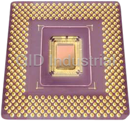
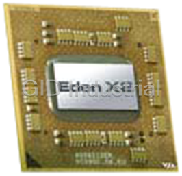
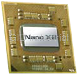
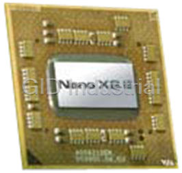


What they say about us
FANTASTIC RESOURCE
One of our top priorities is maintaining our business with precision, and we are constantly looking for affiliates that can help us achieve our goal. With the aid of GID Industrial, our obsolete product management has never been more efficient. They have been a great resource to our company, and have quickly become a go-to supplier on our list!
Bucher Emhart Glass
EXCELLENT SERVICE
With our strict fundamentals and high expectations, we were surprised when we came across GID Industrial and their competitive pricing. When we approached them with our issue, they were incredibly confident in being able to provide us with a seamless solution at the best price for us. GID Industrial quickly understood our needs and provided us with excellent service, as well as fully tested product to ensure what we received would be the right fit for our company.
Fuji
HARD TO FIND A BETTER PROVIDER
Our company provides services to aid in the manufacture of technological products, such as semiconductors and flat panel displays, and often searching for distributors of obsolete product we require can waste time and money. Finding GID Industrial proved to be a great asset to our company, with cost effective solutions and superior knowledge on all of their materials, it’d be hard to find a better provider of obsolete or hard to find products.
Applied Materials
CONSISTENTLY DELIVERS QUALITY SOLUTIONS
Over the years, the equipment used in our company becomes discontinued, but they’re still of great use to us and our customers. Once these products are no longer available through the manufacturer, finding a reliable, quick supplier is a necessity, and luckily for us, GID Industrial has provided the most trustworthy, quality solutions to our obsolete component needs.
Nidec Vamco
TERRIFIC RESOURCE
This company has been a terrific help to us (I work for Trican Well Service) in sourcing the Micron Ram Memory we needed for our Siemens computers. Great service! And great pricing! I know when the product is shipping and when it will arrive, all the way through the ordering process.
Trican Well Service
GO TO SOURCE
When I can't find an obsolete part, I first call GID and they'll come up with my parts every time. Great customer service and follow up as well. Scott emails me from time to time to touch base and see if we're having trouble finding something.....which is often with our 25 yr old equipment.
ConAgra Foods