PROCELERANT™
COM EXPRESS MODULE
PRODUCT MANUAL
CE945GM2A
www.radisys.com
007-02512-0003 September 2008
Release history
Release Date Description
-0000 December 2007 First release.
-0001 July 2007 New CE945GM2A modules and thermal solutions.
-0002 January 2008 New heatsink hardware allows 8mm carrier stack up.
Added tip for reducing EMI on video devices.
-0003 September 2008 Environmental specifications updated.
Copyright © 2006—2008 by RadiSys Technology (Ireland) Ltd. All rights reserved.
Portions of this manual are copyrighted by the PCI Industrial Computer Manufacturers Group, and are reprinted with permission.
RadiSys is a registered trademark and Procelerant is a trademark of RadiSys Corporation. PICMG is a registered trademark and COM
Express is a trademark of the PCI Industrial Computer Manufacturers Group. Intel and Celeron are registered trademarks and Intel Core
is a trademark of Intel Corporation. Micron is a registered trademark of Micron Technology, Inc. Microsoft, Windows, and Windows XP are
registered trademarks of Microsoft Corporation. Red Hat and Red Hat Linux are registered trademarks of Red Hat, Inc. Linux is a
registered trademark of Linus Torvalds. Phoenix is a registered trademark and TrustedCore is a trademark of Phoenix Technologies.
Broadcom is a registered trademark of Broadcom Corporation. Maxtor and DiamondMax are registered trademarks of Maxtor
Corporation. IDT is a registered trademark of Integrated Device Technology, Inc.
All other trademarks, registered trademarks, service marks, and trade names are the property of their respective owners.
TABLE OF CONTENTS
Preface ................................................................................................................................................................ 7
About this manual....................................................................................................................................................................... 7
Safety notices................................................................................................................................................................................ 7
Electrostatic discharge............................................................................................................................................................................7
Where to get more product information ............................................................................................................................... 7
Chapter 1: Product Overview........................................................................................................................... 9
Product products and components......................................................................................................................................... 9
COM Express modules ..........................................................................................................................................................................9
Memory modules ...................................................................................................................................................................................9
Thermal solutions ................................................................................................................................................................................ 10
Module layout .............................................................................................................................................................................10
Chapter 2: Product Specifications ................................................................................................................. 13
Mechanical specifications ........................................................................................................................................................ 13
Module dimensions ............................................................................................................................................................................ 13
Overall assembly dimensions........................................................................................................................................................... 14
Module receptacle............................................................................................................................................................................... 14
Stack-up heights................................................................................................................................................................................... 15
Electrical....................................................................................................................................................................................... 15
Module power consumption ............................................................................................................................................................ 15
Test system configuration ................................................................................................................................15
General Purpose I/O (GPIO) power consumption...................................................................................................................... 17
Thermal specifications...............................................................................................................................................................18
Environmental specifications ...................................................................................................................................................19
Regulatory compliance.............................................................................................................................................................20
EMC compliance .................................................................................................................................................................................. 20
Safety compliance................................................................................................................................................................................ 20
Industry compliance............................................................................................................................................................................ 20
MTBF reliability prediction.......................................................................................................................................................20
3
TABLE OF CONTENTS
Chapter 3: Hardware Reference.................................................................................................................... 21
General specifications............................................................................................................................................................... 21
Block diagram.............................................................................................................................................................................23
Power supply..............................................................................................................................................................................24
Voltage requirements.......................................................................................................................................................................... 24
Inrush current ....................................................................................................................................................................................... 24
CPU...............................................................................................................................................................................................24
Thermal requirements........................................................................................................................................................................ 24
Chipset.........................................................................................................................................................................................25
Graphics and Memory Controller Hub ........................................................................................................................................... 25
I/O Controller Hub .............................................................................................................................................................................. 25
System memory.........................................................................................................................................................................26
Video ............................................................................................................................................................................................26
PCI Express graphics............................................................................................................................................................................ 26
VGA......................................................................................................................................................................................................... 27
LVDS ....................................................................................................................................................................................................... 27
TV-Out .................................................................................................................................................................................................... 27
SDVO ports............................................................................................................................................................................................ 28
Audio............................................................................................................................................................................................28
Storage.........................................................................................................................................................................................28
IDE........................................................................................................................................................................................................... 28
SATA........................................................................................................................................................................................................ 29
I/O.................................................................................................................................................................................................29
General Purpose I/O (GPIO)............................................................................................................................................................. 29
Low-Pinout (LPC)................................................................................................................................................................................. 29
PCI........................................................................................................................................................................................................... 30
PCI Express ............................................................................................................................................................................................ 30
Compatibility with master PCI and PCI Express devices....................................................................................................................... 31
2
SMBus/I C.............................................................................................................................................................................................. 31
Super I/O ............................................................................................................................................................................................... 31
USB ......................................................................................................................................................................................................... 32
4
Ethernet .......................................................................................................................................................................................33
Real-time clock (RTC) ...............................................................................................................................................................33
Flash boot device ......................................................................................................................................................................33
Power management .................................................................................................................................................................34
Advanced Configuration and Power Interface (ACPI) ................................................................................................................. 34
ACPI wake up........................................................................................................................................................................................ 34
System management................................................................................................................................................................35
Intel Virtualization Technology.......................................................................................................................................................... 35
Thermal management..............................................................................................................................................................35
Chapter 4: Thermal Solutions........................................................................................................................ 37
Active heatsinks.......................................................................................................................................................................... 37
Product package contents.................................................................................................................................................................. 37
Mechanical specifications................................................................................................................................................................... 39
Power requirements............................................................................................................................................................................ 40
Passive heatsink .........................................................................................................................................................................40
Product package contents.................................................................................................................................................................. 41
Mechanical specification .................................................................................................................................................................... 41
Heat spreader.............................................................................................................................................................................42
Mechanical specification .................................................................................................................................................................... 42
Thermal interface material application ........................................................................................................................................... 43
Assembly instructions...............................................................................................................................................................43
Thermal interface material application ........................................................................................................................................... 43
Assembly illustrations ......................................................................................................................................................................... 44
Chapter 5: BIOS Configuration and OS Support.........................................................................................45
Boot devices ...............................................................................................................................................................................45
POST and boot process ...........................................................................................................................................................46
Console redirection ............................................................................................................................................................................. 46
BIOS setup.................................................................................................................................................................................. 47
BIOS Update and recovery ..................................................................................................................................................... 47
CMOS save and restore configuration ................................................................................................................................. 47
5
Operating system support.......................................................................................................................................................48
Drivers and utilities ...................................................................................................................................................................48
Appendix A: COM Express Module Pinout Definitions...............................................................................49
CE945GM2A board-to-board interconnector pinouts: type 2.........................................................................................49
COM Express required and optional features ....................................................................................................................55
Appendix B: System Resources...................................................................................................................... 59
PCI resource allocation.............................................................................................................................................................59
Interrupts and GPIOs to carrier board..................................................................................................................................59
BIOS organization and system memory map ....................................................................................................................60
POST checkpoint codes ...........................................................................................................................................................60
POST 80 codes ..................................................................................................................................................................................... 60
TrustedCore BIOS checkpoint codes........................................................................................................................................................ 61
Boot block checkpoint codes ..................................................................................................................................................................... 64
Intel memory initialization checkpoint codes......................................................................................................................................... 65
Error message codes........................................................................................................................................................................... 66
6
PREFACE
About this manual
This manual is written for system engineers who will integrate the Procelerant™ CE945GM2A
COM Express™ embedded computing module into a COM Express carrier board.
For instructions on setting up the CE945GM2A module and a COM Express carrier board, refer
to the Procelerant CE945GM2A COM Express Module Quick Start Guide.
If a custom carrier board will be designed for CE945GM2A modules, you may request RadiSys
for a copy of the Procelerant CE945GM2A COM Express Carrier Board Design Guidelines to
assist in your design process.
Safety notices
Electrostatic discharge
WARNING! This product contains static-sensitive components and should be handled with care.
Failure to employ adequate anti-static measures can cause irreparable damage to components.
Electrostatic discharge (ESD) damage can result in partial or complete device failure,
performance degradation, or reduced operation life. To avoid ESD damage, the following
precautions are strongly recommended.
Keep the COM Express module in its ESD shielding bag until you are ready to install it.
Before touching the COM Express module, attach an ESD wrist strap to your wrist and
connect its other end to a known ground.
Handle the COM Express module only in an area that has its working surfaces, floor
coverings, and chairs connected to a known ground.
Hold the COM Express module only by their edges and mounting hardware. Avoid touching
components and connector pins.
For further information on ESD, visit www.esda.org.
Where to get more product information
Please visit the RadiSys Web site at www.radisys.com for product information and other
resources. Downloads (manuals, release notes, software, etc.) are available via the Technical
Support Library product links at www.radisys.com/support or the product pages at
www.radisys.com/products.
7
Preface
8
PRODUCT OVERVIEW 1
The Procelerant CE945GM2A COM Express module product family is compliant with the
PICMG® COM.0 COM Express Module Base Specification Version 1.0 in the basic form factor.
The CE945GM2A family includes a series of COM Express type 2 modules that uses the Intel®
Calistoga platform with the Yonah processor (Core™ Duo, Core 2 Duo, and Celeron® M),
mobile 945GM Express chipset, and ICH7M Digital Home chipset.
CE945GM2A module features include:
Intel Yonah processor, for faster front side bus, larger L2 cache, lower power, and Intel
Virtualization Technology support
Intel 945GM Express and ICH7M Digital Home chipsets, for faster memory speeds, DDR2
SDRAM, and improved graphics performance
Modular design for reuse, interchangeability, and rapid design updates to meet market
changes, demand fluctuations, and performance upgrades
Product products and components
COM Express modules
Table 1 lists CE945GM2A modules available at the time of production release. All modules are
RoHS-compliant.
Table 1. CE945GM2A product codes
Product code Previous model BGA processor SDRAM SO-DIMM sockets
CE945GM2A-423-0 CE945GM2-423-0 1.06GHz ULV Celeron M 423 None 2
CE945GM2A-L24-0 CE945GM2-L24-0 1.66GHz LV Core Duo L2400 None 2
CE945GM2A-T25-0 CE945GM2-T25-0 2GHz Core Duo T2500 None 2
CE945GM2A-440-0 N/A 1.86GHz Celeron M 440 None 2
CE945GM2A-U25-0 N/A 1.2GHz ULV Core Duo U2500 None 2
CE945GM2A-L74-0 N/A 1.5GHz LV Core 2 Duo L7400 None 2
Memory modules
For a list of DDR2 SO-DIMM SDRAM memory modules validated by RadiSys for use with the
CE945GM2A module, refer to the Procelerant CE945GM2A COM Express Module Qualified
Memory List on the RadiSys Web site.
9
1
Product Overview
Thermal solutions
The CE945GM2-AHS12 active heatsink assembly, CE945GM2-AHS20 active heatsink assembly,
CE945GM2-PHS passive heatsink and CE945GM-HSP heat spreader are specifically designed
for CE945GM modules. See Chapter 4, ”Thermal Solutions” on page 37 for detailed
information.
Module layout
Figure 1. CE945GM2A module layout: top view
DDR2 SO-DIMM
memory sockets
Mobile Intel® 945GM
Express chipset
FWH BIOS flash chip
CPU
Intel® ICH7M Broadcom® BCM5789
Digital Home Ethernet controller
10
1
Module layout
Figure 2. CE945GM2A module layout: bottom view
PCI Express operational
mode switch
Board-to-board
interconnectors
11
1
Product Overview
12
125.00
121.00
80.00
16.50
4.00
0.00
PRODUCT SPECIFICATIONS 2
Mechanical specifications
Module dimensions
The CE945GM2A’s printed circuit board (PCB) is the 125mm x 95mm ”basic module“ size
defined in the PICMG specification. The PCB thickness is 2.5mm.
Figure 3 shows the basic form factor dimensions. The dimension tolerance is ±0.25mm except
that the tolerance of the board-to-board interconnector peg holes (dimensions [16.50, 6.00]
and [16.50, 18.00]) is ±0.10mm.
Figure 3. Basic form factor (in millimeters)
95.00
91.00
91.00
Pin D1
18.00
6.00
4.00
0.00
Pin A1
13
125.00
121.00
85.00
80.00
4.00
.00
2
Product Specifications
Figure 4 shows the dimensions of other holes used to assemble the heatsink and carrier board.
Figure 4. Form factor of CE945GM2A modules
8-MOUNTING HOLE
DRILL SIZE: 2.70
95.00
91.00
50.00
46.00
4.00
.00
Overall assembly dimensions
For overall assembly heights of CE945GM2A modules with each thermal solution, see Chapter
4, ”Thermal Solutions” on page 37.
Module receptacle
The CE945GM2A board-to-board interconnectors use a PICMG-compliant 440-pin module
receptacle (part number: AMP/Tyco 3-1827231-6), comprising two 220-pin, 0.5mm pitch
receptacles.
For pinout definitions of the board-to-board interconnectors and required/optional features for
the corresponding COM Express pinout type, see Appendix A, ”COM Express Module Pinout
Definitions” on page 49.
14
2
Electrical
Stack-up heights
Parts mounted on the bottom surface of the module (between the module and the carrier
board) have a maximum height of 3.8mm. This affects the maximum allowable height of carrier
board components underneath the module.
If the carrier board has module-to-carrier interconnectors 5mm in height, the clearance
between the carrier board and the bottom surface of the module’s PCB is 5mm. This limits
the height of carrier board components underneath the module to 1mm.
If the carrier board has module-to-carrier interconnectors 8mm in height, the clearance
between the carrier board and the bottom surface of the module’s PCB is 8mm. This allows
the use of carrier board components underneath the module up to 4mm in height.
Electrical
Module power consumption
The amount of power consumed by CE945GM modules is highly dependent on the processor,
memory, attached devices, running software, and power state that the module is in. The
following sample measurements were based on the CR100 carrier board and these hardware
configurations:
Power consumption of CE945GM modules includes the power dissipation of CPU and
memory.
Power consumption of the CR100 carrier board includes the power dissipation of the
CR100 carrier board itself, hard disk, PCI-based POST 80 card, USB attachments, and
monitor.
The total system power consumption includes CE945GM modules, CR100 carrier board,
and devices attached onto the CR100 carrier board.
Test system configuration
All tests are done using Intel Thermal Analysis Tool software and Burn In tool under the
following system configuration:
CR100 FlexATX carrier board
Memory: Micron MT16HTF25664HY-667E1, DDR2, 667MHz, CL5, 2GBx2;
Hard disk: Seagate®, ST3160212A, 160GB, PATA
Expansion card: N/A
USB keyboard: Logitech® Y-SJ17
USB mouse: Logitech M-SBF83
Monitor: BENQ® FP737s, LCD
ATX PSU: Seventeam® ST-420BKP-02F
Operating system: Windows XP Professional SP2
15
2
Product Specifications
Table 2. CE945GM2A-423-0 module power rail current consumption
+3.3V +5V +12V +5VSB
Main rail current consumption
Current (A) Current (A) Current (A) Current (A)
Min — — — —
Specification
Max — — 7.5 1.0
Enter DOS (Stable) 0.250 0.100 1.303 0.060
Enter BIOS Setup (Stable) 0.240 0.067 1.298 0.060
At Windows Desktop Idle (Stable) 0.280 0.083 1.028 0.070
Running Windows Stress (Run In) (Max) 0.290 0.085 1.381 0.070
Running CPU Stress (Thermal Analysis Tool) (Max) 0.280 0.083 1.380 0.070
Standby Mode S3 (Stable) 0.000 0.000 0.000 0.150
Hibernate Mode S4 (Stable) 0.000 0.000 0.000 0.060
Power Off S5 (Stable, Wake On LAN enabled) 0.000 0.000 0.000 0.240
Table 3. CE945GM2A-L74-0 module power rail current consumption
+3.3V +5V +12V +5VSB
Main rail current consumption
Current (A) Current (A) Current (A) Current (A)
Min — — — —
Specification
Max — — 7.5 1.0
Enter DOS (Stable) 0.250 0.122 1.580 0.070
Enter BIOS Setup (Stable) 0.250 0.121 1.451 0.070
At Windows Desktop Idle (Stable) 0.280 0.084 0.995 0.070
Running Windows Stress (Run In) (Max) 0.290 0.084 0.995 0.070
Running CPU Stress (Thermal Analysis Tool) (Max) 0.280 0.083 1.894 0.070
Standby Mode S3 (Stable) 0.000 0.000 0.000 0.150
Hibernate Mode S4 (Stable) 0.000 0.000 0.000 0.070
Power Off S5 (Stable, Wake On LAN enabled) 0.000 0.000 0.000 0.240
Table 4. CE945GM2A-U25-0 module power rail current consumption
+3.3V +5V +12V +5VSB
Main rail current consumption
Current (A) Current (A) Current (A) Current (A)
Min — — — —
Specification
Max — — 7.5 1.0
Enter DOS (Stable) 0.240 0.122 1.338 0.070
Enter BIOS Setup (Stable) 0.250 0.070 1.270 0.070
At Windows Desktop Idle (Stable) 0.280 0.084 1.234 0.070
Running Windows Stress (Run In) (Max) 0.290 0.109 1.654 0.070
Running CPU Stress (Thermal Analysis Tool) (Max) 0.280 0.111 1.465 0.070
16
2
Electrical
Table 4. CE945GM2A-U25-0 module power rail current consumption
+3.3V +5V +12V +5VSB
Main rail current consumption
Current (A) Current (A) Current (A) Current (A)
Min — — — —
Specification
Max — — 7.5 1.0
Standby Mode S3 (Stable) 0.000 0.000 0.000 0.150
Hibernate Mode S4 (Stable) 0.000 0.000 0.000 0.060
Power Off S5 (Stable, Wake On LAN enabled) 0.000 0.000 0.000 0.240
Table 5. CE945GM2A-T25-0 module power rail current consumption
+3.3V +5V +12V +5VSB
Main rail current consumption
Current (A) Current (A) Current (A) Current (A)
Min — — — —
Specification
Max — — 7.5 1.0
Enter DOS (Stable) 0.420 0.058 1.730 0.050
Enter BIOS Setup (Stable) 0.420 0.059 1.170 0.050
At Windows Desktop Idle (Stable) 0.450 0.070 1.430 0.060
Running Windows Stress (Run In) (Max) 0.450 0.070 2.380 0.060
Running CPU Stress (Thermal Analysis Tool) (Max) 0.450 0.070 3.120 0.060
Standby Mode S3 (Stable) 0.000 0.000 0.000 0.148
Hibernate Mode S4 (Stable) 0.000 0.000 0.000 0.064
Power Off S5 (Stable, Wake On LAN enabled) 0.000 0.000 0.000 0.250
Wake-On-LAN effect on power dissipation
Table 6 shows an example of the effects of enabling or disabling Wake-on-LAN (WOL) to 5V
standby power dissipation. Actual figures may vary according to your system configuration.
Table 6. Wake-On-LAN effect on system power dissipation
Wake-on-LAN S0 (mA) S3 (mA) Hibernate (mA) S5 (mA)
Enabled 33.00 230.00 210.00 210.00
Disabled 33.00 55.00 35.00 35.00
General Purpose I/O (GPIO) power consumption
Table 7—Table 8 shows the GPIO input and output power for the CE945GM2A module:
GPIO input power consumption
V : Input High Voltage
IH
V : Input Low Voltage
IL
17
2
Product Specifications
GPIO output power consumption
V : Output High Voltage
OH
V : Output Low Voltage
OL
I : Output Low Current
OL
I : Output High Current
OH
Table 7. GPIO input
V V
IH IL
GPIO Name Type
Min Max Min Max
GPI0 Input 2.0V 3.6V -0.5V 0.8V
GPI1 Input 2.0V 3.6V -0.5V 0.8V
GPI2 Input 2.0V 3.6V -0.5V 0.8V
GPI3 Input 2.0V 3.6V -0.5V 0.8V
Table 8. GPIO output
GPIO Name Type V (Min) V (Max) I /I
OH OL OL OH
GPO0 Output 2.3V 0.55V 24mA/-24mA
GPO1 Output 2.3V 0.55V 24mA/-24mA
GPO2 Output 2.8V 0.34V 1.5mA/-0.5mA
GPO3 Output 2.6V 0.4V 6mA/-2mA
Thermal specifications
Table 9 shows the thermal design power (TDP) of the main thermal sources. Note that the TDP
specification is used to design the processor thermal solution. The TDP is not the maximum
theoretical power the processor can dissipate.
Table 9. TDP of main thermal sources
Component TDP
Processor 1.06GHz ULV Celeron M 423 processor 5.5W
1.86GHz Celeron M 440 processor 27W
1.2GHz ULV Core Duo L2400 processor 15W
1.66GHz LV Core Duo U2500 processor 9W
2GHz Core Duo T2500 processor 31W
1.5GHz LV Core 2 Duo L7400 processor 17W
Mobile Intel 945GM Express chipset 7.0W
ICH7M Digital Home chipset 3.3W
Memory Micron DDR2 667 512 MB 5W
Micron DDR2 667 1 GB 6W
Broadcom BCM5789 Ethernet controller 2.5W
Clock generator and others 2W
18
2
Environmental specifications
Environmental specifications
The CE945GM2A meets the following environmental specifications, as tested in a
representative system with 2GB DDR2-400 SDRAM memory installed.
Note: Performance may vary according to the system it is installed in and environmental
conditions. It is particularly important to provide sufficient airflow across CE945GM2A modules
to keep its temperature within the specified operating range.
Characteristic State Value
Temperature Operating 0° C to +60° C, derated 1.1°C per 300m over 2300m
Storage (packaged) –40° C to +85° C, 5° C per minute maximum excursion
(board local ambient)
gradient
Relative humidity Operating 5% to 95% RH non-condensing
95% RH at +30°C, linearly derated to 25% RH at +60°C
Storage (packaged) 5% to 95% RH non-condensing
Altitude Operating Up to 4570 meters
Storage (packaged) Up to 12000 meters
Shock (drop) Operating 30G, half sine, 11ms duration, 3 times per face
Non-operating 40G, half sine, 11ms duration, 3 times per face
(unpackaged)
Vibration Operating Random 5Hz to 2KHz, 7.7grms, 10min in each of 3 axes
2 2
5-20Hz 0.004g /Hz ramping up to 0.04g /Hz
2
20-1000Hz 0.04g /Hz
2 2
1000Hz-2000Hz 0.04g /Hz ramping down to 0.01g /Hz
Non-operating Random 5Hz to 2KHz, 9.7grms, 10min in each of 3 axes
(unpackaged)
2 2
5-20Hz 0.006g /Hz ramping up to 0.06g /Hz
2
20-1000Hz 0.06g /Hz
2 2
1000Hz-2000Hz 0.06g /Hz ramping down to 0.02g /Hz
19
2
Product Specifications
Regulatory compliance
EMC compliance
When correctly installed in a suitable chassis, the CE945GM2A meets these EMC regulations:
EN55022, EN55024
FCC Part 15, Subpart B, Class B
Safety compliance
When correctly installed in a suitable chassis, the CE945GM2A meets these safety regulations:
UL60950, EN60950 and IEC60950
RoHS compliant
Industry compliance
The CE945GM2A meets these industry standards:
IPC-6016 (HDI standard)
European RoHS Directive 2002/95/EC
MTBF reliability prediction
The CE945GM2A has a predicted MTBF of 373,200 hours at 35ºC. The predictions are based
on Telcordia SR-332 Issue 1, Method 1, Case 3 with the following underlying assumptions:
50% default stress ratio for all modeled components
Application-specific stress ratios applied for electrolytic capacitors when available
Ground Benign in a controlled environment
Level II quality grade on all components
Mechanical components are not modeled
No burn-in or pre-testing specified
MTTR specified to be 30 minutes
No component-specific thermal rises or other voltage/current stress applied
+35ºC ambient with 10ºC system level temperature rise assumed
Relex® 7.7 modeling software
20
HARDWARE REFERENCE 3
General specifications
Feature Function Description
Physical Dimensions 125mm x 95mm
COM Express PICMG COM.0 COM Express Basic Specification Revision 1.0 basic form factor,
COM Express type 2 pinouts
Combined 440-pin board-to-board interconnectors comprising two 220-pin,
0.5mm pitch receptacles
Processor BGA options Core Duo, Core 2 Duo, and Celeron M BGA processors
FSB 533/667 MHz
Chipset Intel mobile Intel 945GM Express chipset
Intel ICH7M Digital Home chipset
Memory Type Two 200-pin DDR2 SO-DIMM sockets for up to 4G 400/533/667MHz memory
Capacity 128MB — 4GB
Video Intel integrated chipset graphics supporting dual independent displays
Dual SDVO
18-bit dual-channel LVDS
Analog VGA
TV-Out
One PCI Express x16 graphics interface (lanes [16:31])
Two SDVO interfaces multiplexed with PCI Express x16 graphics interface
Audio One Intel High Definition Audio or AC‘97 Audio interface
One Speaker Out interface
Storage IDE One IDE interface capable of supporting two Ultra ATA/100 devices:
One IDE hard disk drive or CD-ROM/DVD-ROM
One CompactFlash Ultra II, Extreme III, or Extreme IV card
SATA Two SATA interfaces at a normal data transfer rate of up to 1.5Gbps
Support for IDE, AHCI, and RAID (RAID 0 and RAID 1)
21
3
Hardware Reference
Feature Function Description
I/O PCI One 32-bit 33MHz PCI 2.3 interface for four logical devices
PCI Express One PCI Express x14 interface (lanes [0:3]) in configurable options of one x4
interface or four x1 interfaces
One PCI Express x1 interface (lane 4)
PCI Express graphics interface (lanes [16:31]) capable of supporting x1, x2, x4, or
x8 non-graphics device
USB Eight USB 2.0 ports on the COM Express carrier board
Support for USB storage devices: flash drive, ATA hard disk drive, floppy, and
CD-ROM/DVD-ROM
Support for high-speed USB 2.0 Debug Port on each port
Super I/O Support for Winbond WPC8374L Super I/O legacy devices, depending on the
BIOS in use
Support for Winbond W83627EHG SIO Super I/O legacy devices, depending on
the BIOS in use
2 2
I COne I C interface
GPIO Eight GPIO pins (four GPI, four GPO)
Network Single 10/100/1000Mbps Base-T Ethernet
IEEE 802.3 compliant
Programmable Ethernet LEDs for link, activity, and speed
®
BIOS
Phoenix TrustedCore™ BIOS in 1MB Firmware Hub BIOS flash chip
Power Requirement +12V input from carrier board, with + 5V standby (optional)
Management ACPI 3.0 states S0, S3, S4, S5, G3, and C0, C1, C2, C3, C4
Support for ACPI wake up events: power button, RTC alarm, Wake on LAN, and
PCI and PCI Express power management event signaling
OS support Windows® XP® Professional
Windows XP Embedded
Red-Hat® Desktop Linux®
22
3
Block diagram
Block diagram
CK410M
5V_STB_INPUT
CPU
Power supply (VR)
Hardware
monitor
12V_INPUT
VGA
945GM Express
DDR2
Two DDR2 SD-DIMM
TV
(400/533/667)
memory sockets
LVDS
Board-to-board
SDVO or PCIE
interconnectors
graphic optional
DMI
IDE
2 SATA
8 USB
ICH7M Digital Home
5 PCI-E x1
PCI I/F
LPC bus
LPC bus
FWH
HDA
RTC battery 1 PCI-Ex1
To RJ45 Broadcom BCM5789
LAN EEPROM
23
3
Hardware Reference
Power supply
Voltage requirements
The module power comes from the carrier board, and there is a common 3V battery supply for
the real-time clock (RTC).
Table 10. CE945GM2A power supply requirements
Supply Current/Watts DC range Maximum ripple
12V 8.3A/100W 12V ± 5% 100mV @ 0~20MHz
5V standby 1A/1.5W 5V ± 5% 50mV @ 0~20MHz
3V battery 6µA 2.0 — 3.6V —
Inrush current
The inrush current to the module depends on the rise time of the main power from the carrier
board.
Table 11 and Table 12 show the maximum inrush current for the CE945GM2A module.
Table 11. Maximum inrush current with an ATX power supply (12V with +5V
standby)
Measurements
Power rail
Inrush current (A) High voltage (V)
+12V 2.4 11.97
+5 standby 0.644 5.03
Table 12. Maximum inrush current with 12V only power supply
Measurements
Power rail
Inrush current (A) High voltage (V)
+12V 2.6 11.97
CPU
The Intel Yonah processor used on CE945GM2A modules includes the Core Duo, Core 2 Duo,
and Celeron M processors to support different requirements, such as performance, heat
dissipation, space limitations, and voltage needs.
For processor datasheets, visit the Intel Web site, www.intel.com.
Thermal requirements
The processor supports the THERMTRIP# signal for catastrophic thermal protection. An external
thermal sensor is also used to protect the processor and the system against excessive
temperature. If the external thermal sensor detects a catastrophic processor temperature of
125°C (maximum), or if the THERMATRIP# signal is asserted, the voltage supply to the
processor will be turned off within 500ms to prevent permanent silicon damage.
24
3
Chipset
The thermal monitor feature and the thermal control circuit (TCC) will be enabled in the CPU by
the board BIOS. The CPU temperature can be read over the SMBus at any time.
The processor must remain within the minimum and maximum junction temperature (Tj)
specifications at the corresponding thermal design power (TDP) value. For information about Tj
and TDP, see Thermal specifications on page 18.
Chipset
Graphics and Memory Controller Hub
The mobile Intel 945GM Express chipset is a Graphics and Memory Controller Hub (GMCH)
that delivers high-performance, integrated graphics, and manages the flow of information. The
CE945GM2A primarily uses these GMCH interfaces:
533/667MHz FSB interface to the processor. See CPU on page 24 for details.
Single-channel/dual-channel 400/533/667MHz DDR2 memory interface to system
SDRAM. See System memory on page 26 for details.
Graphics interfaces, including the integrated Graphics Media Accelerator (GMA) 950
controller and discrete PCI Express graphics (PEG). See Video on page 26 for details.
Direct media interface (DMI) to the ICH chipset
I/O Controller Hub
The ICH7M Digital Home provides extensive I/O support. The CE945GM2A primarily uses these
ICH features:
PCI Express Base Specification Revision 1.0 support
33 MHz, PCI 2.3 operation support (up to four Req/Gnt pairs)
ACPI power management logic support
Enhanced DMA controller, interrupt controller, and timer functions
SATA host interfaces with independent DMA operation on two ports and AHCI support
IDE interface at a normal transfer rate of Ultra ATA100/66/33
USB host interfaces with support for eight USB2.0 ports
Low Pin Count (LPC) interface
SMBus 2.0 with additional I2C device support
Integrated Gigabit Ethernet controller
Firmware Hub (FWH) interface support
Intel Matrix Storage Technology (RAID 0 and RAID 1) support
Intel High Definition Audio (HDA) support
Intel Virtualization Technology support
25
3
Hardware Reference
System memory
The CE945GM has two 200-pin SO-DIMM sockets to accept 64-bit, non-ECC, non-parity DDR2
memory modules. At least one memory module is required to make the system operational.
System memory interface features include:
Support for 128MB, 256MB, 512MB, 1GB, and 2GB DDR2 SDRAM densities
Support for unbuffered DDR2 SDRAM PC2-3200/PC2-4200/PC2-5300 DDR2 (DDR2-
400/533/667)
Support for memory bus speed of either PC2-3200 (400MHz), PC2-4200 (533MHz), or
PC2-5300 (667MHz)
Support for x8 and x16 DDR2 SDRAM devices
Note: For a list of memory modules that RadiSys has validated for use with CE945GM2A
modules, refer to the Procelerant CE945GM2A COM Express Module Qualified Memory List.
Video
The CE945GM2A is capable of supporting full-precision, floating-point operations of integrated
displays (analog CRT, LVDS interface, TV-out, and SDVO output), discrete PCI Express graphics,
and digital video display if your carrier board has a DVI chipset.
When the system BIOS detects the presence of a PCI Express and/or a PCI graphic card in the
CE945GM2A system, the PCI Express graphics display will be given first priority, then the PCI
graphics display, and finally any integrated displays.
To reduce electromagnetic interference (EMI) on digital video devices and/or LVDS flat panel:
1. During system startup, press to enter the BIOS setup utility.
2. In the Configuration > Video Configuration, enable DVI Spread Spectrum or IGD-LCD
Control > IGD - LVDS Spread Spectrum depending on the video in use.
3. In the Exit menu, save settings and reboot.
PCI Express graphics
The CE945GM2A supports a 16-lane PCI Express interface intended for external PCI Express
graphics cards.
PCI Express graphics features include:
Compliant with the PCI Express Base Specification Revision 1.0-based PCI Express
frequency of 2.5GHz.
Raw bit-rate of 2.5Gbps on each lane while employing 8b/10b encoding to transmit data
across the interface.
Maximum theoretical bandwidth of 4GBps in each direction simultaneously, for an
aggregate bandwidth of 8GBps when using 16 lanes.
26
3
Video
An SDVO graphics display device can also be used in the 16-lane PCI Express slot instead of a
PCI Express graphics card. The slot will support both the SDVO device (multiplexed with SDVO
ports) and a general-purpose PCI Express x1 interface on the PCI Express x16 graphic lanes
[16:31].
Note: The PCI Express x1 and x4 interfaces can also support PCI Express graphics cards.
VGA
The CE945GM2A supports an analog CRT interface via the integrated Intel Graphics Media
Accelerator 950 controller.
VGA interface features include:
Analog CRT DAC interface
DAC frequencies up to 400MHz
24-bit RAMDAC
Analog monitor support up to QXGA (2048x1536)
LVDS
The CE945GM2A supports an LVDS interface via the integrated Intel Graphics Media Accelerator
950 controller.
LVDS interface features include:
Panel resolutions up to UXGA (1600x1200)
25MHz-112MHz single-channel/dual-channel @ 18 bpp — TFT panel type
Pixel dithering for 18-bit TFT panel to emulate 24-bpp true color displays
Panel fitting, panning and center mode
Spread spectrum clocking
Integrated PWM interface for LCD backlight inverter control
TV-Out
The CE945GM2A supports the following TV-Out features via the integrated Intel Graphics Media
Accelerator 950 controller:
Three integrated 10-bit DACs
Overscaling
NTSC/PAL
Component, S-Video and Composite output interfaces
HDTV support for 480p/720p/1080i/1080p
27
3
Hardware Reference
SDVO ports
Two SDVO ports (SDVO B and SDVO C) are multiplexed with the PCI Express x16 interface. See
PCI Express graphics on page 26 for details.
Concurrent operation of x1 PCI Express with SDVO
Two SDVO ports supported
SDVO is multiplexed with PCI Express graphics lanes
DVI 1.0 support for external digital monitor
TV/HDTV/DVD support
Display hot plug support
Supports external SDVO components (DVI, LVDS, and TV-Out)
Support for Procelerant media expansion cards (RadiSys product codes: MEC-DUAL-DVI and
MEC-DUAL-LVDS). For further information, refer to the Procelerant Media Expansion Cards
Product Manual.
Audio
The Intel high definition audio (HDA) specification defines a digital interface that can attach
different types of CODECs, such as audio and modem CODECs. The ICH chipset's HDA digital
link shares pins with the AC-Link. The Intel HDA controller supports up to three CODECs.
To enable or disable HDA or AC‘97 Audio:
1. During system startup, press to enter the BIOS setup utility.
2. In the Configuration > Advanced Configuration menu, disable or allow the system BIOS to
automatically enable the HDA or AC‘97 Audio when detected.
3. In the Exit menu, save settings and reboot.
Storage
IDE
The CE945GM2A provide an IDE interface to attach up to two Ultra ATA/100 devices via the
integrated IDE controller on the ICH chipset. Each IDE device can have independent timings. It
does not consume any legacy DMA resources. The IDE interface integrates 16x32-bit buffers for
optimal transfers.
IDE/ATA interface features include:
Normal data transfer rates up to ATA/100MBps, PIO data transfer rates up to 16MBps, and
Ultra DMA 5
Support for IDE hard disk drive, IDE flash drive, and IDE CD-ROM/DVD-ROM
Support for CompactFlash memory cards
28
3
I/O
To configure IDE devices:
1. During system startup, press to enter the BIOS setup utility.
2. In the Configuration > IDE Configuration > IDE Primary Master/Slave menu, configure
appropriate IDE device settings.
3. In the Exit menu, save settings and reboot.
Note: The system BIOS does not currently support the Ultra DMA operational mode of
CompactFlash memory cards. You can choose the Fast PIO operational mode instead;
otherwise, CompactFlash memory cards may not be detected.
SATA
The ICH chipset has an integrated SATA host controller that supports independent DMA
operation on two ports with data transfer rates of up to 1.5Gbps.
SATA interface features include:
Support for SATA hard disk drives and SATA CD-ROM/DVD-ROM drives
Data transfer rates up to 1.5Gbps
IDE mode
To configure SATA devices:
1. During system startup, press to enter the BIOS setup utility.
2. In the Configuration > IDE Configuration > SATA Port [X] menu, configure appropriate SATA
device settings.
3. In the Exit menu, save settings and reboot.
I/O
General Purpose I/O (GPIO)
Four GPIs [0:3] and four GPOs [0:3] are available via a 20-pin general purpose I/O (GPIO)
header. For GPIO definitions from the ICH chipset through the board-to-board interconnectors
and to the COM Express carrier board, see Interrupts and GPIOs to carrier board on page 59.
Low-Pinout (LPC)
The CE945GM2A supports an LPC interface, which complies with the LPC 1.1 Specification and
supports two master/DMA devices. This interface allows the connection of devices such as
Super I/O, micro controllers, and customer ASICs.
The Port80 Power On Self Test (POST) checkpoint codes can be output to the LPC bus or PCI
bus. For further information, see Chapter 5, ”BIOS Configuration and OS Support” on page 45.
29
3
Hardware Reference
PCI
The CE945GM2A provides a 33MHz, PCI 2.3 bus interface via the integrated PCI controller on
the ICH chipset.
PCI interface features include:
Compliant with the PCI Local Bus Specification Revision 2.3.
Support for up to four PCI devices/slots on the COM Express carrier board. See PCI resource
allocation on page 59 for details.
To configure PCI and PCI Express power management event signaling to wake up the system:
1. During system startup, press to enter the BIOS setup utility.
2. In the Configuration > Power Control Configuration menu, set PME Wake from S5 to
[Enabled].
3. In the Exit menu, save settings and reboot.
PCI Express
The CE945GM2A supports five PCI Express expansion ports (lanes [0:4]) that are compliant
with the PCI Express Base Specification Version 1.1. Each port supports 2.5GBps bandwidth in
each direction (5GBps concurrent).
Lanes [0:3] can be statically configured as one x4 interface or four x1 interfaces via a PCI
Express operational mode switch. See Module layout on page 10 for switch location and
Figure 5 for configuration instructions.
Lane 4 can only be used as one x1 interface.
Figure 5. PCI Express operational mode switch settings
1
2
Setting Description
SW1-1 off & SW1-2 off (default) Enable four independent PCI Express x1 ports
SW1-1 on & SW1-2 on Enable a single PCI Express x4 port
SW1-1 on & SW1-2 off Undefined
SW1-1 off & SW1-2 on Undefined
ON
The system BIOS allows you to disable or enable these PCI Express expansion lanes in the
Configuration > PCI Expansion Slot Configuration menu and if lane 0 is disabled, all other lanes
will be automatically disabled.
To configure PCI Express expansion ports:
1. During system startup, press to enter the BIOS setup utility.
2. In the Configuration > PCI Express Expansion Slot Configuration menu, configure the PCI
Express root ports.
3. In the Exit menu, save settings and reboot.
30
3
I/O
To configure PCI and PCI Express power management event signaling to wake up the system:
4. During system startup, press to enter the BIOS setup utility.
5. In the Configuration > Power Control Configuration menu, set PME Wake from S5 to
[Enabled].
6. In the Exit menu, save settings and reboot.
Compatibility with master PCI and PCI Express devices
When a PCI or PCI Express device communicates with another directly or performs DMA (direct
memory access) to the local memory, bus mastering must be available in the system.
Appropriate drivers for PCI and PCI Express devices are usually used to enable bus mastering
under the operating system.
If drivers are unavailable or do not work as expected, you can use the new BIOS settings to
enable bus mastering. Go into the BIOS setup utility during system startup and enable these
new settings in the Configuration > Advanced Configuration menu:
For access failures, set Force PCI/PCI-E Bus Mastering to [Enabled].
For graphics compatibility problems, set Enhance PCI/PCI-E Software Compatibility to
[Enabled].
2
SMBus/I C
2
The CE945GM2A provides both SMBus and I C buses to the carrier board via the integrated
SMBus 2.0 controller on the ICH chipset. This SMBus controller is compatible with most 2-wire
2
I C compatible devices.
Full access to internal configuration via the SMBus is supported. This allows a server
management card to control the system configuration and read various errors and status
information.
2
Access to the external DIMMs via I C is supported. This is used to determine the nature of
the DIMMs present in order to configure the memory system correctly.
2
For SMBus/I C bus addresses used on the CE945GM2A module, see Figure 6 on page 32.
Super I/O
The CE945GM2A BIOS can support LPC Super I/O legacy devices when a COM Express carrier
board contains a Winbond® WPC8374L or W83627EHG Super I/O chip, depending on the
BIOS in use.
LPC Super I/O legacy devices include:
Serial ports with console redirection
Parallel ports
Floppy disk drives
31
3
Hardware Reference
PS/2 keyboard and mouse
LPT parallel ports
Note: Two BIOS release packages are available on the RadiSys Web site to support these two
Super I/O chips correspondingly, so be sure to find the correct BIOS update packages.
2
Figure 6. CE945GM2A SMBus/I C bus clock diagram
DDR2 SO-DIMM 0
DDR2 SO-DIMM 1
ADDR 1010 000xb
ADDR 1010 010x
ADDR 1010 010xb
Thermal sensor
Clock generator
ADDR 1101 010x
ADDR 1101 001xb
SMBus
ICH7M Digital Home
Board-to-board
Slave ADDR: 1000 000xb
interconnectors
(Programmable by BIOS)
I2C
I2C-bus repeater
Bus
Legend:
Chip
Socket
USB
The CE945GM2A supports eight USB 2.0/1.1 ports [0:7] on a COM Express carrier board via
one Enhanced Host Controller Interface (EHCI) controller and four Universal Host Controller
Interface (UHCI) controllers integrated on the ICH chipset.
USB interface features include:
High-speed, full-speed, and low-speed capable
Support for any type of USB storage devices, such as USB hard disk drive, USB flash drive,
USB floppy disk drive, and USB CD-ROM/DVD-ROM drive
Support for high-speed USB 2.0 Debug Port on each port
32
3
Ethernet
Ethernet
The CE945GM2A supports one 10/100/1000Mbps Ethernet interface via the Broadcom®
BCM5789 Ethernet controller for high-performance networking applications.
Ethernet interface features include:
Gigabit Ethernet support via the PCI Express x1 interface
Integrated PHY for 10/100/1000Mbps full and half-duplex operation
Statistics for SNMP MIB II, Ethernet-like MIB, and Ethernet MIB (802.3z, Clause 30) JTAG
programmable LEDs for link status, traffic, 100Mbps speed, and 1000Mbps speed
ACPI-compliant Wake-on-LAN. See ACPI wake up on page 34 for details.
The Ethernet connection must be active for Wake On LAN. To wake up the system from
Ethernet:
1. During system startup, press to enter the BIOS setup utility.
2. In the Configuration > LAN Configuration menu, enable Onboard LAN and PXE Option
ROM.
3. Be aware that Wake On LAN will become unavailable when Power Saving When S5 is
enabled.
4. In the Exit menu, save settings and reboot.
Tip: When Embedded Ethernet and Option ROM Scan are set to Enabled in the BIOS, you can
press to enter the Broadcom NetXtreme Ethernet Boot Agent utility during system
boot.
Real-time clock (RTC)
The ICH chipset contains a Motorola MC146818A-compatible real-time clock with 256 bytes of
battery-backed RAM. The real-time clock performs two key functions: keeping track of the time
of day and storing system data, even when the system is powered down. The RTC operates on
a 32.768 KHz crystal and a 3 V battery.
To wake up the system from ACPI sleeping states at the specified time:
1. During system startup, press to enter the BIOS setup utility.
2. In the Configuration > Power Configuration menu, set RTC Wake Up to [Enabled] and
specify a value (hour, minute, and second in HH:MM:SS 24-hour clock format) in the Wake-
Up Time item.
3. In the Exit menu, save settings and reboot.
Flash boot device
The CE945GM2A supports an onboard 1MB firmware hub (FWH) BIOS flash chip. The flash
chip is soldered onto the module and cannot be replaced. The BIOS firmware code is stored in
the BIOS flash chip. Based on the Phoenix® TrustedCore™ BIOS with RadiSys extensions, the
33
3
Hardware Reference
CE945GM2A BIOS supports system operation when the CE945GM2A module is used on a
compatible COM Express carrier board. For more information about the BIOS, see Chapter 5,
”BIOS Configuration and OS Support” on page 45.
You can use the BIOS_DISABLE# signal on the carrier board to disable module BIOS ROM and
boot from carrier board BIOS ROM.
Power management
Advanced Configuration and Power Interface (ACPI)
Table 13 shows the ACPI 3.0 power states that CE945GM2A modules support.
Indicates the normal module state in a given VCC state.
* Indicates the states entered by software control via ACPI interfaces.
Table 13. Supported ACPI states for 12V product options
VCC state Supported module states
Description
1 2 3 4 5
5V_SBY 12V
G0/S0 G1/S3 G1/S4 G2/S5 G3
Off Off Power off –––– 9
* *
Off On Carrier board with no standby 9 9* –
9 9
support
On Off Standby – 9 99*–
On On Full power 99* 9* 9*–
1
G0/S0 — Fully operational; working
2
G1/S3 — Standby (Suspend to RAM). Main memory is still powered. This state allows the resumption of work
exactly where it was left at the start of standby.
3
G1/S4 — Non-volatile sleep (Suspend to disk). System context is saved to disk and power removed from all
circuits except those required to resume.
4
G2/S5 — Soft off. All devices are un-powered. Memory contents and context are lost.
5
G3 — Mechanical off. System is un-powered with no standby rails. No wake-up is possible.
ACPI wake up
CE945GM2A modules support these wake-up events from S3, S4, and S5 sleep states:
Power button
RTC alarm. See Real-time clock (RTC) on page 33 for configuration instructions.
Onboard LAN. See Ethernet on page 33 for configuration instructions.
PCI and PCI Express power management event signaling. See PCI on page 30 or PCI
Express on page 30 for configuration instructions.
34
3
System management
System management
Intel Virtualization Technology
The Intel Virtualization Technology (also known as Intel VT) allows a platform to run multiple
operating systems and applications in independent partitions. Functionality, performance and
other benefits will vary depending on hardware and software configurations.
To configure the Intel Virtualization Technology:
1. During system startup, press to enter the BIOS setup utility.
2. In the Configuration > CPU Configuration menu, set VT Feature to [Enabled].
3. In the Exit menu, save settings and reboot.
Thermal management
The processor contains an on-die digital thermal sensor (DTS) to measure the processor
temperature.
The CE945GM2A contains a thermal sensor, National LM99, to measure the module‘s
temperature, which is placed on the top side of the module at location U20. It is an 11-bit digital
temperature sensor with a 2-wire SMBus serial interface. For the SMBus address of this thermal
2
sensor, see SMBus/I C on page 31.
The processor and module temperatures are displayed in the system setup utility during system
boot. To check these temperatures:
4. During system startup, press to enter the BIOS setup utility.
5. In the Information > System Monitors menu, check the temperatures.
6. In the Exit menu, save settings and reboot.
35
3
Hardware Reference
36
THERMAL SOLUTIONS 4
Active heatsinks
The CE945GM2-AHS12 and CE945GM2-AHS20 active heatsink assemblies differ only in the
height of the copper heatsink.
Figure 7. Active heatsink
Active heatsink Thermal performance Use with models Chassis requirement
CE945GM2-AHS12 20W under 60ºC ambient CE945GM2A-423-0 1U or above
environment
(12mm fin height) CE945GM2A-L24-0
CE945GM2A-440-0
CE945GM2A-L74-0
CE945GM2A-U25-0
CE945GM2-AHS20 31W under 60ºC ambient This heatsink is specifically designed for 2U or above
environment CE945GM2A-T25-0 module, but can also be
(20mm fin height)
used on all other modules.
Product package contents
Table 14. CE945GM2-AHS12 contents
Component Description QTY
CE945GM2-AHS12 Active heatsink for CE945GM2-T25-0, 12mm-high fins 1
Heatsink screws M2.5 x16,cross pan head (used to tighten the heatsink and module) 5
Recommended torque 0.45N.m
37
4
Thermal Solutions
Table 14. CE945GM2-AHS12 contents
Component Description QTY
Module screws M2.5 x6, cross pan head (used to attach the heatsink onto the module) 3
Recommended torque 0.45N.m
Carrier screws Used to tighten the carrier board and module: 5/5
For 5mm carrier stack up: M2.5 x4, cross pan head, recommended torque 0.45N.m
For 8mm carrier stack up: M2.5 x7, cross pan head, recommended torque 0.45N.m
Nuts Used with heatsink screws: 5/5
For 5mm carrier stack up: M2.5x5, hex jam, recommended torque 0.5N.m
For 8mm carrier stack up: M2.5x8, hex jam, recommended torque 0.5N.m
Washers M2.5, spring lock (used with heatsink screws) 5
Table 15. CE945GM2-AHS20 contents
Component Description QTY
CE945GM2-AHS20 Active heatsink for CE945GM2-T25-0, 20mm-high fins 1
Heatsink screws M2.5 x16,cross pan head (used to tighten the heatsink and module) 5
Recommended torque 0.45N.m
Module screws M2.5 x6, cross pan head (used to attach the heatsink onto the module) 3
Recommended torque 0.45N.m
Carrier screws Used to tighten the carrier board and module: 5/5
For 5mm carrier stack up: M2.5 x4, cross pan head, recommended torque 0.45N.m
For 8mm carrier stack up: M2.5 x7, cross pan head, recommended torque 0.45N.m
Nuts Used with heatsink screws: 5/5
For 5mm carrier stack up: M2.5x5, hex jam, recommended torque 0.5N.m
For 8mm carrier stack up: M2.5x8, hex jam, recommended torque 0.5N.m
Washers M2.5, spring lock (used with heatsink screws) 5
38
4
Active heatsinks
Mechanical specifications
All dimensions are in millimeters.
Figure 8. CE945GM2-AHS12 and CE945GM2-AHS20 dimensions
117.00
125.00
Figure 9. CE945GM2A with CE945GM2-AHS12 active heatsink
Fin
Fan
13.73
Heatsink cover
4.50
Module PCB
13.00
2.50
39
5X 3.30
87.00
95.00
4
Thermal Solutions
Figure 10. CE945GM2A with CE945GM2-AHS20 active heatsink
Fin
Fan
21.73
4.50
Heatsink cover
13.00 2.50 Module PCB
Power requirements
The active heatsink assemblies require an extra +7.0V — +13.2V power supply (+12V
recommended).
Passive heatsink
The CE945GM2-PHS passive heatsink supports up to 15W thermal dissipation when the
ambient temperature reaches 60ºC. This heatsink is capable of working with CE945GM2A-423-
0, CE945GM2A-L24-0, and CE945GM2A-U25-0 modules in a forced-air cooled chassis that is
at least one rack mount unit (1U) in height.
The forced air must flow across the top of the passive heatsink at a minimum rate of 1.5m/s.
The air must flow in the direction of the heatsink’s fins, as shown in Figure 11.
Figure 11. Airflow over the CE945GM2-PHS passive heatsink
Airflow
40
4
Passive heatsink
Product package contents
Table 16. CE945GM2-PHS contents
Component Description QTY
CE945GM2-PHS Passive heatsink 1
Heatsink screws M2.5 x18.6,cross pan head (used to tighten the heatsink and module) 5
Recommended torque 0.45N.m
Module screws M2.5 x6, cross pan head (used to attach the heatsink onto the module) 3
Recommended torque 0.45N.m
Carrier screws Used to tighten the carrier board and module: 5/5
For 5mm carrier stack up: M2.5 x4, cross pan head, recommended torque 0.45N.m
For 8mm carrier stack up: M2.5 x7, cross pan head, recommended torque 0.45N.m
Nuts Used with heatsink screws: 5/5
For 5mm carrier stack up: M2.5x5, hex jam, recommended torque 0.5N.m
For 8mm carrier stack up: M2.5x8, hex jam, recommended torque 0.5N.m
Washers M2.5, spring lock (used with heatsink screws) 5
Mechanical specification
All dimensions are in millimeters.
Figure 12. CE945GM2-PHS dimensions
117.00
125.00
41
3.30
5X
87.00
95.00
4
Thermal Solutions
Figure 13. CE945GM2A with CE945GM2-PHS passive heatsink
Passive heatsink
31.64 21.90
2.54
Module PCB
Heat spreader
The CEGM452-HSP is compliant with the PIGMG COM.0 COM Express Base Specification
Revision 1.0. This heat spreader is specifically designed as an interface to custom thermal
solutions for all CE945GM2A modules.
This heat spreader can also be used by itself as a thermal solution for the low-power
CE945GM2A-U25-0 COM Express module, where there is a 5W thermal dissipation when the
ambient temperature reaches 60ºC.
Mechanical specification
All dimensions are in millimeters.
117.00
125.00
42
3.30
5X
87.00
95.00
4
Assembly instructions
Thermal interface material application
The thermal interface materials are pre-installed in the same locations as that in the
CE945GM2-PHS passive heatsink. See Figure on page 42 for details. Do not remove the
thermal interface materials.
Assembly instructions
Thermal interface material application
Thermal interface material pads are pre-applied on each heatsink. Heat will be effectively
transferred from the chips to the thermal solution for dissipation. Do not remove the thermal
interface materials.
Figure 14. Thermal interface material pads pre-applied on CE945GM2-AHS12 and CE945GM2-AHS20
Thermagon T-flex 650 gap filler
for GMCH chipset
Thermagon T-pcm 585 phase change material Thermagon T-flex 650
for processor for ICH chipset
43
4
Thermal Solutions
Figure 15. Thermal interface material pads pre-applied on CE945GM2-PHS and CE945GM2-HSP
Thermagon T-flex 500
Thermagon T-flex 500 Thermagon T-flex 500
for memory modules
for GMCH chipset for CPU VR
Benka Y10 phase change material Thermagon T-flex 500 Thermagon T-flex 500
for processor for Ethernet controller for ICH chipset
Assembly illustrations
For detailed instructions on installing the heatsink onto the module and carrier board, refer to
the Quick Start Guide.
44
BIOS CONFIGURATION AND OS SUPPORT 5
The CE945GM BIOS is based on the Phoenix TrustedCore BIOS with RadiSys extensions. BIOS
features include:
Multi-core processing
ACPI 3.0 wake up events from S3, S4, and S5 states, including power button, RTC, Wake On
LAN, and PME wake up
CMOS saving and restoration via system setup utility
Pre-boot Execution Environment (PXE) boot
Port80 Power On Self Test (POST) output to LPC bus or PCI bus
Console redirection to a serial port
USB 2.0 Debug Port on any of eight USB ports
Intel Virtualization Technology
High-resolution, GUI-based, customizable splash screen
Using the BIOS setup utility, you can display and modify the system configurations. The BIOS
configuration is stored in non-volatile CMOS RAM, and is used to initialize the system.
Boot devices
The CE945GM2A BIOS allows you to boot your operating system from any of the following
interfaces and devices:
IDE/ATA
IDE hard disk drive
CompactFlash card
IDE CD-ROM/DVD-ROM
SATA
SATA hard disk drive
SATA CD-ROM/DVD-ROM
USB
USB hard disk drive
USB flash drive
USB floppy drive
USB CD-ROM/DVD-ROM
45
5
BIOS Configuration and OS Support
PXE/Ethernet
To determine the boot device priority:
1. During system startup, press to enter the BIOS setup utility.
2. In the Boot > Boot order menu, select initialization and boot priority for all devices and
actions.
3. In the Exit menu, save settings and reboot.
POST and boot process
The system BIOS performs a Power On Self Test (POST) upon power-on or reset, which tests
and initializes the hardware and programs the chipset and other peripheral components.
When the hardware fails to respond as expected, POST may not be able to continue. For
example, if the memory controller or memory itself cannot be configured, the system cannot
continue to initialize the graphics display because the BIOS-level display driver (also known as
Video BIOS) requires memory to work properly.
The POST attempts to determine whether further operation is possible. Failures during POST
can be indicated by POST checkpoint codes on the BIOS setup screen or POST card that is
installed on the carrier board’s LPC connector. For detailed information, see POST checkpoint
codes on page 60.
After POST completes, the system BIOS performs these steps:
1. Determine whether all boot devices listed in the boot device priority list are operational.
2. Steps through the boot devices and actions in the configured boot order until the system
either loads an operating system successfully. At that point, the system BIOS plays no
further part in the boot process except to provide run-time services to the operating system.
Console redirection
Console redirection is useful especially when your carrier board does not provide a valid video
interface.
To extend video display during system startup, you can use console redirection on a USB port or
on one of the two serial ports if your carrier board includes a Winbond® WPC8374L or
W83627EHG Super I/O chip. Two BIOS release packages are available on the RadiSys Web site
to support these two Super I/O chips correspondingly, so be sure to select the correct BIOS to
support your Super I/O chip.
To set up console redirection:
1. Connect a null modem cable from your host computer to a serial port on your carrier board.
2. During system startup, press to enter the BIOS setup utility.
3. In the Configuration > Advanced Configuration > Legacy Device Configuration menu, set
Console Redirection to the desired serial port.
4. Make sure that Baud Rate, Console Type, Flow Control, and Console Connection are the
same with your host terminal settings.
46
5
BIOS setup
5. Optional. If you need to use console redirection after entering the operating system, set
Continue After POST to [Enabled].
6. In the Exit menu, save settings and reboot.
7. Use a terminal emulation program, such as Windows HyperTerminal, to emulate the video
display.
BIOS setup
To enter the BIOS setup utility, press during system startup. Use the up, down, left, and
right arrow keys on your keyboard to navigate through BIOS items in a menu. Online help is
provided in the system setup screens to explain options.
After you have completed the BIOS settings, press or use the commands on the Exit
menu to save changes. Press to go immediately to the Exit menu.
For detailed instructions on BIOS configuration, refer to the Procelerant CE945GM2A COM
Express Module System Setup utility Specification.
BIOS Update and recovery
BIOS release packages are periodically available on the RadiSys Web site to address known
issues or to add new features. The release packages include detailed instructions for updating
the BIOS.
Note: Two BIOS release packages are available on the RadiSys Web site to support these two
Super I/O chips correspondingly, so be sure to find the correct BIOS update packages.
WARNING! BIOS updates should be undertaken with care and only when necessary. If the BIOS
update is interrupted by a loss of power before it is complete, the BIOS can be corrupted. Recovery
of a corrupted BIOS requires a BIOS recovery diskette. Use the instructions provided with the BIOS
update to make sure the BIOS update is successful.
CMOS save and restore configuration
When you save your settings in the BIOS setup utility, BIOS configurations are saved into the
BIOS CMOS RAM. You can also save the current BIOS settings into the BIOS flash ROM, so that
you can do one of the following later on:
Restore these settings manually as needed
Restore these settings automatically upon CMOS corruption
Restore these settings automatically upon system boot
To save and restore CMOS RAM settings into and from the BIOS flash ROM:
1. Make sure the system is able to boot successfully.
2. During system startup, press to enter the BIOS setup utility.
3. If desired, you can make changes to BIOS settings at this point.
47
5
BIOS Configuration and OS Support
4. In the Exit menu, to save current CMOS items to nonvolatile BIOS flash ROM, move your
cursor to Save CMOS to Flash and press . It will allow you to restore the saved BIOS
configuration after system reboot.
Tip: To erase all previously-stored CMOS data from flash ROM, move your cursor to Erase
CMOS from Flash and press .
5. Optional. To restore the saved BIOS configuration manually, move your cursor to Restore
CMOS from Flash and press .
6. Optional. To restore the saved BIOS configuration automatically upon CMOS corruption or
upon system reboot, set CMOS Restore Condition to [CMOS Corruption] or [Always]
respectively.
7. In the Exit menu, save settings and reboot.
Operating system support
The following operating systems have been validated by RadiSys for CE945GM2A modules:
Windows® XP® Professional
Windows XP Embedded
and Red Hat® Desktop Linux®
For instructions on installing the operating system, refer to the Quick Start Guide.
Drivers and utilities
The operating system you select may require you to install device drivers in order to make the
system operational. Visit the RadiSys Web site for device drivers and utilities.
48
COM EXPRESS MODULE PINOUT DEFINITIONS A
CE945GM2A board-to-board interconnector pinouts: type 2
For general information about the module receptacle, refer to Module receptacle on page 14.
Note: If you are designing a custom carrier board, refer to the COM Express Carrier Board
Design Guidelines for special design instructions.
Table 17. CE945GM2A board-to-board interconnector pinout definitions: type 2
Pin # PICMG definition Pin type Pin # PICMG definition Pin type
A1 GND (FIXED) GROUND B1 GND (FIXED) GROUND
A2 GBE0_MDI3- I/O Analog B2 GBE0_ACT# OD CMOS
A3 GBE0_MDI3+ I/O Analog B3 LPC_FRAME# O CMOS
A4 GBE0_LINK100# OD CMOS B4 LPC_AD0 I/O CMOS
A5 GBE0_LINK1000# OD CMOS B5 LPC_AD1 I/O CMOS
A6 GBE0_MDI2- I/O Analog B6 LPC_AD2 I/O CMOS
A7 GBE0_MDI2+ I/O Analog B7 LPC_AD3 I/O CMOS
A8 GBE0_LINK# OD CMOS B8 LPC_DRQ0# I CMOS
A9 GBE0_MDI1- I/O Analog B9 LPC_DRQ1# I/O CMOS
A10 GBE0_MDI1+ I/O Analog B10 LPC_CLK O CMOS
A11 GND (FIXED) GROUND B11 GND (FIXED) GROUND
A12 GBE0_MDI0- I/O Analog B12 PWRBTN# I CMOS
A13 GBE0_MDI0+ I/O Analog B13 SMB_CK I/O OD CMOS
A14 GBE0_CTREF REF B14 SMB_DAT I/O OD CMOS
A15 SUS_S3# O CMOS B15 SMB_ALERT# I CMOS
A16 SATA0_TX+ O SATA B16 SATA1_TX+ O SATA
A17 SATA0_TX- O SATA B17 SATA1_TX- O SATA
A18 SUS_S4# O CMOS B18 SUS_STAT# O CMOS
A19 SATA0_RX+ I SATA B19 SATA1_RX+ I SATA
A20 SATA0_RX- I SATA B20 SATA1_RX- I SATA
A21 GND (FIXED) GROUND B21 GND (FIXED) GROUND
A22 SATA2_TX+ O SATA B22 SATA3_TX+ O SATA
A23 SATA2_TX- O SATA B23 SATA3_TX- O SATA
A24 SUS_S5# O CMOS B24 PWR_OK I CMOS
A25 SATA2_RX+ I SATA B25 SATA3_RX+ I SATA
A26 SATA2_RX- I SATA B26 SATA3_RX- I SATA
49
A
Table 17. CE945GM2A board-to-board interconnector pinout definitions: type 2
Pin # PICMG definition Pin type Pin # PICMG definition Pin type
A27 BATLOW# I CMOS B27 WDT O CMOS
A28 ATA_ACT# O CMOS B28 AC_SDIN2 I CMOS
A29 AC_SYNC O CMOS B29 AC_SDIN1 I CMOS
A30 AC_RST# O CMOS B30 AC_SDIN0 I CMOS
A31 GND (FIXED) GROUND B31 GND (FIXED) GROUND
A32 AC_BITCLK O CMOS B32 SPKR O CMOS
A33 AC_SDOUT O CMOS B33 I2C_CK O CMOS
A34 BIOS_DISABLE# I CMOS B34 I2C_DAT I/O OD CMOS
A35 THRMTRIP# O CMOS B35 THRM# I CMOS
A36 USB6- I/O USB B36 USB7- I/O USB
A37 USB6+ I/O USB B37 USB7+ I/O USB
A38 USB_6_7_OC# I CMOS B38 USB_4_5_OC# I CMOS
A39 USB4- I/O USB B39 USB5- I/O USB
A40 USB4+ I/O USB B40 USB5+ I/O USB
A41 GND (FIXED) GROUND B41 GND (FIXED) GROUND
A42 USB2- I/O USB B42 USB3- I/O USB
A43 USB2+ I/O USB B43 USB3+ I/O USB
A44 USB_2_3_OC# I CMOS B44 USB_0_1_OC# I CMOS
A45 USB0- I/O USB B45 USB1- I/O USB
A46 USB0+ I/O USB B46 USB1+ I/O USB
A47 VCC_RTC POWER B47 EXCD1_PERST# O CMOS
A48 EXCD0_PERST# O CMOS B48 EXCD1_CPPE# I CMOS
A49 EXCD0_CPPE# I CMOS B49 SYS_RESET# I CMOS
A50 LPC_SERIRQ I/O CMOS B50 CB_RESET# O CMOS
A51 GND (FIXED) GROUND B51 GND (FIXED) GROUND
A52 PCIE_TX5+ O PCIE B52 PCIE_RX5+ I PCIE
A53 PCIE_TX5- O PCIE B53 PCIE_RX5- I PCIE
A54 GPI0 I CMOS B54 GPO1 O CMOS
A55 PCIE_RX4- O PCIE B55 PCIE_RX4+ I PCIE
A56 PCIE_TX4- O PCIE B56 PCIE_RX4- I PCIE
A57 GND GROUND B57 GPO2 O CMOS
A58 PCIE_TX3+ O PCIE B58 PCIE_RX3+ I PCIE
A59 PCIE_TX3- O PCIE B59 PCIE_RX3- I PCIE
A60 GND (FIXED) GROUND B60 GND (FIXED) GROUND
A61 PCIE_TX2+ O PCIE B61 PCIE_RX2+ I PCIE
A62 PCIE_TX2- O PCIE B62 PCIE_RX2- I PCIE
A63 GPI1 I CMOS B63 GPO3 O CMOS
A64 PCIE_TX1+ O PCIE B64 PCIE_RX1+ I PCIE
A65 PCIE_TX1- O PCIE B65 PCIE_RX1- I PCIE
50
A
CE945GM2A board-to-board interconnector pinouts: type 2
Table 17. CE945GM2A board-to-board interconnector pinout definitions: type 2
Pin # PICMG definition Pin type Pin # PICMG definition Pin type
A66 GND GROUND B66 WAKE0# I CMOS
A67 GPI2 I CMOS B67 WAKE1# I CMOS
A68 PCIE_TX0+ O PCIE B68 PCIE_RX0+ I PCIE
A69 PCIE_TX0- O PCIE B69 PCIE_RX0- I PCIE
A70 GND (FIXED) GROUND B70 GND (FIXED) GROUND
A71 LVDS_A0+ O LVDS B71 LVDS_B0+ O LVDS
A72 LVDS_A0- O LVDS B72 LVDS_B0- O LVDS
A73 LVDS_A1+ O LVDS B73 LVDS_B1+ O LVDS
A74 LVDS_A1- O LVDS B74 LVDS_B1- O LVDS
A75 LVDS_A2+ O LVDS B75 LVDS_B2+ O LVDS
A76 LVDS_A2- O LVDS B76 LVDS_B2- O LVDS
A77 LVDS_VDD_EN O LVDS B77 LVDS_B3+ O LVDS
A78 LVDS_A3+ O LVDS B78 LVDS_B3- O LVDS
A79 LVDS_A3- O LVDS B79 LVDS_BKLT_EN O LVDS
A80 GND (FIXED) GROUND B80 GND (FIXED) GROUND
A81 LVDS_A_CK+ O LVDS B81 LVDS_B_CK+ O LVDS
A82 LVDS_A_CK- O LVDS B82 LVDS_B_CK- O LVDS
A83 LVDS_I2C_CK O LVDS B83 LVDS_BKLT_CTRL O CMOS
A84 LVDS_I2C_DAT O LVDS B84 VCC_5V_SBY POWER
A85 GPI3 I CMOS B85 VCC_5V_SBY POWER
A86 KBD_RST# I CMOS B86 VCC_5V_SBY POWER
A87 KBD_A20GATE I CMOS B87 VCC_5V_SBY POWER
A88 PCIE0_CK_REF+ O CMOS B88 RSVD RSVD
A89 PCIE0_CK_REF- O CMOS B89 VGA_RED O Analog
A90 GND (FIXED) GROUND B90 GND (FIXED) GROUND
A91 RSVD RSVD B91 VGA_GRN O Analog
A92 RSVD RSVD B92 VGA_BLU O Analog
A93 GPO0 O CMOS B93 VGA_HSYNC O CMOS
A94 RSVD RSVD B94 VGA_VSYNC O CMOS
A95 RSVD RSVD B95 VGA_I2C_CK O CMOS
A96 GND GROUND B96 VGA_I2C_DAT I/O OD CMOS
A97 VCC_12V POWER B97 TV_DAC_A O Analog
A98 VCC_12V POWER B98 TV_DAC_B O Analog
A99 VCC_12V POWER B99 TV_DAC_C O Analog
A100 GND (FIXED) GROUND B100 GND (FIXED) GROUND
A101 VCC_12V POWER B101 VCC_12V POWER
A102 VCC_12V POWER B102 VCC_12V POWER
A103 VCC_12V POWER B103 VCC_12V POWER
A104 VCC_12V POWER B104 VCC_12V POWER
51
A
Table 17. CE945GM2A board-to-board interconnector pinout definitions: type 2
Pin # PICMG definition Pin type Pin # PICMG definition Pin type
A105 VCC_12V POWER B105 VCC_12V POWER
A106 VCC_12V POWER B106 VCC_12V POWER
A107 VCC_12V POWER B107 VCC_12V POWER
A108 VCC_12V POWER B108 VCC_12V POWER
A109 VCC_12V POWER B109 VCC_12V POWER
A110 GND (FIXED) GROUND B110 GND (FIXED) GROUND
C1 GND (FIXED) GROUND D1 GND (FIXED) GROUND
C2 IDE_D7 I/O CMOS D2 IDE_D5 I/O CMOS
C3 IDE_D6 I/O CMOS D3 IDE_D10 I/O CMOS
C4 IDE_D3 I/O CMOS D4 IDE_D11 I/O CMOS
C5 IDE_D15 I/O CMOS D5 IDE_D12 I/O CMOS
C6 IDE_D8 I/O CMOS D6 IDE_D4 I/O CMOS
C7 IDE_D9 I/O CMOS D7 IDE_D0 I/O CMOS
C8 IDE_D2 I/O CMOS D8 IDE_REQ I CMOS
C9 IDE_D13 I/O CMOS D9 IDE_IOW# O CMOS
C10 IDE_D1 I/O CMOS D10 IDE_ACK# O CMOS
C11 GND (FIXED) GROUND D11 GND (FIXED) GROUND
C12 IDE_D14 I/O CMOS D12 IDE_IRQ I CMOS
C13 IDE_ICRDY I CMOS D13 IDE_A0 O CMOS
C14 IDE_IOR# O CMOS D14 IDE_A1 O CMOS
C15 PCI_PME# I CMOS D15 IDE_A2 O CMOS
C16 PCI_GNT2# O CMOS D16 IDE_CS1# O CMOS
C17 PCI_REQ2# I CMOS D17 IDE_CS3# O CMOS
C18 PCI_GNT1# O CMOS D18 IDE_RESET# O CMOS
C19 PCI_REQ1# I CMOS D19 PCI_GNT3# O CMOS
C20 PCI_GNT0# O CMOS D20 PCI_REQ3# I CMOS
C21 GND (FIXED) GROUND D21 GND (FIXED) GROUND
C22 PCI_REQ0# I CMOS D22 PCI_AD1 I/O CMOS
C23 PCI_RESET# GROUND D23 PCI_AD3 I/O CMOS
C24 PCI_AD0 I/O CMOS D24 PCI_AD5 I/O CMOS
C25 PCI_AD2 I/O CMOS D25 PCI_AD7 I/O CMOS
C26 PCI_AD4 I/O CMOS D26 PCI_C/BE0# I/O CMOS
C27 PCI_AD6 I/O CMOS D27 PCI_AD9 I/O CMOS
C28 PCI_AD8 I/O CMOS D28 PCI_AD11 I/O CMOS
C29 PCI_AD10 I/O CMOS D29 PCI_AD13 I/O CMOS
C30 PCI_AD12 I/O CMOS D30 PCI_AD15 I/O CMOS
C31 GND (FIXED) GROUND D31 GND (FIXED) GROUND
C32 PCI_AD14 I/O CMOS D32 PCI_PAR I/O CMOS
C33 PCI_C/BE1# I/O CMOS D33 PCI_SERR# I/O OD CMOS
52
A
CE945GM2A board-to-board interconnector pinouts: type 2
Table 17. CE945GM2A board-to-board interconnector pinout definitions: type 2
Pin # PICMG definition Pin type Pin # PICMG definition Pin type
C34 PCI_PERR# I/O CMOS D34 PCI_STOP# I/O CMOS
C35 PCI_LOCK# I/O CMOS D35 PCI_TRDY# I/O CMOS
C36 PCI_DEVSEL# I/O CMOS D36 PCI_FRAME# I/O CMOS
C37 PCI_IRDY# I/O CMOS D37 PCI_AD16 I/O CMOS
C38 PCI_C/BE2# I/O CMOS D38 PCI_AD18 I/O CMOS
C39 PCI_AD17 I/O CMOS D39 PCI_AD20 I/O CMOS
C40 PCI_AD19 I/O CMOS D40 PCI_AD22 I/O CMOS
C41 GND (FIXED) GROUND D41 GND (FIXED) GROUND
C42 PCI_AD21 I/O CMOS D42 PCI_AD24 I/O CMOS
C43 PCI_AD23 I/O CMOS D43 PCI_AD26 I/O CMOS
C44 PCI_C/BE3# I/O CMOS D44 PCI_AD28 I/O CMOS
C45 PCI_AD25 I/O CMOS D45 PCI_AD30 I/O CMOS
C46 PCI_AD27 I/O CMOS D46 PCI_IRQC# I CMOS
C47 PCI_AD29 I/O CMOS D47 PCI_IRQD# I CMOS
C48 PCI_AD31 I/O CMOS D48 PCI_CLKRUN# I/O CMOS
C49 PCI_IRQA# I CMOS D49 PCI_M66EN I CMOS
C50 PCI_IRQB# I CMOS D50 PCI_CLK O CMOS
C51 GND (FIXED) GROUND D51 GND (FIXED) GROUND
C52 PEG_RX0+ I PCIE D52 PEG_TX0+ O PCIE
C53 PEG_RX0- I PCIE D53 PEG_TX0- O PCIE
C54 TYPE0# PDS D54 PEG_LANE_RV# I CMOS
C55 PEG_RX1+ I PCIE D55 PEG_TX1+ O PCIE
C56 PEG_RX1- I PCIE D56 PEG_TX1- O PCIE
C57 TYPE1# PDS D57 TYPE2# PDS
C58 PEG_RX2+ I PCIE D58 PEG_TX2+ O PCIE
C59 PEG_RX2- I PCIE D59 PEG_TX2- O PCIE
C60 GND (FIXED) GROUND D60 GND (FIXED) GROUND
C61 PEG_RX3+ I PCIE D61 PEG_TX3+ O PCIE
C62 PEG_RX3- I PCIE D62 PEG_TX3- O PCIE
C63 RSVD RSVD D63 RSVD RSVD
C64 RSVD RSVD D64 RSVD RSVD
C65 PEG_RX4+ I PCIE D65 PEG_TX4+ O PCIE
C66 PEG_RX4- I PCIE D66 PEG_TX4- O PCIE
C67 RSVD RSVD D67 GND GROUND
C68 PEG_RX5+ I PCIE D68 PEG_TX5+ O PCIE
C69 PEG_RX5- I PCIE D69 PEG_TX5- O PCIE
C70 GND (FIXED) GROUND D70 GND (FIXED) GROUND
C71 PEG_RX6+ I PCIE D71 PEG_TX6+ O PCIE
C72 PEG_RX6- I PCIE D72 PEG_TX6- O PCIE
C73 SDVO_DATA I/O OD CMOS D73 SDVO_CLK O CMOS
53
A
Table 17. CE945GM2A board-to-board interconnector pinout definitions: type 2
Pin # PICMG definition Pin type Pin # PICMG definition Pin type
C74 PEG_RX7+ I PCIE D74 PEG_TX7+ O PCIE
C75 PEG_RX7- I PCIE D75 PEG_TX7- O PCIE
C76 GND GROUND D76 GND GROUND
C77 RSVD RSVD D77 IDE_CBLID# I CMOS
C78 PEG_RX8+ I PCIE D78 PEG_TX8+ O PCIE
C79 PEG_RX8- I PCIE D79 PEG_TX8- O PCIE
C80 GND (FIXED) GROUND D80 GND (FIXED) GROUND
C81 PEG_RX9+ I PCIE D81 PEG_TX9+ O PCIE
C82 PEG_RX9- I PCIE D82 PEG_TX9- O PCIE
C83 RSVD RSVD D83 RSVD RSVD
C84 GND GROUND D84 GND GROUND
C85 PEG_RX10+ I PCIE D85 PEG_TX10+ O PCIE
C86 PEG_RX10- I PCIE D86 PEG_TX10- O PCIE
C87 GND GROUND D87 GND GROUND
C88 PEG_RX11+ I PCIE D88 PEG_TX11+ O PCIE
C89 PEG_RX11- I PCIE D89 PEG_TX11- O PCIE
C90 GND (FIXED) GROUND D90 GND (FIXED) GROUND
C91 PEG_RX12+ I PCIE D91 PEG_TX12+ O PCIE
C92 PEG_RX12- I PCIE D92 PEG_TX12- O PCIE
C93 GND GROUND D93 GND GROUND
C94 PEG_RX13+ I PCIE D94 PEG_TX13+ O PCIE
C95 PEG_RX13- I PCIE D95 PEG_TX13- O PCIE
C96 GND GROUND D96 GND GROUND
C97 RSVD RSVD D97 PEG_ENABLE# I CMOS
C98 PEG_RX14+ I PCIE D98 PEG_TX14+ O PCIE
C99 PEG_RX14- I PCIE D99 PEG_TX14- O PCIE
C100 GND (FIXED) GROUND D100 GND (FIXED) GROUND
C101 PEG_RX15+ I PCIE D101 PEG_TX15+ O PCIE
C102 PEG_RX15- I PCIE D102 PEG_TX15- O PCIE
C103 GND GROUND D103 GND GROUND
C104 VCC_12V POWER D104 VCC_12V POWER
C105 VCC_12V POWER D105 VCC_12V POWER
C106 VCC_12V POWER D106 VCC_12V POWER
C107 VCC_12V POWER D107 VCC_12V POWER
C108 VCC_12V POWER D108 VCC_12V POWER
C109 VCC_12V POWER D109 VCC_12V POWER
C110 GND (FIXED) Ground D110 GND (FIXED) GROUND
54
A
COM Express required and optional features
COM Express required and optional features
Required and optional features for COM Express module pinouts type 1 and type 2 are
summarized in Table 18:
Features identified as Minimum (Min) must be implemented by all COM Express modules.
Features identified as Maximum (Max) may be additionally implemented by a COM Express
module.
The upper row symbol (↑) indicates that the corresponding cell has the same instructions
as the upper cell does.
Table 18. Module pinout type 2 — Required and optional features
COM Express interfaces Min/Max Note
System I/O
PCI Express Graphics (PEG) 0/1 These signals may be multiplexed with SDVO signals or
defined as ordinary PCI Express signals. The PEG lanes are the
same lanes as PCI Express lanes 16-31.
PCI Express lanes 0 - 5 2/6 ↑
PCI Express lanes 6-15 N/A ↑
PCI Express lanes 16-31 0/16 ↑
(same as PEG pins)
SDVO channels 0/2 Serial Digital Video Output to LVDS or TMDS transmitters on
the carrier board.
These signals, if implemented, shall be multiplexed with PEG
signals.
LVDS channels 0/2 Low voltage differential signaling flat-panel interface. The
module pinout allows two single channel display interfaces
(each with 1 pixel per clock) with up to 24 bits per color.
Alternatively, one dual channel display (2 pixels per clock) with
up to 24 bits per color, 48 bits per clock is allowed.
Includes panel backlight control and EDID support.
VGA port 0/1 Analog RGB interface for CRT monitor and DDC support.
TV-Out 0/1 If TV-Out is supported, then Composite Video shall be
available.
Component and S-Video may also be available.
PATA port 1/1 Parallel ATA support for up to 2 devices in a master/slave
configuration. This signaling interface is limited to ATA100
speeds. Higher (ATA133) speeds are not defined.
PATA signal pins are reused in pinout type 3 and 5 modules for
2 additional Gigabit Ethernet interfaces.
55
A
Table 18. Module pinout type 2 — Required and optional features (Continued)
COM Express interfaces Min/Max Note
SATA / SAS ports 2/4 Serial ATA links for support of existing SATA-150 and emerging
SATA-300 devices. Alternatively, this interface may be used for
Serial Attached SCSI (SAS).
SAS operation may be indicated by a byte in the Carrier Board
configuration EEPROM.
AC’97 digital interface 0/1 The AC ‘97 audio CODEC interface is limited to support a
single AC‘97 link.
High Definition Audio may be supported.
USB 2.0 ports 4/8 All USB interfaces shall be USB 2.0 compliant. The minimum of
4 USB channels provides support for keyboard, mouse, CD/
DVD drive, and one additional device.
Note that this usage is not required and the actual carrier
usage of the USB port is undefined in the PICMG specification.
LAN 0 (10/100Base-T min) 1/1 Up to 3 Gigabit Ethernet ports are defined, designated GBE0
through GBE2. The ports may operate in 10, 100, or 1000 Mbit/
s modes. The ports are analog-encoded GBE signals, post PHY
but without isolation magnetics. Magnetics are assumed to be
on the carrier board.
All COM Express modules shall implement at least one 10/100
Ethernet port on the GBE0 pin slot. Ports GBE1 and GBE2 may
be combined to form a 10 Gigabit / sec Ethernet interface.
LAN 1 (10/100Base-T min) N/A ↑
LAN 2 (10/100Base-T min) N/A ↑
PCI bus - 32 bit 1/1 The PCI bus interface is specified to be a 32-bit PCI 2.3
compliant bus with speed options of 33MHz or 66MHz.
ExpressCard support 1/2 ExpressCard is a small form factor expansion card for mobile
systems that uses PCI Express or USB as the interface. It is
similar in concept and scope to CardBus. COM Express
modules shall provide support functions for at least one
ExpressCard.
This does not mean that a module PCI Express lane or USB link
are specifically allocated to ExpressCard use, but it does mean
that the module pins for ExpressCard detection and support
are present.
LPC bus 1/1 The LPC bus provides legacy I/O support on a carrier board via
a Super I/O and system management devices.
System management
GPIs 4/4 GPI and GPO pins may be implemented as GPIO (module
specific).
GPOs 4/4 ↑
56
A
COM Express required and optional features
Table 18. Module pinout type 2 — Required and optional features (Continued)
COM Express interfaces Min/Max Note
SMBus 1/1 The SMBus port is specified for system management functions.
It is used on the module to manage system functions such as
reading the DRAM SPD EEPROM and setting clock synthesizer
parameters. Off module, the SMBus should be used carefully.
SMBus may be useful for implementation of standards such as
Smart Battery on the carrier board.
2 2
1/1
I C The I C port shall be available in addition to the SMBus.
Watchdog timer 0/1 COM Express modules may implement a watchdog timer
output to the carrier board.
For further information about watchdog timer output design,
refer to the PICMG specification.
Speaker out 1/1 This port provides the PC beep signal, which is typically used
for debugging purposes.
External BIOS ROM support 0/1 A module pin, BIOS_DISABLE#, may be provided by the
module hardware.
If the function is supported, then the carrier board may pull the
BIOS_DISABLE# pin low to disable the on-module BIOS ROM,
allowing the module to boot from a BIOS ROM on the carrier
board.
Reset functions 1/1 This function includes reset signals to and from the module:
Signals SYS_RESET#, CB_RESET# and KBD_RST# shall be
supported for all module pinout types.
Signal PCI_RESET# shall be supported for pinout types 2
and 3.
Signal IDE_RESET# shall be supported for pinout types 2
and 4.
Signal PWR_OK should be an input term that keeps the
module in a reset condition if low.
Power management
Thermal protection 0/1 This port provides thermal signaling to protect critical
components on the module and the carrier board.
Battery-low alarm 0/1 This port provides a battery-low signal to the module for
orderly transition to power saving or power cut-off ACPI
modes.
Suspend 0/1 This port defines the signaling to indicate that the module has
entered the ACPI power-saving mode S3 (Suspend-To-RAM or
STR), S4 (Suspend-To-Disk or STD), or S5 (Soft-Off).
Wake 0/2 This port defines the signaling to wake up the module from a
power saving mode.
Most prevalent choices for these signals are RING# and LID#,
although other choices can be implemented.
57
A
Table 18. Module pinout type 2 — Required and optional features (Continued)
COM Express interfaces Min/Max Note
Power button support 1/1 This port defines the signaling for powering down the module.
Power good 1/1 This port defines the signaling for the correct power conditions
to proceed with normal startup of the module.
58
SYSTEM RESOURCES B
PCI resource allocation
Slot / Device Signal Slot / Device 0 Slot / Device 1 Slot / Device 2 Slot / Device 3
IDSEL PCI_AD[20] PCI_AD[21] PCI_AD[22] PCI_AD[23]
PCI Clock PCI_CLK replica PCI_CLK replica PCI_CLK replica PCI_CLK replica
INTA# PCI_IRQ[A]# PCI_IRQ[B]# PCI_IRQ[C]# PCI_IRQ[D]#
INTB# (if used) PCI_IRQ[B]# PCI_IRQ[C]# PCI_IRQ[D]# PCI_IRQ[A]#
INTC# (if used) PCI_IRQ[C]# PCI_IRQ[D]# PCI_IRQ[A]# PCI_IRQ[B]#
INTD# (if used) PCI_IRQ[D]# PCI_IRQ[A]# PCI_IRQ[B]# PCI_IRQ[C]#
REQ0# (if used) PCI_REQ[0]# PCI_REQ[1]# PCI_REQ[2]# PCI_REQ[3]#
REQ1# (if used) PCI_REQ[1]# PCI_REQ[2]# PCI_REQ[3]# PCI_REQ[0]#
REQ2# (if used) PCI_REQ[2]# PCI_REQ[3]# PCI_REQ[0]# PCI_REQ[1]#
REQ3# (if used) PCI_REQ[3]# PCI_REQ[0]# PCI_REQ[1]# PCI_REQ[2]#
GNT0# (if used) PCI_GNT[0]# PCI_GNT[1]# PCI_GNT[2]# PCI_GNT[3]#
GNT1# (if used) PCI_GNT[1]# PCI_GNT[2]# PCI_GNT[3]# PCI_GNT[0]#
GNT2# (if used) PCI_GNT[2]# PCI_GNT[3]# PCI_GNT[0]# PCI_GNT[1]#
GNT3# (if used) PCI_GNT[3]# PCI_GNT[0]# PCI_GNT[1]# PCI_GNT[2]#
Interrupts and GPIOs to carrier board
Pin # Pin name Chipset definition
A54 GPI0 GPIO6
A63 GPI1 GPIO7
A67 GPI2 GPIO38
A85 GPI3 GPIO39
A93 GPO0 GPIO17
B54 GPO1 GPIO33
B57 GPO2 GPIO34
B63 GPO3 GPIO35
59
B
BIOS organization and system memory map
Range Description Cacheable
0 to 640 KB 0000 0000 0009 FFFF DOS Compatibility Area Yes
640 KB to 1 MB 000A 0000 000B FFFF Legacy Video DRAM, mapped to the No
video module (SMM Memory) 128 K
000C 0000 000C BFFF Write-protected DRAM containing Yes
shadowed video BIOS (48 KB)
1
000D 0000 000D FFFF BIOS extensions
Yes
000E 0000 000F FFFF System BIOS shadow Yes
2
1 MB to 512 MB 0010 0000 0FFF FFFF DRAM (511 MB)
Yes
512 MB to Top 1000 0000 FFEF FFFF ISA bus (aliased) No
1 MB
Top 1 MB FFF0 0000 FFFF FFFF System ROM (1MB Flash Boot Device) No
1
If no BIOS extensions and ISA bus (aliased), not cacheable.
2
If no DRAM and ISA bus (aliased), not cacheable.
POST checkpoint codes
POST 80 codes
This section lists the POST checkpoint codes that the system BIOS may send to I/O port 80h
during POST. They are presented in an alphabetically ascending order and are not necessarily in
order of execution.
If an error occurs at any of the listed checkpoints, the system attempts to generate beeps to
indicate where the error occurred. To hear the beeps, connect a speaker (not included) to the
speaker pin on the front panel I/O header. Beep codes are derived from the checkpoint code in
the following way:
1. The 8-bit hexadecimal checkpoint code is converted to binary, then the binary number is
divided into four 2-bit groups. For example:
Checkpoint code 20h = 00100000 = 00-10-00-00
2. Each 2-bit group is converted to a one-based number, and 1 is added to indicate the
number of beeps:
3. 00 10 00 00 = 1-3-1-1 beeps
Note: Only standard Phoenix TrustedCore BIOS POST 80 codes are listed in the tables below. If
you encounter other POST 80 codes, contact RadiSys for further assistance.
60
B
POST checkpoint codes
TrustedCore BIOS checkpoint codes
Checkpoint code Description
01h IPMI Initialization.
02h Verifies that CPU is in real mode from cold start.
03h Disables NMIs.
04h Gets CPU type from CPU registers.
06h Miscellaneous hardware initialization.
07h Disables system ROM shadow and start to execute from the flash device.
08h Initializes chipset registers to power-on defaults.
09h Sets In-POST bit in CMOS.
0Ah Completes any implementation-specific CPU initialization.
0Bh Enables L1 cache during POST.
0Ch Initializes cache(s).
0Fh Disables IDE operation.
11h Alternates register initialization.
12h Restores contents of CR0 following CPU reset
13h Resets PCI devices in early post.
14h Initializes and configures the keyboard controller.
16h Verifies ROM BIOS checksum.
17h Initializes external cache before memory auto size.
18h Initializes the timers.
1Ah Tests the DMA registers.
1Ch Initializes interrupt controllers for some shutdowns.
20h Verifies DRAM refresh.
22h Initializes the Keyboard Controller for Keyboard Test.
24h Sets 4GB segments for DS,ES,FS,GS,SS.
28h Sizes DRAM.
29h Initializes the POST Memory Manager.
2Ah Zeroes the RAM up to the minimum RAM specified in the chipset RAM table.
2Ch Tests address lines of the RAM.
2Eh Tests the first 4MB of RAM.
2Fh Initializes external cache before shadowing.
32h Computes CPU clock speed in MHz.
33h Initializes the Phoenix Dispatch Manager.
34h Tests the CMOS RAM and RTC (S2D)
36h Vector to the proper shutdown routine.
38h Shadows system BIOS ROM.
3Ah Auto sizes the external cache.
3Bh Debugs Service init.
61
B
Checkpoint code Description
3Ch Advanced chipset configuration.
3Dh Alternates register configuration.
42h Initializes interrupt vectors.
45h POST device initialization.
46h Verifies that the copyright message is intact.
48h Verifies the hardware configuration and note whether we have color or monochrome
video.
4Ah Initializes the video device.
4Bh Initializes QuietBoot (splash screen).
4Ch Shadows video BIOS ROM.
4Eh Displays the copyright message.
4Fh Allocates storage for Multiboot tables.
50h Displays the CPU type and speed.
52h Initializes and Configures the Keyboard & PS/2 Mouse.
55h Configures USB devices.
58h Tests hot interrupts
59h Initializes the POST display service.
5Ah Displays “Press F2 for Setup“ prompt.
5Bh Disables L1 cache.
5Ch Determines size of conventional memory.
60h Performs memory tests on extended RAM.
62h Preforms address tests on extended RAM.
66h Configures MTRR for extended memory caching.
67h Initializes the non-primary processors.
68h Enables cache(s).
69h Initializes SMM, SMRAM and SMI code.
6Ah Displays cache size.
6Ch Displays BIOS shadow status.
6Eh Zeroes un-initialized extended memory with cache on.
70h Displays any errors found.
72h Checks bad configuration.
76h Reports if there was a Keyboard or Controller failures.
7Ch Initializes hardware interrupt vectors.
7Eh Coprocessor initialization.
81h POST device initialization.
82h Initializes RS232 devices.
83h Configures non-MCD IDE controllers.
84h Initializes Parallel port(s).
85h Configures PC Compatible Plug and Play ISA devices.
87h Initializes MCDs (motherboard configurable devices).
62
B
POST checkpoint codes
Checkpoint code Description
88h Initializes time-outs, key buffer, soft reset flag, and shadow RAM.
89h Enables NMIs.
8Ah Initializes extended BIOS data area.
8Bh Sets up PS/2 mouse interrupt & initialize extended BDA.
8Ch Initializes legacy floppy disk drive(s).
90h Tests hard disks.
91h Programs timing registers according to PIO modes.
93h Creates MP tables.
95h Tests CDROM.
96h Exits big real mode.
97h Fixes up the MP table physical pointer and checksum.
98h Configures non-PC-compatible Plug and Play ISA devices, PCI IRQs, enable PCI devices and
ROM-scan.
99h Checks SMART status.
9Ch Late SMM (system memory mode) initialization.
9Dh Initializes the system security engine.
9Eh Enables the proper hardware interrupts.
A0h Sets time of day.
A2h Tests if key lock or keyboard controller password is on.
A8h Removes the “Press F2 for Setup“ prompt.
AAh Checks if User has requested to enter setup.
ACh Checks to see if setup should be executed.
AEh Clears ConfigFailedBit and InPostBit in CMOS.
B0h Checks for POST errors.
B2h Clears CMOS bits to indicate that POST is complete.
B3h Stores enhanced CMOS values in non-volatile area.
B5h Terminates QuietBoot (splash screen).
B6h Queries for password before boot.
B7h Configures ACPI tables for OS usage.
B9h Prepares to boot.
BAh Executes DMI handlers.
BCh Clears the parity error latch, set correct NMI state.
BDh Displays the “boot first“ menu.
BEh Clears the screen.
BFh Checks the reminder features (virus, backup).
C0h Boots the operating system via Int19.
C1h Initializes PEM (Phoenix Error Manager) data structures
C2h Saves the current boot type into CMOS.
C2h Invokes error logging function for all registered error handlers.
C3h Checks the requested boot type.
63
B
Checkpoint code Description
C3h Invokes error handler(s) for asserted errors.
C4h Initializes (clears) the system error flags.
C4h Installs the IRQ1 vector.
C5h Marks the fact that BIOS is no longer in POST.
C6h Installs console redirection module.
C7h Removes the COM port address used by console redirection from BDA.
C8h Performs A20 Test.
C9h Checksum the entire BIOS and do a flash recovery if necessary.
CCh Restores the memory configuration.
CDh Reclaims console vectors after HW vectors initialized.
D1h Initializes BIOS stack space for runtime usage.
D3h Finds space for memory WAD and zero it.
D4h Gets the CPU brand string.
DAh PCI Express bus init.
Boot block checkpoint codes
1
Description
Checkpoint Code
080h Chipset initialization.
081h Bridge initialization.
082h CPU initialization.
083h System timer initialization.
084h System I/O initialization.
085h Checks force recovery boot.
086h Checks BIOS checksum.
087h Enters BIOS.
088h Initializes Multi-Processor if present.
089h Sets Hugh Segments.
08Ah Original Equipment Manufacturer (OEM) special initialization.
08Bh Initializes PIC and DMA.
08Ch Initializes memory type.
08Dh Initializes memory size.
08Eh Shadows Boot block.
08Fh Initializes SMM.
090h System memory test.
091h Initializes interrupt vectors.
092h Initializes RTC.
093h Initializes Video.
094h Initializes Beeper.
64
B
POST checkpoint codes
1
Description
Checkpoint Code
095h Initializes Boot.
096h Clears Huge Segments.
097h Boots to the operating system.
098h Initializes the USB controller.
099h Initializes Security.
1
Checkpoint codes 088h — 099h are executed only when the force recovery jumper has been detected at
Checkpoint 085h.
Intel memory initialization checkpoint codes
Checkpoint Code Description
A0h Detects GMCH device.
A1h Progress meter inside routine: DDRProgRCOMP
A2h Progress meter inside routine: DDRProgRCOMP
A3h Progress meter inside routine: DDRProgRCOMP
A4h Progress meter inside routine: DDRProgRCOMP
A5h Progress meter inside routine: DDRProgRCOMP
A6h Progress meter inside routine: DDRProgRCOMP
A8h Progress meter inside routine: DDRProgRCOMP
AAh Begin Common Initialization.
ABh ProgDRADRBs
ACh Init_Chipset_For_ECC
B0h Program DRAM timing register.
B1h Bad CAS latency.
C0h Executes JEDEC init.
C1h Executes JEDEC1 init.
D0h Programs the Chipset ECC functionality.
D1h Programs the CKE Tristate bits for unpopulated rows.
D2h Programs the FSB Slew Rate Lookup Table.
D3h Programs the DVO Slew Rate Lookup Table.
D5h Programs the MMAC register.
D6h Programs the MMAC register (completed)
E1h Not all memory sticks present are DDR.
E2h Not all memory sticks present are unbuffered.
E3h No DIMMS are detected.
E4h No DIMMs detected with good CAS latencies.
E5h Too many performance grades detected.
E6h Cannot find least common TRAS for all DIMMS present.
E7h Cannot find least common TRP for all DIMMS present.
65
B
Checkpoint Code Description
E8h Cannot find least common TRCD for all DIMMS present.
E9h Cannot determine highest common refresh rate for all DIMMs present.
EAh A coding error has been detected.
EBh Not all memory sticks present have the same sided-ness.
ECh At least one DIMM stick present is in neither x8 nor x16 format.
EDh Invalid memory configuration (generic).
Error message codes
Once the video is enabled, errors or warnings are sent to the video display as text messages
shown in this table.
Note: These messages are always displayed unless the board is configured for quiet boot or
headless operation.
Class Number Name
Disk errors 200h ERR_DISK_FAILED
Keyboard errors 210h ERR_KBD_STUCK
211h ERR_KBD_FAILED
212h ERR_KBD_KCFAIL
213h ERR_KBD_LOCKED
Video errors 220h ERR_VIDEO_SWITCH
Memory errors 230h ERR_SYS_MEM_FAIL
231h ERR_SHAD_MEM_FAIL
232h ERR_EXT_MEM_FAIL
233h ERR_MEM_TYPE_MIX
234h ERR_MEM_ECC_SINGLE
235h ERR_MEM_ECC_MULTIPLE
236h ERR_MEM_DECREASED
237h ERR_DMI_MEM_FAIL
POS/Timeout errors 240h ERR_POS
CMOS errors 250h ERR_CMOS_BATTERY
251h ERR_CMOS_CHECKSUM
Timer errors 260h ERR_TIMER_FAILED
Real time clock errors are x70h 270h ERR_RTC_FAILED
Invalid date time 271h ERR_RTC_INV_DATE_TIME
Configuration errors 280h ERR_CONFIG_FAILED
281h ERR_CONFIG_MEMORY
NVRAM errors 290h ERR_NVRAM
COP errors 2A0h ERR_COP
66
B
POST checkpoint codes
Class Number Name
Diskette errors 2B0h ERR_FLOPPYA_FAILED
2B1h ERR_FLOPPYB_FAILED
2B2h ERR_FLOPPYA_INCORRECT
2B3h ERR_FLOPPYB_INCORRECT
Load errors 2C0h ERR_LOADED
Cache errors 2D0h ERR_CACHE_FAILED
I/O errors 2E0h ERR_IO_ADDRESS
2E1h ERR_IO_COM
2E2h ERR_IO_LPT
2E3h ERR_IO_CONFLICT
2E4h ERR_IO_UNSUPPORTED
2E5h ERR_IO_IRQ
2E6h ERR_IO_IDE
2E7h ERR_IO_FDD
2F0h ERR_OTHER_CPUID
2F1h ERR_OTHER_BIST
2F2h ERR_OTHER_BSP
2F3h ERR_OTHER_AP
2F4h ERR_OTHER_CMOS
I/O errors 2F5h ERR_OTHER_DMA
2F6h ERR_OTHER_NMI
2F7h ERR_OTHER_FAILSAFE
67
B
68


 Manufacturers
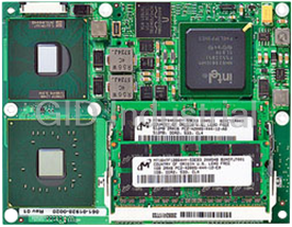


What they say about us
FANTASTIC RESOURCE
One of our top priorities is maintaining our business with precision, and we are constantly looking for affiliates that can help us achieve our goal. With the aid of GID Industrial, our obsolete product management has never been more efficient. They have been a great resource to our company, and have quickly become a go-to supplier on our list!
Bucher Emhart Glass
EXCELLENT SERVICE
With our strict fundamentals and high expectations, we were surprised when we came across GID Industrial and their competitive pricing. When we approached them with our issue, they were incredibly confident in being able to provide us with a seamless solution at the best price for us. GID Industrial quickly understood our needs and provided us with excellent service, as well as fully tested product to ensure what we received would be the right fit for our company.
Fuji
HARD TO FIND A BETTER PROVIDER
Our company provides services to aid in the manufacture of technological products, such as semiconductors and flat panel displays, and often searching for distributors of obsolete product we require can waste time and money. Finding GID Industrial proved to be a great asset to our company, with cost effective solutions and superior knowledge on all of their materials, it’d be hard to find a better provider of obsolete or hard to find products.
Applied Materials
CONSISTENTLY DELIVERS QUALITY SOLUTIONS
Over the years, the equipment used in our company becomes discontinued, but they’re still of great use to us and our customers. Once these products are no longer available through the manufacturer, finding a reliable, quick supplier is a necessity, and luckily for us, GID Industrial has provided the most trustworthy, quality solutions to our obsolete component needs.
Nidec Vamco
TERRIFIC RESOURCE
This company has been a terrific help to us (I work for Trican Well Service) in sourcing the Micron Ram Memory we needed for our Siemens computers. Great service! And great pricing! I know when the product is shipping and when it will arrive, all the way through the ordering process.
Trican Well Service
GO TO SOURCE
When I can't find an obsolete part, I first call GID and they'll come up with my parts every time. Great customer service and follow up as well. Scott emails me from time to time to touch base and see if we're having trouble finding something.....which is often with our 25 yr old equipment.
ConAgra Foods