Peak 650 User's Guide Rev. A October 2000
PEAK 650VL2B
Single Board Computer
User′′s Guide
′′
NEXCOM
Peak 650 User's Guide Rev. A October 2000
@Copyright 2000
All Rights Reserved
Manual edition 1, October 2000
The information in this document is subject to change without prior notice in order to improve reliability,
design and function and does not represent commitment on the part of the manufacturer.
In no event will the manufacturer be liable for direct, indirect, special, incidental, or consequential damages
arising out of the use or the possibility of such damages.
This document contains proprietary information protected by copyright. All rights are reserved. No part of
this manual may be reproduced by any mechanical, electronic, or other means in any form without prior
written permission of the manufacturer.
Trademarks
PEAK 650 is registered trademarks of NEXCOM Co., Ltd., IBM PC is a registered trademark of International
Business Machines Corporation. Intel and Pentium are registered trademarks of Intel Corporation. Award
is a registered trademark of Award Software, Inc. Other product names mentioned herein are used for
identification purposes only and may be trademarks and/or registered trademarks of their respective
companies.
NEXCOM
Peak 650 User's Guide Rev. A October 2000
How to use this guide
This manual is written to help you use Peak 650. It describes how to arrange various settings on the
Pentium CPU board to meet your requirements. It is briefed as follows:
Chapter 1, ntroduction”
gives an overview of the product specifications. It also tells you what are
included in the product package.
Chapter 2, witches and Connectors” describes the definitions and positions of Jumpers and Connectors
that you may easily configure and set up per your requirement.
Chapter 3, apability Expanding” describes how to change or expand the CPU Board by changing the
system memory and CPU to get more power out from the CPU board.
Chapter 4, ward BIOS Setup” describes how to use the advanced PCI/Green BIOS to control almost
every feature of the Peak 650.
The Appendix A describes how to set up the Watch Dog Timer (WDT) and gives an example to program the
WDT.
NEXCOM
Peak 650 User's Guide Rev. A October 2000
Contents
CHAPTER 1 INTRODUCTION ........................................................................................ 1-1
PECIFICATIONS
1-1 S .................................................................................................................................1-2
1-2 WHAT YOU'LL HAVE FROM THE PACKAGE .............................................................................................1-2
CHAPTER 2 SWITCHES AND CONNECTORS.............................................................. 2-1
2-1 MAIN BOARD LAYOUT.........................................................................................................................2-1
2-2 SWITCHES .........................................................................................................................................2-2
2-3 CONNECTORS ....................................................................................................................................2-3
CHAPTER 3 CAPABILITY EXPANDING......................................................................... 3-1
3-1 SYSTEM MEMORY ..............................................................................................................................3-1
3-2 CHANGE CPU....................................................................................................................................3-2
CHAPTER 4 AWARD BIOS SETUP................................................................................ 4-1
4-1 BIOS SETUP......................................................................................................................................4-1
Entering Setup.........................................................................................................................................4-1
Control Keys............................................................................................................................................4-2
Getting Help.............................................................................................................................................4-3
The Main Menu........................................................................................................................................4-4
Standard CMOS Features.......................................................................................................................4-6
Advanced BIOS Features Setup Menu ...................................................................................................4-9
Advanced Chipset Features Setup Menu..............................................................................................4-13
Integrated Peripherals...........................................................................................................................4-17
Power Management Setup....................................................................................................................4-21
PnP/PCI Configuration ..........................................................................................................................4-25
PC Health Status...................................................................................................................................4-27
Frequency/Voltage Control....................................................................................................................4-28
Supervisor/User Password Setting........................................................................................................4-29
Power-On Boot......................................................................................................................................4-30
4-2 BIOS REFERENCE -POST MESSAGE ..............................................................................................4-31
POST Beep ...........................................................................................................................................4-31
Error Messages.....................................................................................................................................4-31
4-3 BIOS REFERENCE -POST CODES ..................................................................................................4-35
APPENDIX ..................................................................................................................... 43
APPENDIXAWATCH DOG TIMER..............................................................................................................43
Watch Dog Timer Working Procedure .....................................................................................................43
Content
Peak 650 User's Guide Rev. A October 2000
Watch Dog Timer character and function.................................................................................................43
Watch Dog Timer Control Register ..........................................................................................................44
Watch Dog Timer Programming Procedure .............................................................................................45
�������������
Appendix B DVI Interface Pin Assignment ...
Appendix C CON1: Digital Video Signals Interface (12 bit)� ..���������
Content
Peak 650 User's Guide Rev. A October 2000
Chapter 1 Introduction
Welcome to the PEAK 650 the most powerful Intel 815E based single board computer.
NEXCOM’s PEAK 650 series combines the high performance and exceptional value of Intel Celeron /
Pentium III CPU and 815E chipset with a full-featured, new generation, full-size single board computer. The
Intel 815E chipset, which combining internal graphics, LAN, and support for 4 USB ports, Ultra DMA66/100
IDE interface, that meets the performance, stability and reliability requirements. Moreover, In order to meet
the network requirement, the PEAK 650 series add one more Ethernet Controller Intel 82559 to support dual
channel Ethernet.
For the Display solution, not only the Intel 82815 (GMCH) chipset integrated Graphics controller, PEAK 650
series also provide On Board Optional ATI Rage Mobility M4 3D VGA accelerator with on die 8MB or 16MB
memory to support 4X AGP, which is compatible with DVI specification to support LCD panel.
The Intel 82815 (GMCH) chipset integrated Graphics with Intel Dynamic Video Memory Technology , the
D.V.M.T. employs direct AGP and intelligent arbitration to dynamically allocate and de-allocate memory for
textures for applications requiring additional texture memory. The operating system requires allocation of up
to 1MB of system memory to support legacy VGA. System properties will display up to 1MB less than
physical system memory available to the operating system. The graphics driver for the Intel 815 configuration
will request up to 4MB of memory from the OS to implement a maximum 1024x768 screen resolution, 2MB
for a command buffer and 4MB used for Z-buffering. For high-end 3D applications, the drivers request
allocation of system memory from the O/S for AGP graphics textures. When the 3D application is closed, the
O/S will re-allocate system memory back for generic use.
With the on board NEXCOM proprietary PCI Interface, the optional EBK SCSI 2 module design with Adaptec
AIC-7890 Ultra 2 SCSI controller, and the module EBK SCSI 160D design with Adaptec AIC 7899 Dual Ultra
160 SCSI controller, giving the PEAK 650A a unique feature as a full function single board computer,
The board is suitable and valuable for all the embedded applications, which also well support with the
Windows 2000, Windows NT and Linux Operation system.
Introduction
1-1
Peak 650 User's Guide Rev. A October 2000
1-1 Specifications
Product Feature
! Intel Socket 370 Celeron/Pentium III CPU running at 66/100/133MHz FSB up to 1GHz.
! Support SDRAM up to 512MB (Max.), with 100/133MHz SDRAM interface. Non Register Module.
! Dual Channel Ethernet by Intel 82801 (ICH2) chipset integrated LAN controller and Intel 82559 Ethernet
Controller, support Alert-on-LAN.
! Intel 82815 (GMCH) chipset integrated Graphics controller.
! On Board Optional ATI Rage Mobility M4 3D VGA accelerator, support 4X AGP.
! ITE 8712 Enhanced Super I/O on board.
! On Board Nexcom proprietary PCI interface, Reserved 32bit PCI interface for EBK SCSI / EBK SCSI2 /
EBK SCSI 160D module (Optional)
! On Chip enhanced IDE x 2, support Ultra DMA/66/100.
! On Chip Two USB controllers double the bandwidth to 24Mbps across four ports.
! ACPI Function Support
! Hardware Monitor for system Voltage and Temperature.
! On Board Solid State Disk Socket for DiskOnChip up to 288MB, and reserved Power header beside
IDE connector to support DOM ( DiskOnModule )
! ISAMAX Support, Maximize ISA signals to support ISA Card up to 20
! Full-size SBC with PCI and ISA golden Finger
Specification
! System Architecture
!Full size SBC with PCI/ISA Golden finger
!Intel Socket 370 Celeron/Pentium III with 66/100/133MHz FSB
!PCI V2.1 complied
!PICMG 1.0 (Rev.2.0) complied
CPU Support
!
!Intel Brand New Socket 370 FC-PGA Celeron / Pentium III CPU with 128/256K cache on die,
running at 66/100/133MHz FSB up to 1GHz
!Support streaming SIMD instruction
! Main Memory
! Support SDRAM up to 512MB (Max.), without ECC and Non-Register Mode SDRAM
! 168 pin DIMM socket ×2
! Support 100/133MHz SDRAM interface
! Intel DVMT (Dynamic Video Memory Technology) offers a more efficient way to manage system
memory, enabling software drivers, working in concert with the intelligent arbiter and the operating
Introduction
1-2
Peak 650 User's Guide Rev. A October 2000
system, utilize all of the system memory to support richer graphics applications.
BIOS
!
!Award System BIOS
!Plug & Play support
!Advanced Power Management support
!Advanced Configuration & Power Interface support
!Jumperless for CPU FSB
!2M bits flash ROM, upgradeable to 4M bits
! Chip Set
!Intel 815E chipsets
82815 × 1 Graphics and Memory Controller Hub (GMCH)
82801 × 1 I/O Controller Hub (ICH2)
82802 × 1 Firmware Hub (FWH)
!ITE 8888F × 1 PCI to ISA Bridge
! On Board VGA
!Intel 82815 (GMCH) chipset integrated with Graphics controller
!Hardware motion compensation assist for software MPEG/DVD decode
!15 pin CRT connector ×1
On Board optional VGA
!
! ATI Rage Mobility M4 3D VGA accelerator. 4X AGP
! Fully PC 98 and PC 99 Compliant.
! Integrated 8MB of SDR Memory, upgradeable to 16MB
! 15 pin CRT connector ×1, DVI interface connector ×1
On Board LAN
!
!Dual channel Ethernet support
!Intel 82801 (ICH2) chipset integrated LAN controller
!Intel 82559 Single Ethernet controller
!Alert-on-LAN by Intel 82801 ( ICH2)
!10 Base T/100 Base TX support, full duplex
!Complied with PCI V2.1, IEEE802.3, IEEE 802.3U
!Drivers support�DOS/Windows, Windows 95/98/2000, Windows NT4.0, Netware, SCO Open Server
5.0, Linux.
!RJ45 connector ×2
Introduction
1-3
Peak 650 User's Guide Rev. A October 2000
! On Board Nexcom proprietary PCI interface
!Reserved 32bit PCI interface for EBK SCSI / EBK SCSI2 / EBK SCSI 160D module
On Board I/O
!
!ITE 8712 Enhanced Super I/O on board
!SIO×2, with 2x16C550 UARTs, 10 pin header ×2, Optional RS422/485 ×1 for COM2
!PIO×1, bi-directional, EPP/ECP support, 26 pin connector ×1
� �
!Floppy Disk controller�5.25 360KB/1.2MB, 3.5 720KB/1.2MB/1.44MB/2.88MB support, 34 pin
connector ×1
!On chip enhanced IDE x 2, PIO up to mode 4, DMA master up to mode 2, Ultra DMA/66/100 support,
40 pin connector × 2, total 4 E.IDE devices support
!On chip Keyboard, mouse controller, 5 pin connector x 1(for other keyboard)� 6 pin mini DIN
connector ×1, for PS/2 keyboard/mouse
!On board USB port ×4 (6pin header ×2)
!On Board buzzer ×1
2
!On board 2 pin header for I C
!On board 5 pin header for IrDA
!On Board 2 pin header for reset SW, 4 pin for speaker, 5 pin for keylock, 2 pin power SW
ACPI Function
!
!Soft Power off
!
Wake On LAN
!Wake On Keyboard
!Wake On Ring
!RTC alarm wake up
! On Board Solid State Disk Socket
!On board reserved socket for DOC of M-systems�2MB~288MB, etc
!Power header beside IDE connector to support DOM
! System Monitor
!Derived from Super IO ITE 8712 to support system monitor.
!7 voltage (For +3.3V, +5V, -5V , 5V STBY, +12V, −12V, and Vcore ×1)
!One Fan speed (For CPU)
!Two temperature
!Drivers support�Windows 95/98, Windows NT4.0/2000
! ISAMAX Support
!
Maximize ISA signals to support ISA cards up to 20
Watchdog Timer
!
Introduction
1-4
Peak 650 User's Guide Rev. A October 2000
�
!1,2,4 4 seconds time-out intervals
! Dimensions
!340mm(L) × 122mm(W)
! Power Requirements
!TBD for ( Max. Typical )
! Environments
!Operating temperatures�0°C to 60°C
!Storage temperatures�-20°C to 80°C
!Relative humidity�10% to 90% (Non-condensing)
! Certification
!CE Verification
!FCC Class A
! Model Available
! PEAK 650VL2 -- Full-size Socket 370 Celeron/Pentium III CPU card w/VGA/Dual LAN
! PEAK 650M8 –Full-size Socket 370 Celeron/Pentium III CPU card w/ATI M4 VGA w8MB /LANWhat
you'll have from the package
!
In addition to this manual, the PEAK 650 package includes the following items
Items 650VL2 650M8
PEAK 650 Board 1 1
Cable Set, include UDMA66 IDE Cable x 1; FDD
Cable x1 ; Internal Keyboard Connector x1 ; 11
COM and LPT Cable w/Bracket
Y CABLE PS/2 1 TO 2 KEYBOARD/MOUSE 1 1
ATX Power Cable connect SBC and BackPlane 1 1
Driver CD 1 1
PEAK 650 Quick Reference Guide Rev.A 1 1
If any of these items is missed or damaged, please contact your vendor for what you want
Introduction
1-5
Peak 650 User's Guide Rev. A October 2000
Chapter 2 Switches and Connectors
2-1 Main Board Layout
This chapter gives the definitions and shows where to locate the positions of switches and connectors.
2-1
Capability Expand
Peak 650 User's Guide Rev. A October 2000
2-2 Switches
Switches on the CPU board are used to select options for different functions used. The switch-on or off is
to accommodate the variations of the following table.
Switch Setting Table (*: default setup)
S1 (*: Default setting)
1 2 3 4 CPU FSB / Memory
ON ON OFF OFF * Auto detect
OFF OFF ON ON 66MHZ / PC100 SDRAM
OFF OFF OFF ON 100MHZ / PC100 SDRAM
OFF OFF ON OFF 133MHZ / PC133 SDRAM
OFF OFF OFF OFF Reserve
SW2 (*: Default setting)
SW2 1 234 5678910
RS232 (*) OFF OFF OFF ON OFF ON OFF OFF OFF OFF
RS422 ON ON ON OFF ON OFF ON ON ON ON
RS485 ON ON OFF ON ON OFF OFF OFF OFF ON
SW1 (*: Default setting)
SW1/M-System Disable (*) C0000 C8000 D0000 D8000
1 OFF ON ON ON ON
2 X ON ON OFF OFF
3X ON OFF ON OFF
4 X X XXX
2-2
Capability Expand
Peak 650 User's Guide Rev. A October 2000
2-3 Connectors
Jumper/Connector Define
J1: External speaker connector
Pin 1 Pin 2, 3 Pin4
Speaker signal GND VCC5
J2: Power supply type select:
Pin1-2 short AT power
Pin2-3 short ATX power
J4: 5VSB power cable connector
Pin 1 Pin 2 Pin3
5VSB GND ATX power supply S_ON”
Jp1: VCC5 power connector (for DOM)
Pin 1 Pin 2
VCC5 GND
Jp3: Keylock connector
Pin 1 Pin 3,5 Pin 4
VCC5 GND keylock signal
J13: Reset button
Pin 1-2 Reset
JP4: CMOS set up
Pin 1-2 Pin 2-3
Normal Clear CMOS
J9: Power On button (ATX)
Pin 1-2 Power on
J11: IDE LED connector
Pin 1 Pin 2
VCC5 IDE LED signal
2-3
Capability Expand
Peak 650 User's Guide Rev. A October 2000
IR1: IR connector
Pin 1 Pin 2 Pin 3 Pin 4 Pin 5
VCC5 NC IR_RX GND IR_TX
J12: External keyboard connector
Pin 1 Pin 2 Pin 3 Pin 4 Pin 5
Keyboard CLK Keyboard DAT NC GND5 VCC5
JP2: I2C connector
Pin 1 Pin2
SMB DAT SMB CLK
J17: NEXCOM Reserved
Note: For Model Peak 650VL and Peak 650M8, the Nexcom plug in Module EBK SCSI2 or EBK
SCSI160D cannot use Ad24 for IDSEL.
EBK SCSI 160D Jumper Setting
ON Board Active Terminal Resistor
Enable Disable
Channel A S1.1 OFF ON
Channel B S1.2 OFF ON
IDSEL Jumper
AD20 JP1.1, JP1.2 Short
AD24 JP1.2, JP1.3 Short
SCSI LED Jumper
Channel A LED+: JP2.1
LED-: JP2.2
Channel B LED+: JP2.3
LED-: JP2.4
2-4
Capability Expand
Peak 650 User's Guide Rev. A October 2000
Chapter 3 Capability Expanding
This chapter explains how you can expand capability of your CPU board in such aspects as system memory
and CPU.
3-1 System Memory
Peak650 support 2 slots for 168-pin 3.3V Non-registered DIMM modules, providing support for up to 512MB
of main memory using DIMM modules from 8MB to 256MB. The following is the example to install the
system SDRAM memory module combination.
Note:
1. It is highly recommended to use the PC-100 or PC-133 Specification DIMM module.
2. Due to limitation of Intel 815E chipset, the board can support the ECC memory module.
Module Size
Q y of Module DIMM1 DIMM2 Max. Size
1 1 st 8~256 MB 256 MB
2 1 st 2 nd 8~256 MB 512 MB
To insert the DIMMs, the modules must be oriented in
the correct way. Notice the notches of the DIMM.
Align these notches as shown in the diagram below.
Gently push the DIMM until the retainers on both
sides of the socket lock the module in place.
To remove a DIMM, push the retainers outwards to
release the module then pull the module out of the
socket.
3-1
Capability Expand
Peak 650 User's Guide Rev. A October 2000
3-2 Change CPU
To change the CPU, pull the handling bar of the socket upward to the other end to loosen the socket's
openings. Carefully lift the existing CPU up to remove it from the socket.
Removing CPU
Place the new CPU on the middle of the socket, orienting its beveled corner to line up with the socket's
beveled corner. Make sure the pins of the CPU fit evenly to the socket openings. Replace the handling
bar to fasten the CPU to the socket. Be sure to re-arrange the jumper setting for the correct external
clock.
Installing CPU
3-2
Capability Expand
Peak 650 User's Guide Rev. A October 2000
Chapter 4 AWARD BIOS Setup
Award's BIOS ROM has a built-in Setup program that allows users to modify the basic system configuration.
This type of information is stored in battery-backed RAM (CMOS RAM) so that it retains the Setup
information when the power is turned off.
4-1 BIOS Setup
Entering Setup
Power on the computer and press immediately will allow you to enter Setup. The other way to
enter Setup is to power on the computer, when the below message appears briefly at the bottom of the
screen during the POST (Power On Self Test), press key or simultaneously press , ,
and keys.
TO ENTER SETUP BEFORE BOOT
PRESS OR KEY
If the message disappears before you respond and you still wish to enter Setup, restart the system to try
again by turning it OFF then ON or pressing the "RESET" button on the system case. You may also
restart by simultaneously pressing , , and keys. If you do not press the keys at the
correct time and the system does not boot, an error message will be displayed and you will again be asked
to,
PRESS TO CONTINUE,
OR TO ENTER SETUP
4-1
BIOS Setup
Peak 650 User's Guide Rev. A October 2000
Control Keys
Up arrow Move to previous item
Down arrow Move to next item
Left arrow Move to the item in the left hand
Right arrow Move to the item in the right hand
Main Menu -- Quit and not save changes into CMOS
Esc key Status Page Setup Menu and Option Page Setup Menu -- Exit
current page and return to Main Menu
.
PgUp / �� key Increase the numeric value or make changes
/
�
PgDn / “− key Decrease the numeric value or make changes
/
General help, only for Status Page Setup Menu and Option Page
F1
F1 key
Setup Menu
Change color from total 16 colors. F2 to select color forward, (Shift)
(Shift)F2 key
F2 to select color backward
( )
F3 key Reserved
F4 key Reserved
Restore the previous CMOS value from CMOS, only for Option Page
F5 key
Setup Menu
Load the default CMOS value from BIOS default table, only for
F6 key
Option Page Setup Menu
F7 key Load the Setup default value, only for Option Page Setup Menu
F8 key Reserved
F9 key Reserved
F10 key Save all the CMOS changes, only for Main Menu
Table 4-1 Control Keys
4-2
BIOS Setup
Peak 650 User's Guide Rev. A October 2000
Getting Help
Main Menu
The on-line description of the highlighted setup function is displayed at the bottom of the screen.
Status Page Setup Menu/Option Page Setup Menu
Press to pop up a small help window that describes the appropriate keys to use and the possible
selections for the highlighted item. To exit the Help Window press or .
4-3
BIOS Setup
Peak 650 User's Guide Rev. A October 2000
The Main Menu
Once you enter Award BIOS CMOS Setup Utility, the Main Menu (Figure 1) will appear on the screen.
The Main Menu allows you to select from ten setup functions and two exit choices. Use arrow keys to
select among the items and press to accept or enter the sub-menu.
Standard CMOS Features
Use this menu for basic system configuration. See Page 4-6 for details.
Advanced BIOS Features
Use this menu to set the Advanced Features available on your system. See Page 4-9 for details.
Advanced Chipset features
Use this menu to change the values in the chipset registers and optimize your system's performance.
See Page 4-13 for details.
Integrated Peripherals
Use this menu to specify your settings for integrated peripherals. See Page 4-17 for details.
Power Management setup
Use this menu to specify your settings for power management See Page 4-21 for details.
4-4
BIOS Setup
Peak 650 User's Guide Rev. A October 2000
PnP/PCI Configuration
This entry appears if your system supports PnP / PCI Configuration. See Page 4-25 for details.
PC health Status
Display CPU/System Temperature, Fan speed and Voltages Value. See Page 4-27 for details.
Frequency/Voltage Control
Use this menu to specify your settings for frequency/voltage control. See Page 4-28 for details.
Load Fail-Safe Defaults
Use this menu to load the BIOS default values for the minimal/stable performance for your system to
operate.
Load Optimized Defaults
Use this menu to load the BIOS default values that are factory settings for optimal performance system
operations. While Award has designed the custom BIOS to maximize performance, the factory has the
right to change these defaults to meet their needs.
Set Supervisor/User Password
Change, set, or disable password of supervisor or user. It allows you to limit access to the system and
Setup, or just to Setup. See Page 4-29 for details.
Save & Exit Setup
Save CMOS value changes to CMOS and exit setup.
Exit Without Saving
Abandon all CMOS value changes and exit setup.
4-5
BIOS Setup
Peak 650 User's Guide Rev. A October 2000
Standard CMOS Features
The items in Standard CMOS Setup Menu are divided into 11 categories. Each category includes no,
one or more than one setup items. Use the arrow keys to highlight the item and then use the or
keys to select the value you want in each item.
Main Menu Selections
Item Options Description
Set the system date. Note that the eek
�
Date MMM DD YYYY day automatically changes when you set the
date
Time HH : MM : SS Set the system time
Options are in its sub menu
Press to enter the sub menu of
IDE Primary Master
detailed options
(Described in Table 4-3)
Options are in its sub menu
Press to enter the sub menu of
IDE Primary Slave
detailed options
(Described in Table 4-3)
IDE Secondary Options are in its sub menu
Press to enter the sub menu of
detailed options
Master (Described in Table 4-3)
IDE Secondary Options are in its sub menu
Press to enter the sub menu of
detailed options
Slave (Described in Table 4-3)
Select the type of floppy disk drive installed in
Drive A None
your system
4-6
BIOS Setup
Peak 650 User's Guide Rev. A October 2000
Drive B 360K, 5.25 in
1.2M, 5.25 in
720K, 3.5 in
1.44M, 3.5 in
2.88M, 3.5 in
3 Mode floppy disk drives (FDD) are 3 1/2”
drives used in Japanese computer systems.
Floppy 3 Mode Disabled, Drive A, Drive B,
If you need to access data stored in this kind
Both
of floppy, you must select this mode, and of
course you must have a 3 Mode floppy drive.
LCD
CRT
LCD&CRT Select the default video device
AUTO
LCD&CRT
All Errors
No Errors
Select the situation in which you want the
Halt On All, but Keyboard
BIOS to stop the POST process and notify you
All, but Diskette
All, but Disk/Key
Base Memory N/A Displays the amount of conventional memory
detected during boot up
Extended Memory N/A Displays the amount of extended memory
detected during boot up
Total Memory N/A Displays the total memory available in the
system
Table 4-2 Main Menu Selections
4-7
BIOS Setup
Peak 650 User's Guide Rev. A October 2000
IDE Adapters
The IDE adapters control the hard disk drive. Use a separate sub menu to configure each hard disk drive.
Use the legend keys to navigate through this menu and exit to the main menu. Use below table to
configure the hard disk.
Item Options Description
IDE HDD Auto- Press Enter Press Enter to auto-detect the HDD on this
detection channel. If detection is successful, it fills the
remaining fields on this menu.
�
IDE Primary Master None Selecting anual lets you set the remaining
fields on this screen. Selects the type of fixed
Auto
disk. "User Type" will let you select the
Manual
number of cylinders, heads, etc. Note:
PRECOMP=65535 means NONE !
Capacity Auto Display your disk drive Disk drive capacity (Approximated). Note that
size this size is usually slightly greater than the size
of a formatted disk given by a disk checking
program.
Access Mode Normal Choose the access mode for this hard disk
LBA
Large
Auto
����
The following options are selectable only if the DE Primary Master item is set to anual’
Cylinder Min = 0 Set the number of cylinders for this hard disk.
Max = 65535
Head Min = 0 Set the number of read/write heads
Max = 255
Precomp Min = 0 **** Warning: Setting a value of 65535 means
no hard disk
Max = 65535
Landing zone Min = 0 ****
Max = 65535
Sector Min = 0 Number of sectors per track
Max = 255
Table 4-3 Hard disk selections
4-8
BIOS Setup
Peak 650 User's Guide Rev. A October 2000
Advanced BIOS Features Setup Menu
This section allows you to configure your system for basic operation. You have the opportunity to select
the system default speed, boot-up sequence, keyboard operation, shadowing and security.
Virus Warning
Allows you to choose the VIRUS Warning feature for IDE Hard Disk boot sector protection. If this
function is enabled and someone attempt to write data into this area, BIOS will show a warning message
on screen and alarm beep.
Enabled Activates automatically when the system boots up causing a warning message to
appear when anything attempts to access the boot sector or hard disk partition table.
Disabled No warning message will appear when anything attempts to access the boot sector
or hard disk partition table.
! WARNING!
Disk boot sector is to be modified
Type "Y" to accept write or "N" to abort write
Award Software, Inc.
Note: This function is available only for DOS and other OSes that do not trap INT13.
4-9
BIOS Setup
Peak 650 User's Guide Rev. A October 2000
CPU Internal Cache/External Cache
These two categories speed up memory access. However, it depends on CPU/chipset design. The
�
default value is Enable. If your CPU without Internal Cache then this item PU Internal Cache will not
be show.
The Choice: Enabled/Disabled
CPU L2 Cache ECC Checking
This category could turn on the ECC of Pentium III L2 Cache or just disable it.
The Choice: Enabled/Disabled
Processor Number Feature
Intel included a serial number in their Pentium III processors as a unique system identifier. For privacy
reasons, you can disable this setting to prevent the release of this identifier.
The Choice: Enabled/Disabled
Quick Power On Self Test
This category speeds up Power On Self Test (POST) after you power on the computer. If it is set to
Enable, BIOS will shorten or skip some check items during POST.
The Choice: Enabled/Disabled
First / Second / Third Boot Device
The BIOS attempts to load the operating system from the devices in the sequence selected in these items.
The Choice: Floppy, LS/ZIP, HDD, SCSI, CDROM, Disabled.
Boot Other Device
Enabled
If all the selected boot devices failed to boot, select the BIOS will try to boot from the other boot
devices (in a predefined sequence) which are present but not selected as boot devices in the setup (and
Disabled
hence have not yet been tried for booting). If select , that may be present but not selected as boot
devices in setup.
Swap Floppy drive
If the system has two floppy drives, you can swap the logical drive name assignments.
The choice: Enabled/Disabled.
Boot Up Floppy Seek
Seeks disk drives during boot up. Disabling speeds boot up.
The Choice: Enabled/Disabled.
Boot Up NumLock Status
Select power on state for NumLock.
The Choice: Enabled/Disabled.
4-10
BIOS Setup
Peak 650 User's Guide Rev. A October 2000
Gate A20 Option
Select if chipset or keyboard controller should control GateA20.
Normal A pin in the keyboard controller controls GateA20
Fast Lets chipset control Gate A20
Typematic Rate Setting
Key strokes repeat at a rate determined by the keyboard controller. When enabled, the typematic rate
and typematic delay can be selected.
The Choice: Enabled/Disabled.
Typematic Rate (Chars/Sec)
Sets the number of times a second to repeat a key stroke when you hold the key down.
The Choice: 6, 8, 10, 12, 15, 20, 24, 30
Typematic Delay (Msec)
Sets the delay time after the key is held down before it begins to repeat the keystroke.
The Choice: 250, 500, 750, 1000.
Security Option
Select whether the password is required every time the system boots or only when you enter setup.
System The system will not boot and access to Setup will be denied if
the correct password is not entered at the prompt.
Setup The system will boot, but access to Setup will be denied if the
correct password is not entered at the prompt.
Note: To disable security, select PASSWORD SETTING at Main Menu and then you will be asked to enter
password. Do not type anything and just press , it will disable security. Once the security
is disabled, the system will boot and you can enter Setup freely.
MPS Version control For OS
This field specifies the version of MPS used by the motherboard.
The Choice: 1.1, 1.4
OS Select for DRAM > 64MB
Select the operating system that is running with greater than 64MB of RAM on the system.
The Choice: Non-OS2, OS2
4-11
BIOS Setup
Peak 650 User's Guide Rev. A October 2000
HDD S.M.A.R.T. Capability
S.M.A.R.T. (Self-Monitoring, Analysis and Reporting Technology) is a technology developed to manage
the reliability of the hard disk by predicting future device failures. The hard disk needs to be S.M.A.R.T.
capable. The settings for this option are Disabled or Enabled.
* Note: S.M.A.R.T. cannot predict all future device failures. S.M.A.R.T. should be used as a warning tool,
not as a tool to predict the device reliability.
The Choice: Enabled/Disabled.
4-12
BIOS Setup
Peak 650 User's Guide Rev. A October 2000
Advanced Chipset Features Setup Menu
Since the features in this section are related to the chipset in the CPU board and all are optimized, you are
not recommended to change the default settings in the setup table, unless you know very detailed of the
chipset features.
This section allows you to configure the system based on the specific features of the installed chipset.
This chipset manages bus speeds and access to system memory resources, such as DRAM and the
external cache. It also coordinates communications between the conventional ISA bus and the PCI bus.
It must be stated that these items should never need to be altered. The default settings have been
chosen because they provide the best operating conditions for your system. The only time you might
consider making any changes would be if you discovered that data was being lost while using your system.
The first chipset settings deal with CPU access to dynamic random access memory (DRAM). The default
timings have been carefully chosen and should only be altered if data is being lost. Such a scenario
might well occur if your system had mixed speed DRAM chips installed so that greater delays may be
required to preserve the integrity of the data held in the slower memory chips.
SDRAM CAS Latency Time
When synchronous DRAM is installed, the number of clock cycles of CAS latency depends on the DRAM
timing.
The Choice: 2, 3
4-13
BIOS Setup
Peak 650 User's Guide Rev. A October 2000
SDRAM Cycle Time Tras/Trc
Select the number of SCLKs for an access cycle.
The Choice: 5/7, 7/9.
SDRAM RAS-to-CAS Delay
This field let you insert a timing delay between the CAS and RAS strobe signals, used when DRAM is
written to, read from, or refreshed. Fast gives faster performance; and Slow gives more stable
performance. This field applies only when synchronous DRAM is installed in the system.
The Choice: 2, 3.
SDRAM RAS Precharge Time
If an insufficient number of cycles is allowed for the RAS to accumulate its charge before DRAM refresh,
the refresh may be incomplete and the DRAM may fail to retain data. Fast gives faster performance; and
Slow gives more stable performance. This field applies only when synchronous DRAM is installed in the
system.
The Choice: 2, 3.
System BIOS Cacheable
Selecting Enabled allows caching of the system BIOS ROM at F0000h-FFFFFh, resulting in better system
performance. However, if any program writes to this memory area, a system error may result.
The choice: Enabled, Disabled.
Video BIOS Cacheable
Select Enabled allows caching of the video BIOS, resulting in better system performance. However, if
any program writes to this memory area, a system error may result.
The Choice: Enabled, Disabled.
Memory Hole At 15M-16M
You can reserve this area of system memory for ISA adapter ROM. When this area is reserved, it cannot
be cached. The user information of peripherals that need to use this area of system memory usually
discusses their memory requirements.
The Choice: Enabled, Disabled.
CPU Latency Timer
�
When enabled this item, the CPU cycle will only be deferred after it has been held in a noop Stall for 31
clocks and another ADS# has arrived. When disabled, the CPU cycle will be deferred immediately after
the GMCH receives another ADS#.
The Choice: Enabled, Disabled.
4-14
BIOS Setup
Peak 650 User's Guide Rev. A October 2000
Delayed Transaction
The chipset has an embedded 32-bit posted write buffer to support delay transactions cycles. Select
Enabled to support compliance with PCI specification version 2.1.
The Choice: Enabled, Disabled
AGP Graphics Aperture Size
This field determines the effective size of the Graphic Aperture used for a particular GMCH configuration.
It can be updated by the GMCH-specific BIOS configuration sequence before the PCI standard bus
enumeration sequence takes place. If it is not updated then a default value will select an aperture of
maximum size.
The choice: 4, 8, 16, 32, 64, 128, 256
Display Cache Frequency
You can use this item to select the frequency of the display cache.
The Choice: 100MHZ, 133MHZ.
System Memory Frequency
You can use this item to select the operating frequency for the main system memory.
The Choice: Auto, 100MHZ, 133MHZ.
On-Chip Video Window Size
Select the on-chip video window size for VGA drives use.
The Choice: 32MB, 64MB, Disabled.
Onboard Display Cache Setting
Setting the onboard display cache timing.
CAS # Latency
Select the local memory clock periods.
The Choice: 2, 3
Paging Mode Control
Select the paging mode control.
The Choice: Close, Open.
RAS-to-CAS Override
Select the display cache clock periods control.
The Choice: Fast, Slow.
4-15
BIOS Setup
Peak 650 User's Guide Rev. A October 2000
RAS# Timing
This item controls RAS# active to Protegra, and refresh to RAS# active delay ( in local memory clocks).
The Choice: Fast, Slow.
RAS# Precharge Timing
This item controls RAS# precharge (in local memory clocks).
The choice: Fast, Slow.
4-16
BIOS Setup
Peak 650 User's Guide Rev. A October 2000
Integrated Peripherals
Onboard LAN2 H/W Active
This setting enables or disables the onboard LAN2.
The choice: Enabled, Disabled.
Onboard SCSI H/W Active
This setting enables or disables the onboard SCSI.
The choice: Enabled, Disabled.
Onboard LAN Boot ROM
Decide whether to invoke the boot ROM of the onboard LAN chip.
The choice: LAN1, LAN2, Disabled.
4-17
BIOS Setup
Peak 650 User's Guide Rev. A October 2000
Onboard SCSI Boot ROM
Decide whether to invoke the boot ROM of the onboard SCSI.
The choice: Enabled, Disabled.
On-Chip Primary/Secondary PCI IDE
The chipset contains a PCI IDE interface with support for two IDE channels. Select Enabled to activate the
primary/secondary IDE interface. Select Disabled to deactivate the primary/secondary IDE
The choice: Enabled, Disabled.
Note: 1. On-chip Secondary PCI IDE:
Enabled: enable secondary IDE port and BIOS will assign IRQ15 for this port.
Disabled: disable secondary IDE port and IRQ15 is available for other device. The item is optional
only for PCI BIOS.
2. Some of the sound cards have an onboard CD-ROM controller, which uses IDE Secondary Port.
�
In order to avoid PCI IDE conflict, the IDE secondary channel control has to select isabled then
CD-ROM can work.
IDE Primary/Secondary Master/Slave PIO
The four IDE PIO (Programmed Input/Output) fields let you set a PIO mode (0-4) for each of the four IDE
devices that the on-Board IDE interface supports. Modes 0 through 4 provide successively increased
performance. In Auto mode, the system automatically determines the best mode for each device.
The Choice: Auto, Mode 0, Mode 1, Mode 2, Mode 3 and Mode 4.
IDE Primary/Secondary Master/Slave UDMA
Ultra DMA/33 implementation is possible only if your IDE hard drive supports it and the operating
environment includes a DMA driver (Windows 95 OSR2 or a third-party IDE bus master driver). If your
hard drive and your system software both support Ultra DMA/33, select Auto to enable BIOS support.
The Choice: Auto, Disabled.
USB Controller
Select Enabled if your system contains a Universal Serial Bus (USB) controller and you have USB
peripherals.
The Choice: Enabled, Disabled.
USB Keyboard Support
Select Enabled if your system contains a Universal Serial Bus (USB) controller and you have a USB
keyboard.
The Choice: Enabled, Disabled.
4-18
BIOS Setup
Peak 650 User's Guide Rev. A October 2000
Init Display First
This item allows you to decide to active whether PCI Slot or on-chip VGA first
The Choice: PCI Slot, Onboard.
IDE HDD Block Mode
Block mode is also called block transfer, multiple commands, or multiple sector read/write. If your IDE
hard drive supports block mode (most new drives do), select Enabled for automatic detection of the
optimal number of block read/writes per sector the drive can support.
The Choice: Enabled, Disabled
Onboard FDC Controller
Select Enabled if your system has a floppy disk controller (FDC) installed on the system board and you
wish to use it. If you install add-on FDC Controller Card or the system has no floppy drive, select
Disabled in this field.
The Choice: Enabled, Disabled.
Onboard Serial Port 1/Port 2
Select an address and corresponding interrupt for the first and second serial ports.
The Choice: 3F8/IRQ4, 2E8/IRQ3, 3E8/IRQ4, 2F8/IRQ3, Disabled, Auto.
UART Mode Select
This item allows you to select UART mode.
The Choice: Normal, .IrDA, ASKIR
UR2 Duplex Mode
This item allows you to select the IR half/full duplex function.
The Choice: Half, Full.
Onboard Parallel Port
This item allows you to determine access On-Board parallel port controller with which I/O address.
The Choice: 3BC/IRQ7, 378/IRQ7, 278/IRQ5, Disabled.
Parallel Port Mode
Select an operating mode for the On-Board parallel (printer) port. Select Normal, Compatible, or SPP
unless you are certain your hardware and software both support one of the other available modes.
The Choice: SPP, EPP, ECP, ECP+EPP.
4-19
BIOS Setup
Peak 650 User's Guide Rev. A October 2000
ECP Mode Use DMA
Select a DMA channel for the parallel port for use during ECP mode.
The Choice: 3, 1.
4-20
BIOS Setup
Peak 650 User's Guide Rev. A October 2000
Power Management Setup
The Power Management Setup allows you to configure your system to most effectively save energy while
operating in a manner consistent with your own style of computer use.
ACPI Function
This item allows you to Enable/Disable the Advanced Configuration and Power Interface (ACPI).
The Choice: Enabled, Disabled.
ACPI Suspend Mode
This item will allow you to select the ACPI suspend type. You can select S3 (STR) for suspending to
DRAM or S1 (POS) for power on suspend under Windows 98 ACPI mode.
The choice: S1(POS), S3(STR).
4-21
BIOS Setup
Peak 650 User's Guide Rev. A October 2000
Power Management
This category allows you to select the type (or degree) of power saving and is directly related to the
following modes:
1. HDD Power Down
2. Doze Mode
3. Suspend Mode
There are four selections for Power Management, three of which have fixed mode settings.
Disabled (default) No power management. Disables all four modes
Min. Power Saving Minimum power management. Doze Mode = 1 hr. Standby Mode = 1 hr.,
Suspend Mode = 1 hr., and HDD Power Down = 15 min.
ONLY AVAILABLE FOR SL CPU
Max. Power Saving Maximum power management -- . Doze
Mode = 1 min., Standby Mode = 1 min., Suspend Mode = 1 min., and HDD
Power Down = 1 min.
User Define Allows you to set each mode individually. When not disabled, each of the
ranges are from 1 min. to 1 hr. except for HDD Power Down which ranges from
1 min. to 15 min. and Disabled.
Video Off Method
This determines the manner in which the monitor is blanked.
V/H SYNC+Blank This selection will cause the system to turn off the vertical and horizontal
synchronization ports and write blanks to the video buffer.
Blank Screen This option only writes blanks to the video buffer.
DPMS Initial display power management signaling.
Video Off In Suspend
This determines the manner in which the monitor is blanked.
The Choice: Yes, No.
Suspend Type
Select the Suspend Type.
The Choice: PWRON Suspend, Stop Grant.
MODEM Use IRQ
This determines the IRQ in which the MODEM can use.
The Choice: 3, 4, 5, 7, 9, 10, 11, NA.
4-22
BIOS Setup
Peak 650 User's Guide Rev. A October 2000
Suspend Mode
When enabled and after the set time of system inactivity, all devices except the CPU will be shut off.
The Choice: Enabled, Disabled.
HDD Power Down
When enabled and after the set time of system inactivity, the hard disk drive will be powered down while all
other devices remain active.
The Choice: Enabled, Disabled.
Soft-Off by PWR-BTTN
Pressing the power button for more than 4 seconds forces the system to enter the Soft-Off state when the
�
system has ung
The Choice: Delay 4 Sec, Instant-Off.
Wake-Up by PCI card
� �
When enabled, you can ake-up your system using a PCI rev2.2 card, when a ME# event occurring.
The Choice: Enabled, Disabled.
PowerOn by Ring
An input signal on the serial Ring Indicator (RI) line (in other words, an incoming call on the modem)
awakens the system from a soft off state.
The choice: Enabled, Disabled.
USB KB Wake-Up From S3
This item will enable you to wake-up the system by USB keyboard when you shut down the computer in S3
mode.
The choice: Enabled, Disabled.
Resume by Alarm
When Enabled, your can set the date and time at which the RTC (real-time clock) alarm awakens the
system from Suspend mode.
The choice: Enabled, Disabled.
4-23
BIOS Setup
Peak 650 User's Guide Rev. A October 2000
PM Events (Reload Global Timer Events)
PM events are I/O events whose occurrence can prevent the system from entering a power saving mode
or can awaken the system from such a mode. In effect, the system remains alert for anything which
occurs to a device which is configured as Enabled, even when the system is in a power down mode.
Primary IDE 0
Primary IDE 1
Secondary IDE 0
Secondary IDE 1
FDD, COM, LPT Port
PCI PIRQ[A-D] #
4-24
BIOS Setup
Peak 650 User's Guide Rev. A October 2000
PnP/PCI Configuration
P C I
This section describes configuring the PCI bus system. eripheral omponent nterface, is a system
which allows I/O devices to operate at speeds nearing the speed the CPU itself uses when communicating
with its own special components. This section covers some very technical items and it is strongly
recommended that only experienced users should make any changes to the default settings.
PNP OS Installed
Select Yes if the system operating environment is Plug-and-Play aware (e.g. Windows 95).
The Choice: Yes, No.
Reset Configuration Data
Normally, you leave this field Disabled. Select Enabled to reset Extended System Configuration Data
(ESCD) when you exit Setup if you have installed a new add-on Card and the system reconfiguration has
caused such a serious conflict that the operating system can not boot.
The choice: Enabled, Disabled .
4-25
BIOS Setup
Peak 650 User's Guide Rev. A October 2000
Resources Controlled by
The Award Plug and Play BIOS has the capacity to automatically configure all of the boot and Plug and
Play compatible devices. However, this capability means absolutely nothing unless you are using a Plug
�
and Play operating system such as Windows95. If you set this field to anual choose specific
resources by going into each of the sub menu that follows this field.
The Choice: Auto (ESCD), Manual.
M-System Memory Base
This function will be available when “Resources Controlled by” set to Manual
The Choice: N/A, C000, C800, D000, D800
IRQ/DMA Assigned To
This item allows you to determine the IRQ / DMA assigned to the ISA bus and is not available to any PCI
slot. (Legacy ISA) or PnP for both ISA and PCI.
Choices are Legacy ISA and PCI/ISA PnP.
Memory Resources
Used MEM Base Addr
Some add-in cards ask for a specific address space in the system memory. This field specifies the
memory base (start address) of the reserved memory space.
The Choice: N/A, C800, CC00, D000, D400, D800, DC00
Used MEM Length
This item is available only when the Used MEM Base Addr has been assigned a base address. It
specifies the memory size for the add-in card used.
The Choice: 8K, 16K, 32K, 64K
PCI/VGA Palette Snoop
Leave this field at Disabled.
The Choice: Enabled, Disabled.
Assign IRQ For VGA/USB
Enabled/Disable to assign a IRQ for VGA/USB.
The Choice: Enabled, Disabled.
4-26
BIOS Setup
Peak 650 User's Guide Rev. A October 2000
PC Health Status
Shutdown Temperature
This item allows you to set up the CPU shutdown Temperature. This item only effective under Windows
98 ACPI mode.
� � � �
The Choice: Disabled, 60 /140 , 65 /149 .
4-27
BIOS Setup
Peak 650 User's Guide Rev. A October 2000
Frequency/Voltage Control
Auto Detect DIMM/PCI Clk
When enabled, this item will auto detect if the DIMM and PCI socket have devices and will send clock
signal to DIMM and PCI devices. When disabled, it will send the clock signal to all DIMM and PCI socket.
The choice: Enabled, Disabled.
Spread Spectrum
This item allows you to enable/disable the spread spectrum modulate.
The choice: Enabled, Disabled.
CPU Host/PCI Clock/PC133
This item allows you to slightly adjust the clock frequency.
The choice: 66MHZ~166MHZ.
CPU Clock Ratio
This item allows you to set up the CPU clock ratio, but this function depends on different CPU performance.
It is only effective for those clock ratio haven been locked.
The choice: X3~X8
4-28
BIOS Setup
Peak 650 User's Guide Rev. A October 2000
Supervisor/User Password Setting
You can set either supervisor or user password, or both of then. The differences between are:
supervisor password : can enter and change the options of the setup menus.
user password : just can only enter but do not have the right to change the options of the setup
menus. When you select this function, the following message will appear at the
center of the screen to assist you in creating a password.
ENTER PASSWORD: ENTER PASSWORD: ENTER PASSWORD: ENTER PASSWORD:
Type the password, up to eight characters in length, and press . The password typed now will
clear any previously entered password from CMOS memory. You will be asked to confirm the password.
Type the password again and press . You may also press to abort the selection and not
enter a password.
To disable a password, just press when you are prompted to enter the password. A message
will confirm the password will be disabled. Once the password is disabled, the system will boot and you
can enter Setup freely.
PASSWORD DISABLED PASSWORD DISABLED PASSWORD DISABLED PASSWORD DISABLED
When a password has been enabled, you will be prompted to enter it every time you try to enter Setup.
This prevents an unauthorized person from changing any part of your system configuration.
Additionally, when a password is enabled, you can also require the BIOS to request a password every time
your system is rebooted. This would prevent unauthorized use of your computer.
You determine when the password is required within the BIOS Features Setup Menu and its Security
�
option (see Section 3). If the Security option is set to ystem the password will be required both at boot
�
and at entry to Setup. If set to etup prompting only occurs when trying to enter Setup.
4-29
BIOS Setup
Peak 650 User's Guide Rev. A October 2000
Power-On Boot
After you have made all the changes to CMOS values and the system cannot
boot with the CMOS values selected in Setup, restart the system by turning it
OFF then ON or Pressing the "RESET" button on the system case. You may
also restart by simultaneously press , , and keys.
Upon restart the system, immediately press to load BIOS default
CMOS value for boot up.
4-30
BIOS Setup
Peak 650 User's Guide Rev. A October 2000
4-2 BIOS Reference - POST Message
During the Power On Self Test (POST), if the BIOS detects an error requiring you to do something to fix, it
will either sound a beep code or display a message.
If a message is displayed, it will be accompanied by:
PR PR PR PRES ES ES ESSSSS <>>> TO CONT TO CONT TO CONT TO CONTINUE, INUE, INUE, INUE, <>- >>--< -<>- >>--< -<>O >> OR OR ORR <>>> TO ENTER SETUP TO ENTER SETUP TO ENTER SETUP TO ENTER SETUP
POST Beep
Currently there is only one beep code in BIOS. This code indicates that a video error has occurred and
the BIOS cannot initialize the video screen to display any additional information. This beep code consists
of a single long beep followed by two short beeps.
Error Messages
One or more of the following messages may be displayed if the BIOS detects an error during the POST.
This list includes messages for both the ISA and the EISA BIOS.
BIOS ROM checksum error-System halted.
The checksum of ROM address F0000H-FFFFFH is bad.
CMOS BATTERY HAS FAILED
CMOS battery is no longer functional. It should be replaced.
CMOS CHECKSUM ERROR
Checksum of CMOS is incorrect. This can indicate that CMOS has become corrupt. This error may
have been caused by a weak battery. Check the battery and replace if necessary.
DISK BOOT FAILURE, INSERT SYSTEM DISK AND PRESS ENTER
No boot device was found. This could mean that either a boot drive was not detected or the drive does
not contain proper system boot files. Insert a system disk into Drive A: and press . If you
assumed the system would boot from the hard drive, make sure the controller is inserted correctly and
all cables are properly attached. Also be sure the disk is formatted as a boot device. Then reboot the
system.
DISKETTE DRIVES OR TYPES MISMATCH ERROR - RUN SETUP
Type of diskette drive installed in the system is different from the CMOS definition. Run Setup to
reconfigure the drive type correctly.
DISPLAY SWITCH IS SET INCORRECTLY
Display switch on the motherboard can be set to either monochrome or color. This indicates the switch
is set to a different setting than indicated in Setup. Determine which setting is correct, and then
either turn off the system and change the jumper, or enter Setup and change the VIDEO selection.
4-31
BIOS Setup
Peak 650 User's Guide Rev. A October 2000
DISPLAY TYPE HAS CHANGED SINCE LAST BOOT
Since last powering off the system, the display adapter has been changed. You must configure the
system for the new display type.
EISA Configuration Checksum Error
PLEASE RUN EISA CONFIGURATION UTILITY
The EISA non-volatile RAM checksum is incorrect or cannot correctly read the EISA slot. This can
indicate either the EISA non-volatile memory has become corrupt or the slot has been configured
incorrectly. Also be sure the card is installed firmly in the slot.
EISA Configuration Is Not Complete
PLEASE RUN EISA CONFIGURATION UTILITY
The slot configuration information stored in the EISA non-volatile memory is incomplete.
Note: When either of these errors appear, the system will boot in ISA mode, which allows you to
run the EISA Configuration Utility.
ERROR ENCOUNTERED INITIALIZING HARD DRIVE
Hard drive cannot be initialized. Be sure the adapter is installed correctly and all cables are correctly
and firmly attached. Also be sure the correct hard drive type is selected in Setup.
ERROR INITIALIZING HARD DISK CONTROLLER
Cannot initialize controller. Make sure the cord is correctly and firmly installed in the bus. Be sure the
correct hard drive type is selected in Setup. Also check to see if any jumper needs to be set correctly
on the hard drive.
FLOPPY DISK CONTROLLER ERROR OR NO CONTROLLER PRESENT
Cannot find or initialize the floppy drive controller. Make sure the controller is installed correctly and
firmly. If there are no floppy drives installed, be sure the Diskette Drive selection in Setup is set to
NONE.
FLOPPY DISK(S) fail (80)
Unable to reset floppy subsystem.
FLOPPY DISK(S) fail (40)
Floppy Type mismatch.
Hard Disk(s) fail (80)
HDD reset failed
Hard Disk(s) fail (40)
HDD controller diagnostics failed.
Hard Disk(s) fail (20)
HDD initialization error.
Hard Disk(s) fail (10)
Unable to recalibrate Hard Disk.
4-32
BIOS Setup
Peak 650 User's Guide Rev. A October 2000
Hard Disk(s) fail (08)
Sector Verify failed.
Invalid EISA Configuration
PLEASE RUN EISA CONFIGURATION UTILITY
The non-volatile memory containing EISA configuration information was programmed incorrectly or has
become corrupt. Re-run EISA configuration utility to correctly program the memory.
NOTE: When this error appears, the system will boot in ISA mode, which allows you to run the
EISA Configuration Utility.
KEYBOARD ERROR OR NO KEYBOARD PRESENT
Cannot initialize the keyboard. Make sure the keyboard is attached correctly and no keys are being
pressed during the boot.
If you are purposely configurating the system without a keyboard, set the error halt condition in Setup to
� �
ALT ON item to LL BUT KEYBOARD This will cause the BIOS to ignore the missing keyboard
and continue the boot.
KEYBOARD IS LOCKED OUT-UNLOCK THE KEY
BIOS detect the keyboard is locked. P17 of keyboard controller is pulled low.
MANUFACTURING POST LOOP
System will repeat POST procedure infinitely while the P15 of keyboard controller is pulled low. This is
also used for M/B burn in test.
MEMORY ADDRESS ERROR AT ...
Indicates a memory address error at a specific location. You can use this location along with the
memory map for your system to find and replace the bad memory chips.
MEMORY TEST FAIL
BIOS reports the memory test fail if the On-Board memory is tested error.
MEMORY PARITY ERROR AT ...
Indicates a memory parity error at a specific location. You can use this location along with the memory
map for your system to find and replace the bad memory chips.
MEMORY SIZE HAS CHANGED SINCE LAST BOOT
Memory has been added or removed since the last boot. In EISA mode use Configuration Utility to
reconfigure the memory configuration. In ISA mode enter Setup and enter the new memory size in
the memory fields.
MEMORY VERIFY ERROR AT ...
Indicates an error verifying a value already written to memory. Use the location along with your
system's memory map to find and replace the bad memory chips
OFFENDING ADDRESS NOT FOUND
This message is used in conjunction with the I/O CHANNEL CHECK and RAM PARITY ERROR
messages when the Address that has caused the problem cannot be isolated.
4-33
BIOS Setup
Peak 650 User's Guide Rev. A October 2000
OFFENDING SEGMENT:
This message is used in conjunction with the I/O CHANNEL CHECK and RAM PARITY ERROR
messages when the segment that has caused the problem has been isolated.
PRESS A KEY TO REBOOT
This will be displayed at the bottom screen when an error occurs that requires you to reboot. Press any
key and the system will reboot.
PRESS F1 TO DISABLE NMI, F2 TO REBOOT
When BIOS detects a Non-maskable Interrupt condition during boot, this will allow you to disable the
NMI and continue to boot, or you can reboot the system with the NMI enabled.
RAM PARITY ERROR - CHECKING FOR SEGMENT ...
Indicates a parity error in Random Access Memory.
Should Be Empty But EISA Board Found
PLEASE RUN EISA CONFIGURATION UTILITY
A valid board ID was found in a slot that was configurated as having no board ID.
NOTE; When this error appears, the system will boot in ISA mode, which allows you to run the
EISA Configuration Utility.
Should Have EISA Board But Not Found
PLEASE RUN EISA CONFIGURATION UTILITY
The board installed is not responding to the ID request, or no board ID has been found in the indicated
slot.
NOTE: When this error appears, the system will boot in ISA mode, which allows you to run the
EISA Configuration Utility.
Slot Not Empty
Indicates that a slot designated as empty by the EISA Configuration Utility actually contains a board.
NOTE: When this error appears, the system will boot in ISA mode, which allows you to run the
EISA Configuration Utility.
SYSTEM HALTED, (CTRL-ALT-DEL) TO REBOOT ...
Indicates the present boot attempt has been aborted and the system must be rebooted. Press and
hold down the CTRL and ALT keys and press DEL.
Wrong Board In Slot
PLEASE RUN EISA CONFIGURATION UTILITY
The board ID does not match the ID stored in the EISA non-volatile memory.
NOTE: When this error appears, the system will boot in ISA mode, which allows you to run the
EISA Configuration Utility.
4-34
BIOS Setup
Peak 650 User's Guide Rev. A October 2000
4-3 BIOS Reference - POST Codes
POST (hex) Description
CFh Test CMOS R/W functionality.
C0h Early chipset initialization:
-Disable shadow RAM
-Disable L2 cache (socket 7 or below).
-Program basic chipset registers.
C1h Detect memory
-Auto-detection of DRAM size, type and ECC.
-Auto-detection of L2 cache (socket 7 or below).
C3h Expand compressed BIOS code to DRAM.
C5h Call chipset hook to copy BIOS back to E000h & F000h shadow RAM..
01h Expand the Xgroup codes locating in physical address 1000h:0.
02h Reserved.
03h Initial Superio_Early_Init switch.
04h Reserved.
05h 1. Blank out screen.
2. Clear CMOS error flag.
06h Reserved.
07h 1. Clear 8042 interface.
2. Initialize 8042 self-test.
08h 1. Test special keyboard controller for Winbond 977 series Super I/O chips.
2. Enable keyboard interface.
09h Reserved.
0Ah 1. Disable PS/2 mouse interface (optional).
2. Auto detect ports for keyboard & mouse followed by a port & interface swap (optional).
3. Reset keyboard for Winbond 977 series Super I/O chips.
0Bh Reserved
0Ch Reserved
0Dh Reserved
0Eh Test F000h segment shadow to see whether it is R/W-able or not. If test fails, keep beeping
the speaker.
0Fh Reserved
10h Auto detect flash type to load appropriate flash R/W codes into the run time area in F000
4-35
BIOS Setup
Peak 650 User's Guide Rev. A October 2000
POST (hex) Description
for ESCD & DMI support.
11h Reserved
12h Use walking 1 algorithm to check out interface in CMOS circuitry. Also set real-time
clock power status, and then check for override.
13h Reserved
14h Program chipset default values into chipset. Chipset default values are MODBINable by
OEM customers.
15h Reserved
16h Initial Early_Init_Onboard_Generator switch.
17h Reserved
18h Detect CPU information including brand, SMI type (Cyrix or Intel) and CPU level (586 or
686).
19h Reserved
1Ah Reserved
1Bh Initial interrupts vector table. If no special specified, all H/W interrupts are directed to
SPURIOUS_INT_HDLR & S/W interrupts to SPURIOUS_soft_HDLR.
1Ch Reserved
1Dh Initial EARLY_PM_INIT switch.
1Eh Reserved
1Fh Load keyboard matrix (notebook platform).
20h Reserved
21h HPM initialization (notebook platform).
22h Reserved
23h 1. Check validity of RTC value:
e.g. a value of 5Ah is an invalid value for RTC minute.
2. Load CMOS settings into BIOS stack. If CMOS checksum fails, use default value
instead.
3. Prepare BIOS resource map for PCI & PnP use. If ESCD is valid, take into consideration
of the ESCD legacy information.
4. Onboard clock generator initialization. Disable respective clock resource to empty PCI
& DIMM slots.
5. Early PCI initialization:
-Enumerate PCI bus number
-Assign memory & I/O resource
-Search for a valid VGA device & VGA BIOS, and put it into C000h:0.
4-36
BIOS Setup
Peak 650 User's Guide Rev. A October 2000
POST (hex) Description
24h Reserved
25h Reserved
26h Reserved
27h Initialize INT 09h buffer
28h Reserved
29h 1. Program CPU internal MTRR (P6 & PII) for 0-640KB memory address.
2. Initialize the APIC for Pentium class CPU.
3. Program early chipset according to CMOS setup. Example: On-Board IDE controller.
4. Measure CPU speed.
5. Invoke video BIOS.
2Ah Reserved.
2Bh Reserved.
2Ch Reserved.
2Dh 1. Initialize multi-language .
�
2. Put information on screen display, including Award title, CPU type, CPU speed
2Eh Reserved.
2Fh Reserved.
30h Reserved.
31h Reserved.
32h Reserved.
33h Reset keyboard except Winbond 977 series Super I/O chips.
34h Reserved.
35h Reserved.
36h Reserved.
37h Reserved.
38h Reserved.
39h Reserved.
3Ah Reserved.
3Bh Reserved.
3Ch Test 8254.
3Dh Reserved.
3Eh Test 8259 interrupt mask bits for channel 1.
3Fh Reserved.
4-37
BIOS Setup
Peak 650 User's Guide Rev. A October 2000
POST (hex) Description
40h Test 8259 interrupt mask bits for channel 2.
41h Reserved.
42h Reserved.
43h Test 8259 functionality.
44h Reserved.
45h Reserved.
46h Reserved.
47h Initialize EISA slot.
48h Reserved.
49h 1. Calculate total memory by testing the last double word of each 64KB page.
2. Program write allocation for AMD K5 CPU.
4Ah Reserved.
4Bh Reserved.
4Ch Reserved.
4Dh Reserved.
4Eh 1. Program MTRR of M1 CPU.
2. Initialize L2 cache for P6 class CPU & program CPU with proper cacheable range.
3. Initialize the APIC for P6 class CPU.
4. On MP platform, adjust the cacheable range to smaller one in case the cacheable
ranges between each CPU are not identical.
4Fh Reserved.
50h Initialize U.SB
51h Reserved.
52h Test all memory (clear all extended memory to 0).
53h Reserved.
54h Reserved.
55h Display number of processors (multi-processor platform).
56h Reserved.
57h 1. Display PnP logo.
2. Early ISA PnP initialization.
-Assign CSN to every ISA PnP device.
58h Reserved.
59h Initialize the combined Trend Anti-Virus code.
4-38
BIOS Setup
Peak 650 User's Guide Rev. A October 2000
POST (hex) Description
5Ah Reserved.
5Bh (Optional Feature).
Show message for entering AWDFLASH.EXE from FDD (optional).
5Ch Reserved.
5Dh 1. Initialize Init_Onboard_Super_IO switch.
2. Initialize Init_Onboard_AUDIO switch.
5Eh Reserved
5Fh Reserved
60h Okay to enter Setup utility; i.e. not until this POST stage users can enter the CMOS setup
utility.
61h Reserved.
62h Reserved.
63h Reserved.
64h Reserved.
65h Initialize PS/2 Mouse.
66h Reserved.
67h Prepare memory size information for function call:
INT 15h ax=E820h.
68h Reserved.
69h Turn on L2 cache.
6Ah Reserved.
6Bh Program chipset registers according to items described in Setup & Auto-configuration table.
6Ch Reserved.
6Dh 1. Assign resources to all ISA PnP devices.
2. Auto assign ports to onboard COM ports if the corresponding item in Setup is set to
�
UTO
6Eh Reserved.
6Fh 1. Initialize Floppy controller.
2. Setup Floppy related fields in 40:hardware.
70h Reserved.
71h Reserved.
72h Reserved.
73h (Optional Feature).
4-39
BIOS Setup
Peak 650 User's Guide Rev. A October 2000
POST (hex) Description
Enter AWDFLASH.EXE if :
-AWDFLASH is found in Floppy Drive.
�
-LT+F2 is pressed.
74h Reserved.
�
75h Detect & install all IDE devices: HDD, LS120, ZIP, CDROM .
76h Reserved.
77h Detect Serial ports & Parallel ports.
78h Reserved.
79h Reserved.
7Ah Detect & install Co-processor.
7Bh Reserved.
7Ch Reserved.
7Dh Reserved.
7Eh Reserved.
7Fh 1. Switch back to text mode if full screen logo is supported.
-If errors occur, report errors & wait for keys.
�
-If no errors occur or 1 key is pressed to continue.
2. Clear EPA or customization logo.
80h Reserved.
81h Reserved.
E8POST.ASM starts
82h 1. Call chipset power management hook.
2. Recover the text fond used by EPA logo (not for full screen logo).
3. If password is set, ask for password.
83h Save all data in stack back to CMOS.
84h Initialize ISA PnP boot devices.
85h 1. USB final Initialization.
2. NET PC: Build SYSID structure.
3. Switch screen back to text mode.
4. Set up ACPI table at top of memory.
5. Invoke ISA adapter ROMs.
6. Assign IRQs to PCI devices.
7. Initialize APM.
4-40
BIOS Setup
Peak 650 User's Guide Rev. A October 2000
POST (hex) Description
8. Clear noise of IRQs.
86h Reserved.
87h Reserved.
88h Reserved.
89h Reserved.
90h Reserved.
91h Reserved.
92h Reserved.
93h Read HDD boot sector information for Trend Anti-Virus code.
94h 1. Enable L2 cache.
2. Program boot up speed.
3. Chipset final initialization.
4. Power management final initialization.
5. Clear screen & display summary table.
6. Program K6 write allocation.
7. Program P6 class write combining.
95h 1. Program daylight saving.
2. Update keyboard LED & typematic rate.
96h 1. Build MP table.
2. Build & Update ESCD.
3. Set CMOS century to 20h or 19h.
4. Load CMOS time into DOS timer tick.
5. Build MSIRQ routing table.
FFh Boot attempt (INT 19h).
4-41
BIOS Setup
Peak 650 User's Guide Rev. A October 2000
This page is intentionally left blank.
4-42
BIOS Setup
Peak 650 User's Guide Rev. A October 2000
Appendix
Appendix A Watch Dog Timer
Watch Dog Timer Working Procedure
The Watch Dog Timer (WDT) is the special hardware device. The WDT function is to monitor the
computer system whether work normally, otherwise, it will have some measures to fix up the system.
It contains a receivable SQW signal from RTC, and could set time and can clear the counter function.
When time is up, WDT can send Reset or NMI signal.
Operator has to write a value into WDT Configuration Register (Write the control value to the Configuration
Port), and clear WDT counter (read the Configuration Port).
Watch Dog Timer character and function
WDT Configuration port F2h Default at F2h
Watch Dog Timer Disabled 1. Default at Disabled
Enabled 2. Enabled for user′s programming
WDT Time out active for Reset Default at Reset
NMI
WDT Active Time 1 sec Default at 64 sec
2 sec
4 sec
8 sec
16 sec
32 sec
64 sec
Apendix
Peak 650 User's Guide Rev. A October 2000
Watch Dog Timer Control Register
The Watch Dog Timer Control Register is to control the WDT working mode. You can write the value to
WDT Configuration Port.
The following is the Control Register bit definition.
76 54 32 10
XX X
111 : N/A
110 : Select 1 second
101 : Select 2 second
100 : Select 4 second
011 : Select 8 second
010 : Select 16 second
001 : Select 32 second
000 : Select 64 second
1 : Enable Watch Dog Timer
0 : Disable Watch Dog Timer
1 : Select NMI
0 : Select Reset
Don care
Apendix
Peak 650 User's Guide Rev. A October 2000
Watch Dog Timer Programming Procedure
• • • • Power on or reset the system
The initial value of WDT Control Register (D4~D0) is zero, when power is on or reset the system. The
following means the initial value of WDT ( 00000000b ) :
Bit Value Mean
4 0 Select Reset
3 0 Disable Watch Dog Timer
2, 1, 0 0 0 0 Select 64 second
Initialize the SQW of RTC (set SQW output period=0.5 second)
• • • •
To initialize the SQW of RTC Component is to set the SQW signal which is output period=0.5 second.
It offers the basic frequency of the WDT counter.
The following is an example of initializing the SQW signal program in Intel 8086 assembly language.
; (G ; (G ; (G ; (Generate SQW enerate SQW enerate enerate SQW SQW = = = = 0.5 Sec.) 0.5 Sec.) 0.5 0.5 Sec.) Sec.)
MMoovv dx, 70h dx, 70h
Mo Movv dx, 70h dx, 70h
Mo MMo Moovvvv ax, 0Ah ax, 0Ah ax, 0Ah ax, 0Ah
Ou OOu Ouutttt dx, al dx, dx, al dx, al al ; Out port ; Out port ; Out port ; Out port 70h = 0Ah 70h = 0Ah 70h = 0Ah 70h = 0Ah
Mo MMo Moovvvv dx, 71h dx, 71h dx, 71h dx, 71h
MMoovv ax, 2Fh ax, 2Fh
Mo Movv ax, 2Fh ax, 2Fh
Ou OOu Ouutttt dx, al dx, dx, al dx, al al ; Out port ; Out port ; Out port ; Out port 71h = 2Fh 71h = 2Fh 71h = 2Fh 71h = 2Fh
; (enable ; (enable ; (enable ; (enable the SQW the SQW the SQW the SQW output) output) output) output)
MMoovv dx, 70h dx, 70h
Mo Movv dx, 70h dx, 70h
Mo MMo Moovvvv ax, 0Bh ax, 0Bh ax, 0Bh ax, 0Bh
Ou OOu Ouutttt dx, al dx, dx, al dx, al al ; Out port ; Out port ; Out port ; Out port 70h = 0Bh 70h = 0Bh 70h = 0Bh 70h = 0Bh
Mo MMo Moovvvv dx, 71h dx, 71h dx, 71h dx, 71h
MMoovv ax, 0Ah ax, 0Ah
Mo Movv ax, 0Ah ax, 0Ah
Ou OOu Ouutttt dx, al dx, dx, al dx, al al ; Out port ; Out port ; Out port ; Out port 71h = 0Ah 71h = 0Ah 71h = 0Ah 71h = 0Ah
Apendix
Peak 650 User's Guide Rev. A October 2000
Clear the WDT
• • • •
Repeatedly read WDT Configuration Port and the interval cannot be longer than the preset time,
otherwise, the WDT will generate NMI or Reset signal for the system.
The following is an example of clear the WDT program in Intel 8086 assembly language.
; ( ; ( ; ( ; ( Clear the Clear the Clear the Clear the WDT) WDT) WDT) WDT)
Mov Mov dx, F2h dx, F2h ; ; Setting the WDT Setting the WDT configuration port configuration port
Mov Mov dx, F2h dx, F2h ; ; Setting the WDT Setting the WDT configuration port configuration port
In In In In al, al, al, al, dx dx dx dx
Note: Before running WDT, you must clear the WDT. It means to make sure the initial value is zero
before enabling the WDT.
• • • • WDT Control Register (Write to WDT configuration port)
You can set the WDT Control Register to control the WDT working mode.
The initial value of the WDT Control Register is as the following.
; (Setting ; (Setting ; (Setting ; (Setting the WDT Control Register the WDT Control Register the WDT Control Register the WDT Control Register as AL) as AL) as AL) as AL)
Mo MMo Moovvvv al, 0h al, al, 0h al, 0h 0h ; ; ; ; Setti Setti Setti Setting initial value = 0 ng initial value = 0 ng initial value = 0 ng initial value = 0 for for for for the WDT Control Register the WDT Control Register the WDT Control Register the WDT Control Register
You must plan the option of following:
1. Select NMI or Reset: decide D4 value in F2h.
i.e. Setting D4 = 0, then it select Reset
AANNDD al, 11101111b al, 11101111b ; Select Reset ; Select Reset
AN ANDD al, 11101111b al, 11101111b ; Select Reset ; Select Reset
i.e. Setting D4 = 1, then it select NMI
OR OR OR OR aaaal, l, l, l, 00010000b ; 00010000b ; 00010000b ; 00010000b ; Select Select Select Select NMI NMI NMI NMI
2. Select the time-out intervals of WDT (decide the values of D2, D1, D0 in F2h).
Example: D2~D0 = 0, the time-out interval will be 64 sec.
AN AAN ANNDDDD al, 11111000b al, 11111000b al, 11111000b al, 11111000b ; Setting ; Setting ; Setting ; Setting the time the time the time the time----out interval out interval out interval out interval as as as as 64 sec. 64 sec. 64 sec. 64 sec.
3. Enabled or Disabled the WDT ( decide D3 value in F2h).
i.e. D3=0, Disabled the WDT
AN AAN ANNDDDD al, 11110111b al, 11110111b al, 11110111b al, 11110111b ; ; ; ; Disable the Disable the Disable the Disable the WDT WDT WDT WDT
i.e. D3=1, Enabled the WDT
OR OR OR OR al, 00001000b al, 00001000b al, 00001000b al, 00001000b ; ; ; ; Enable the Enable the Enable the Enable the WDT WDT WDT WDT
Apendix
Peak 650 User's Guide Rev. A October 2000
After finishing the above setting, you must be output for the Control Register value to the WDT
Configuration Port. Then WDT will start according to the above setting.
MO MMO MOOVVVV dx, F2h dx, F2h dx, F2h dx, F2h ; Setting W ; Setting W ; Setting W ; Setting WDT Configuration Port DT Configuration Port DT Configuration Port DT Configuration Port
OOUUTT dx, dx, al al ; Output the ; Output the Control Register Value Control Register Value
OU OUTT dx, al dx, al ; Output the ; Output the Control Register Value Control Register Value
You should build in a mechanism in the program to continue to read the WDT Configuration Port for
clearing WDT before the time out.
Apendix
Peak 650 User's Guide Rev. A October 2000
Appendix B : DVI Interface Pin Assignment ( for ATI Mobility M4 model only)
Apendix
Peak 650 User's Guide Rev. A October 2000
Appendix C: CON1 Digital Video Signals Interface (12 bit)
1 LTV DATA 0 2 Vcc 1.8
3 LTV DATA 1 4 Vcc 1.8
5 LTV DATA 2 6 Vcc 1.8
7 LTV DATA 3 8 Vcc 1.8
9 LTV DATA 4 10 GND
11 LTV DATA 5 12 GND
13 LTV DATA 6 14 GND
15 LTV DATA 7 16 GND
17 LTV DATA 8 18 GND
19 LTV DATA 9 20 Vcc 3
21 LTV DATA 10 22 Vcc 3
23 LTV DATA 11 24 Vcc 3
25 LTV HSYNC 26 Vcc 3
27 LTV VSYNC 28 Vcc 5
29 LTV BLANK# 30 Vcc 5
31 LTV CLKOUT [ 0 ] 32 Vcc 5
33 LTV CLKOUT [ 1 ] 34 GND
35 TV CLKIN / INT# 36 PCI_RST#
37 LTV DA 38 5VFTSDA
39 LTV CK 40 5VFTSCL
Apendix


 Manufacturers


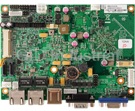
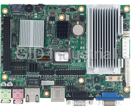
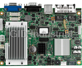
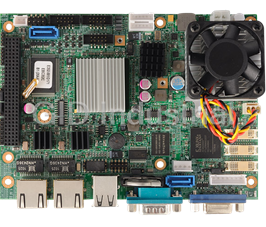
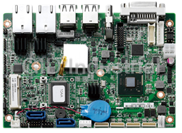


What they say about us
FANTASTIC RESOURCE
One of our top priorities is maintaining our business with precision, and we are constantly looking for affiliates that can help us achieve our goal. With the aid of GID Industrial, our obsolete product management has never been more efficient. They have been a great resource to our company, and have quickly become a go-to supplier on our list!
Bucher Emhart Glass
EXCELLENT SERVICE
With our strict fundamentals and high expectations, we were surprised when we came across GID Industrial and their competitive pricing. When we approached them with our issue, they were incredibly confident in being able to provide us with a seamless solution at the best price for us. GID Industrial quickly understood our needs and provided us with excellent service, as well as fully tested product to ensure what we received would be the right fit for our company.
Fuji
HARD TO FIND A BETTER PROVIDER
Our company provides services to aid in the manufacture of technological products, such as semiconductors and flat panel displays, and often searching for distributors of obsolete product we require can waste time and money. Finding GID Industrial proved to be a great asset to our company, with cost effective solutions and superior knowledge on all of their materials, it’d be hard to find a better provider of obsolete or hard to find products.
Applied Materials
CONSISTENTLY DELIVERS QUALITY SOLUTIONS
Over the years, the equipment used in our company becomes discontinued, but they’re still of great use to us and our customers. Once these products are no longer available through the manufacturer, finding a reliable, quick supplier is a necessity, and luckily for us, GID Industrial has provided the most trustworthy, quality solutions to our obsolete component needs.
Nidec Vamco
TERRIFIC RESOURCE
This company has been a terrific help to us (I work for Trican Well Service) in sourcing the Micron Ram Memory we needed for our Siemens computers. Great service! And great pricing! I know when the product is shipping and when it will arrive, all the way through the ordering process.
Trican Well Service
GO TO SOURCE
When I can't find an obsolete part, I first call GID and they'll come up with my parts every time. Great customer service and follow up as well. Scott emails me from time to time to touch base and see if we're having trouble finding something.....which is often with our 25 yr old equipment.
ConAgra Foods