

 Manufacturers
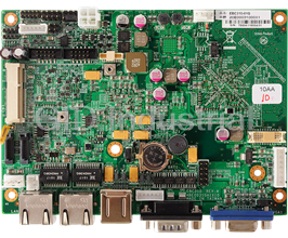
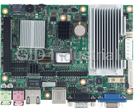
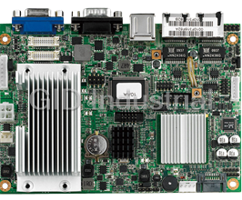
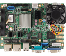
NEXCOM NEX852VL

Description
Micro-ATX Socket 478 Intel Pentium M/Celeron M processor, Marvell Gigabit LAN x 1
Part Number
NEX852VL
Price
Request Quote
Manufacturer
NEXCOM
Lead Time
Request Quote
Category
Single Board Computers
Specifications
System Chipset
Intel 852GM
Form Factor
Micro ATX
Micro-ATX 9.6" x 9.6"
?Relative humidity
10% to 90% non-condensing
?Storage Temperature Range
-20C to 80C
BIOS
Award System BIOS; ?ACPI Support; ?Advanced Power Management support; ?4M bits Flash ROM
Chipsets
Intel 852GM/GME with ICH4 I/O hub
CPU
Socket 478uFCPGA/479uFCBGA; Support Intel Pentium M: 2MB on Die L2 Cache, 400MHz FSB, speed up to 2.0GHz; Support Intel Pentium M:1MB on Die L2 Cache, 400MHz FSB, speed up to 1.7GHz; Support Intel Celeron M: 512KB on Die L2 Cache, 400MHz FSB, speed up to 1.5GHz
Expansion Slots
32-bit PCI slot x 4
Main Memory
184-pin DDR DIMM x 2; Support un-buffered non-ECC DDR 200/266 up to 1GB for NEX852VL
On-board LAN
Marvell GbE LAN 8001 x 2 (one is an option); RJ45 x 2 with LED
On-board VGA
Intel 852GME integrated dynamic video shared memory, 32MB max adjusted by OS; Resolution: Up to 1600 x 1200 for CRT or UP to 1280 x 1024 for TFT; D-sub 15-pin VGA port x 1; Internal LVDS: Support 18/24 bit single pixels or 18-bit dual pixels LVDS panel (Resolution support up to 1400 x 1050); ?Dual Display: Simultaneous Scan-CRT + LVDS LCD, Dual View-CRT + LVDS LCD
Operating Temperature Range
-20C to 60C
Processor
Intel Celeron M
Features
- ?184-pin DIMM x 2, support DDR 200/266 SDRAM memory up to 1GB
- ?Intel 852GM/GME chipset
- ?Internal Compact Flash socket X1 (optional)
- ?Serial Port x 2
- ?Support single/dual pixel LVDS panel display, CRT and LVDS dual display
- ?Support the Low Voltage/Ultra Low Voltage Intel Pentium M/Celeron M processors with 400MHz FSB
- ?USB 2.0 x 6
- Marvell Gigabit LAN x 2
- Support Intel Pentium M/Celeron M processor with 400MHz FSB
Datasheet

Extracted Text
www.nexcom.com
TheDigitalInfrastructure
NEX852VL Series
User Manual
2004-03Edition
Preface
Copyright
This publication, including all photographs, illustrations and software, is protected under international
copyright laws, with all rights reserved. No part of this manual maybe reproduced, copied, translated or
transmitted in any form or by any means without the prior written consent from NEXCOM International
Co., Ltd.
Version 1.0
Copyright 2003
Disclaimer
The information in this document is subject to change without prior notice and does not represent commit-
ment from NEXCOM International Co., LTD. However, users may update their knowledge of any product
in use by constantly checking its manual posted on our website: http://www.nexcom.com. NEXCOM shall
not be liable for direct, indirect, special, incidental, or consequential damages arising out of the use of any
product, nor for any infringements upon the rights of third parties, which may result from such use. Any
implied warranties of merchantability of fitness for any particular purpose is also disclaimed.
Acknowledgements
The NEX852VL(2) is a trademark of NEXCOM international CO., LTD. All other product names mentioned
herein are registered trademarks of their respective owners.
Regulatory Compliance Statements
This section provides the FCC compliance statement for Class A devices and describes how to keep the
system CE compliant.
FEDERAL COMMUNICATIONS COMMISSION (FCC) FOR CLASS A DEVICES
This equipment has been tested and verified to comply with the limits for a Class A digital device, pursu-
ant to Part 15 of FCC Rules. These limits are designed to provide reasonable protection against harmful
interference when the equipment is operated in a commercial environment. This equipment generates,
uses, and can radiate radio frequency energy and, if not installed and used in accordance with the
instructions, may cause harmful interference to radio communications. Operation of this equipment in a
residential area (domestic environment) is likely to cause harmful interference, in which case the user will
be required to correct the interference (take adequate measures) at their own expense.
CE CERTIFICATION
The product(s) described in this manual complies with all applicable European Union (CE) directives if it
has a CE marking. For computer systems to remain CE compliant, only CE-compliant parts may be used.
Maintaining CE compliance also requires proper cable and cabling techniques.
1
WARNINGS
Read and adhere to all warnings, cautions, and notices in this guide and
the documentation supplied with the chassis, power supply, and accessory
modules. If the instructions for the chassis and power supply are inconsis-
tent with these instructions or the instructions for accessory modules, con-
tact the supplier to find out how you can ensure that your computer meets
safety and regulatory requirements.
CAUTION
Electrostatic discharge (ESD) can damage NEX components. Do the de-
scribed procedures only at an ESD workstation. If no such station is available,
you can provide some ESD protection by wearing an antistatic wrist strap
and attaching it to a metal part of the computer chassis.
Safety Information
Before installing and using the NEX852VL(2), note the following precautions:
Read all instructions carefully.
Do not place the unit on an unstable surface, cart, or stand.
Follow all warnings and cautions in this manual.
When replacing parts, ensure that your service technician uses parts specified by the manufacturer.
Avoid using the system near water, in direct sunlight, or near a hearing device.
2
Table of Contents
Preface ...................................................................................................................................................1
Copyright ..................................................................................................................................................1
Disclaimer ................................................................................................................................................1
Acknowledgements .................................................................................................................................1
Regulatory Compliance Statements .......................................................................................................1
FEDERAL COMMUNICATIONS COMMISSION (FCC) FOR CLASS A DEVICES .................................1
CE CERTIFICATION ...............................................................................................................................1
WARNINGS ..................................................................................................................................2
CAUTION ......................................................................................................................................2
Safety Information .........................................................................................................................2
Table of Contents ...................................................................................................................... 3
Chapter 1 General Information ...............................................................................................5
1.1 Feature ..................................................................................................................................6
1.2 Specification ...........................................................................................................................6
1.3 Power Consumption Measurement.............................................................................................9
1.4 Board Layout .......................................................................................................................... 11
1.5 Board Dimensions ...................................................................................................................12
Chapter 2 Jumper Setting ......................................................................................................13
2.1 Before You Begin ...................................................................................................................14
2.2 Precautions ............................................................................................................................ 14
2.3 Setting Jumpers .....................................................................................................................15
2.4 Location of Jumpers ..............................................................................................................16
2.5 Function of Jumpers ..............................................................................................................16
2.6 Pin Definition..........................................................................................................................18
Chapter 3 Expansion Capability............................................................................................28
3.1 System Memory ..................................................................................................................... 29
3.2 Installing DIMM ......................................................................................................................30
3.3 Installing Compact Flash ........................................................................................................32
3.4 Installing Intel Pentium-M CPU and Fan Heatsink ......................................................................33
Chapter 4 Award BIOS Setup ..............................................................................................35
4.1 About the BIOS ......................................................................................................................36
4.2 When to Run BIOS ................................................................................................................36
4.3 Entering Setup ....................................................................................................................... 37
4.4 The Main Menu ......................................................................................................................37
4.5 Getting Help .......................................................................................................................... 38
4.6 Control Keys .......................................................................................................................... 39
4.7 Standard CMOS Features ......................................................................................................40
4.8 Advanced BIOS Features ........................................................................................................42
4.9 Advanced Chipset Features .....................................................................................................45
4.10 Integrated Peripherals ............................................................................................................47
4.11 Power Management Setup ....................................................................................................51
4.12 PnP/PCI Configurations .........................................................................................................53
3
4.13 PC Health Status ................................................................................................................54
4.14 Load Fail-Safe Defaults .........................................................................................................54
4.15 Load Optimized Defaults .......................................................................................................55
4.16 Set Password ......................................................................................................................55
4.17 Save & Exit Setup ................................................................................................................55
4.18 Exit Without Saving .............................................................................................................. 55
Appendix A Watchdog Timer ................................................................................................ 56
A.1 Watchdog Timer Working Procedure ....................................................................................... 57
A.2 Watchdog Timer Control Register ........................................................................................... 58
A.3 Watchdog Timer Programming Procedure ............................................................................... 58
Appendix B GPI/O Programming ..........................................................................................60
4
Chapter 1
General Information
5
1.1 Feature
® ® ®
* Support Intel Pentium M or Celeron M processor with 400MHz FSB
® ® ®
* Support the Low Voltage and Ultra Low Voltage Intel Pentium M or Intel Celeron M processor with
400MHz FSB
®
* Intel 852GM/GME
* 184-pin DIMM x 2 supports DDR 200/266/333 SDRAM memory up to 2GB
* Support single/dual pixel LVDS panel display
* CRT and LVDS dual display
* Single/dual Marvell Gigabit LAN
* Internal Compact Flash Socket x 1 (optional)
* Serial Ports x 2
* USB 2.0 x 6
1.2 Specifications
System Architecture
* Micro-ATX 9.6” x 9.6”
CPU Support
* Single 478uFCPGA/479uFCBGA socket
* Support Intel® Dothan: 2MB on die L2 cache with 400MHz FSB and speed up to 2.0GHz
* Support Intel® Pentium® M: 1MB on die L2 cache with 400MHz FSB and speed up to 1.7GHz
* Support Intel® Celeron® M: 512KB on die L2 cache with 400MHz FSB and speed up to 1.3GHz
Memory
* 184-pin DDR DIMM x 2
* Support unbuffered non-ECC DDR 200/266 up to 1GB for NEX852VL (Intel® 852GM)
* Support unbuffered ECC or non-ECC DDR 200/266/333 up to 2GB for NEX852VL2 (Intel®
852GME)
BIOS
* Award System BIOS
* ACPI Support
* Advanced Power Management support
6
* 4M bits flash ROM
Chipset
®
* Intel 852GM/GME with ICH4 I/O hub
LAN
* Marvell Gigabit LAN 8001 x 2 (one is optional)
* RJ45 x 2 with LED
Display
®
* Intel 852GME integrated dynamic video shared memory, 32MB(max.) adjusted by OS
* Resolution: up to 1600x1200 for CRT or up to 1280x1024 for TFT
* D-sub 15-pin VGA port x 1
* Internal LVDS: Support 18/24 bit single pixels or 18-bit dual pixels LVDS panel (Resolution support up
to 1400 x 1050)
* Dual Display: Simultaneous Scan-CRT + LVDS LCD, Dual View-CRT+LVDS LCD
I/O interface
* Serial Port x 2, with 16C550 UART x 2 (9-pin D-sub connector x 1, 10-pin header x 1)
* USB 2.0 x 6 (4 through Combo connector with RJ45, 2 from 6-pin header)
* HDD: 40-pin connector x 2, support ultra ATA 33/66/100 (Default: IDE channel 1)
* Optional Compact Flash Socket: Internal Compact Flash socket x 1 (Default: IDE Channel 2 master),
Type-II Compact Flash Card supported
* Parallel: 25-pin D-sub connector, bi-directional, EPP/ECP support
* Floppy: 34-pin connector x 1
* PS/2 Keyboard Mouse: 6-pin Mini-DIN connector x 1
* AC 97 audio: Phone Jack x 1 (Line-in /Line-out/Mic-in)
* On-board CD-in and Aux-in
* GPIO: 4 In and 4 Out
* IrDA: Onboard 5-pin header for IrDA Tx Rx
System Monitor
* Driver support for WIN2000, XP, XPe, Linux
* Monitoring of voltage, temperature and fans
* Watchdog Timer: Programmable via GAL by Software from 1-127 sec. or 1-127 min.
7
Expansion Slots
* 32-bit PCI slot x 4
Real-time Clock
* On-chip RTC with battery backup
* External Lithium Battery x 1
Watchdog Timer
* 1~127 seconds/minute time-out intervals
Dimensions
* 9.6” x 9.6” microATX compliant
Power Requirements
* Standard ATX 20-pin power connector
* Power consumption: measure with Intel® Dothan® 2.0GHz
a. +12V: 0.5A
b. +5V: 5.5A
c. +3.3V: 1A
d. +5Vsb: 0.1A
Environments
o o
* Operating temperatures: 0 C to 60 C
o o
* Storage temperatures -20 C to 80 C
* Relative humidity: 10% to 90% (Non-condensing)
Certification
* CE
* FCC A
Ordering Information
* NEX852VL: Micro-ATX Socket 478 Intel® Pentium® M/Celeron® M processor, Marvell Gigabit LAN x
1
* NEX852VL2: Micro-ATX Socket 478 Intel® Pentium® M/Celeron® M processor, Marvell Gigabit LAN
x 2 and CF socket
8
1.3 Power Consumption Measurement
NEX852VL2 Test Configuration:
Date In: 11/24/2004 Date Out: 11/24/2004
BIOS Version:C-002
Configuration Model Name
Pentium M/2.0GHz/Dothan
CPU Type/Speed/Model/Micro-Code
2.0G/(06D6/17D)
DDR/DDR333/512MB/SAMSUNG
Memory Type/Speed/Size/On-Board Chip/Vendor
K4H510838B-TCB3/UNIGEN
Power Supply Type/Model/Watts-Value ATX/Seventeam ST-250BLV/250W
LEMEL 5122
PS2 Keyboard and Mouse
Logitech M-BB48
HDD Drive HITACHI HDS722580VLAT20
CD-ROM Devices GIGABYTE GO-D1600B
Monitor Viewsonic P75f+
Windows 2000 Server
Operation System
(English)-5.00.2195+SP4
Test Software / Program HCT 9.5
NEX852VL Test Configuration:
In Date: 11/24/2004 Out Date: 11/24/2004
BIOS Version:C-002
Configuration Model Name
Pentium M/2.0GHz/Dothan
CPU Type/Speed/Model/Micro-Code
2.0G/(06D6/17D)
DDR/DDR333/512MB/SAMSUNG
Memory Type/Speed/Size/On-Board Chip/Vendor
K4H510838B-TCB3/UNIGEN
Power Supply Type/Model/Watts-Value ATX/Seventeam ST-250BLV/250W
LEMEL 5122
PS2 Keyboard and Mouse
Logitech M-BB48
HDD Drive HITACHI HDS722580VLAT20
CD-ROM Devices GIGABYTE GO-D1600B
Monitor Viewsonic P75f+
Windows 2000 Server
Operation System
(English)-5.00.2195+SP4
Test Software / Program HCT 9.5
9
Test Criteria:
1. Test configuration should include HDD drive and CD-ROM device.
2. Full loading mode should utilize CPU 100% with running of HCT test program.
Light loading mode will utilize CPU loading below 5%, and there is no data or application
running.
Test Result:
NEX852VL2(GME)
CPU Type: Dothan 2.0GHz
Low AC Line 110~115V: (System-Only)
+12V +5V +3.3V +5Vsb
Full-Loading Mode (A) 0.35 5.32 0.54 0.02
Light-Loading Mode (A) 0.34 2.77 0.54 0.02
Standby Mode (A) 0.28 2.07 0.53 0.01
Suspend to RAM (STR S4) (A) 0.06 0 0 0.39
NEX852VL(GM)
CPU Type: Dothan 2.0GHz
Low AC Line 110~115V: (System-Only)
+12V +5V +3.3V +5Vsb
Full-Loading Mode (A) 0.44 5.34 0.56 0.03
Light-Loading Mode (A) 0.44 2.71 0.56 0.02
Standby Mode (A) 0.38 2.09 0.55 0.02
Suspend to RAM (STR S4) (A) 0.01 0 0.03 0.35
10
1.4 Board Layout
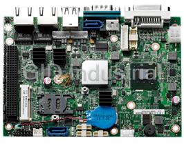
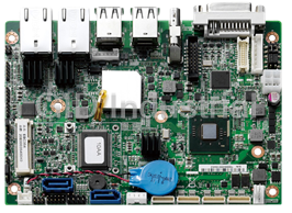
Figure 1.1 : Birdeye’s View of the NEX852
11
1.5 Board Dimensions
Figure 1.2 : Mechanical Drawing of the NEX852
12
Chapter 2
Jumper Setting
13
This chapter of the User Manual describes how to set jumpers.
Note: The procedures that follow are generic for all NEX852 models
2.1 Before You Begin
Ensure you have a stable, clean working environment. Dust and dirt can get into components and cause
a malfunction. Use containers to keep small components separated.
Adequate lighting and proper tools can prevent you from accidentally damaging the internal components.
Most of the procedures that follow require only a few simple tools, including the following:
A Phillips screwdriver
A flat-tipped screwdriver
A set of jewelers Screwdrivers
A grounding strap
An anti-static pad
Using your fingers can disconnect most of the connections. It is recommended that you do not use
needle-nosed pliers to disconnect connections as these can damage the soft metal or plastic parts of the
connectors.
Before working on internal components, make sure that the power is off. Ground yourself before touching
any internal components, by touching a metal object. Static electricity can damage many of the electronic
components. Humid environment tend to have less static electricity than dry environments. A grounding
strap is warranted whenever danger of static electricity exists.
2.2 Precautions
Computer components and electronic circuit boards can be damaged by discharges of static electricity.
Working on the computers that are still connected to a power supply can be extremely dangerous. Follow
the guidelines below to avoid damage to your computer or yourself:
Always disconnect the unit from the power outlet whenever you are working inside the case.
If possible, wear a grounded wrist strap when you are working inside the computer case. Alternatively,
discharge any static electricity by touching the bare metal chassis of the unit case, or the bare
metal body of any other grounded appliance.
Hold electronic circuit boards (such as the NEX852 board) by the edges only. Do not touch the
components on the board unless it is necessary to do so. Don’t flex or stress the circuit board.
Leave all components inside the static-proof packaging that they shipped with until they are ready
for installation.
Use correct screws and do not over tighten screws.
14
2.3 Setting Jumpers
A jumper is the simplest kind of electric switch. It consists of two metal pins and a cap. When setting the
jumpers, ensure that the jumper caps are placed on the correct pins. When the jumper cap is placed on
both pins, the jumper is SHORT. If you remove the jumper cap, or place the jumper cap on just one pin,
the jumper is OPEN. Please see the following illustrations
The illustrations on the right show
a 2-pin jumper. When the jumper
cap is placed on both pins, the
jumper is SHORT. If you remove
the jumper cap, or place the
jumper cap on just one pin, the
jumper is OPEN.
Open (Off) Short (On)
These illustrations show a 3-pin
jumper. Pins 1 and 2 are SHORT.
Table 2-1 : Setting Jumpers
15
2.4 Location of Jumpers
Figure 2-1: Jumper Location
2.5 Function of Jumpers
User can use jumpers to set configuration options. The table below defines function of each jumper:
Pin No. Function Pin No. Function
system speaker out, 4x1 pin LAN1 link/active LED, 2x1 pin
J1 J26
header header
CPLD programmer header, 6x1 LAN1 linking speed LED, 2x1
J2 J27
pin header pin header
GPIO port, 8 pin in/out, 6x2 pin
J3 J28 COM2, 5x2 pin box header
header
CRT out, HDS D-sub 15-pin
J4 aux in, 4x1 shrouded header J29
connector 1
LPT1 (parallel port), D-sub 25-
J5 CD in, 4x1 shrouded header J30
pin connector
To continue, please see the following page
16
Pin No. Function Pin No. Function
J6 system fan 1 connector J31 FDD, 17x2 box header
J7 system fan 2 connector J32 COM 1, D-sub 9-pin connector
J9 USB5/USB6, 5x2 pin header J33 SM-bus header
audio front I/O connector, 5x2
J10 J34 CPU fan connector
pin header
system power on LED/keyboard
J11 CF card socket J35
lock, 5x1 pin header
J12 panel backlight power connector J36 IrDA, 5x1 pin header
PS/2 keyboard/mouse, mini DIN
J13 heatsink holder J37
connector
CMOS setup clear, 3x1 pin
line in/headphone out/mic in, 3
J14 JP1 header (1-2 short for normal, 2-3
phone jack stackup connector
short for CMOS clear
panel digital power selection (1-2
J15 LVDS channel B connector JP2
short for 5V, 2-3 short for 3.3V)
CF card master/slave selection
J16 LVDS channel A connector JP3 jumper (short for master/NC for
slaves
CPU front side bus clock
LAN2 link/active LED, 2x1 pin
J17 JP5 100.133MHz (pin 1, 2 open
header
100MHz, Pin 1, 2 short 133MHz
LAN2+USB3/USB4, one port
ATX power connector, 10x2 pin
J18 RJ45+two port USB stackup CON1
heade
connector
LAN2 linking speed LED, 2x1
J19 PCI 1 PCI slot
pin header
ATX power on button, 2x1 pin
J20 PCI 2 PCI slot
header
J21 reset button, 2x1 pin header PCI 3 PCI slot
IDE access LED header, 2x1 pin
J22 PCI 4 PCI slot
header
LAN1+USB1/USB2, one port
J24 RJ45+two port USB stackup IDE 1 IDE channel 2, 20x2 pin header
connector
J25 heatsink holder IDE 2 IDE channel 1, 20x2 pin header
17
2.6 Pin Definition
J37: PS/2 Keyboard/Mouse mini DIN Connector
Keyboard:
Pin No. Description Pin No. Description
1 keyboard data 4 +5V
2 NC 5 keyboard clock
3 chassis ground 6 NC
PS/2 Mouse:
Pn inNo. D. escriptio Pn inNo Descriptio
1a m4 ouse dat +5V
2C N5 mouse clock
3d c6 hassis groun NC
J32: COM1, D-sub 9-pin Connector
Pn inNo. D. escriptio Pn inNo Descriptio
1) d6 ata carrier detect (DCD data set ready(DSR)
2) r7 eceive data (RXD request to send (RTS)
3) t8 ransmit data (TXD clear to send (CTS)
4) d9 ata terminalready(DTR ringindicator (RI)
5D GN
J29: CRT Out, HDS D-sub 15-pin Connector
Pn inNo. D. escriptio Pn inNo Descriptio
1d r9 e +5V
2n g0 ree 1d chassis groun
3e b1 lu 1C N
4C N2 1a DDC dat
5d c3 hassis groun 1c horizontalsyn
6d c4 hassis groun 1c verticalsyn
7d c5 hassis groun 1k DDC cloc
8d chassis groun
18
J24: LAN1+USB1/USB2, One Port RJ45+Two Ports USB Stackup Connector
LAN1
Pn inNo. D. escriptio Pn inNo Descriptio
1+ T5 X0 TX2-
2- T6 X0 TX1-
3+ T7 X1 TX3+
4+ T8 X2 TX3-
USB1/USB2
Pn inNo. Descriptio
1V +5
2- USB data
3+ USB data
4d Chassis Groun
J18: LAN2+USB3/USB4, One Port RJ45+Two Ports USB Stackup Connector
LAN 2
Pn inNo. D. escriptio Pn inNo Descriptio
1+ T5 X0 TX2-
2- T6 X0 TX1-
3+ T7 X1 TX3+
4+ T8 X2 TX3-
USB1/USB2
Pn inNo. Descriptio
1V +5
2- USB data
3+ USB data
4d Chassis Groun
J18: Line In/Headphone Out/Mic In, Three Phone Jacks Stackup Connector
Line In
Line Out
Microphone In
19
J36: IrDA, 5x1 Pin Header
Pn inNo. Descriptio
1V +5
2C N
3X IrR
4d groun
5X IrT
CON1:ATX Power Connector, 10x2 pin
Pn inNo. D. escriptio Pn inNo Descriptio
1V +1 3.3 1V +3.3
2V +2 3.3 1V -12
3d g3 roun 1d groun
4V +4 5 1n PS_o
5d g5 roun 1d groun
6V +6 5 1d groun
7d g7 roun 1d groun
8d p8 ower goo 1V -5
9B +9 5VS 1V +5
1V 0 +0 12 2V +5
J34/J6/J7: CPU Fan/System Fan1/System Fan2 Connector
Pn inNo. Descriptio
1d groun
2r programmable fanpowe
3r fanspeed senso
J28: COM2 5x2 Pin Box Header
Pn inNo. D. escriptio Pn inNo Descriptio
1D D2 C RXD
3D T4 X DTR
5d g6 roun DSR
7S R8 T CTS
9I R0 1C N
20
J30: LPT1 (Parallel Port), D-sub 25-pin Connector
Pn inNo. D. escriptio Pn inNo Descriptio
1e l4 ine printstrob 1d auto fee
20 p5 aralleldata 1r erro
31 p6 aralleldata 1e initializ
42 p7 aralleldata 1t selec
53 p8 aralleldata 1d groun
64 p9 aralleldata 1d groun
75 p0 aralleldata 2d groun
86 p1 aralleldata 2d groun
97 p2 aralleldata 2d groun
1e 0 a3 cknowledg 2d groun
1y 1 b4 us 2d groun
1y 2 p5 aper empt 2d groun
1t 3 s6 elec 2C N
J31: FDD, 17x2 Box Header
Pn inNo. D. escriptio Pn inNo Descriptio
1d g8 roun 1# DIR
2# D9 SNSEL 1d groun
3d g0 roun 2# STEP
4C N1 2d groun
5d g2 roun 2# WDATA
6C N3 2d groun
7d g4 roun 2# WGATE
8# I5 NDEX 2d groun
9d g6 roun 2# TK00
1# 0 M7 OTEA 2d groun
1d 1 g8 roun 2# WPT
1# 2 D9 RVB 2C N
1d 3 g0 roun 3# RDATA
1# 4 D1 RVA 3d groun
1d 5 g2 roun 3# side1
1# 6 M3 OTEB 3C N
1d 7 g4 roun 3# DSKCHG
21
J22: IDE Access LED Header, 2x1 Pin Header
Pn inNo. Descriptio
1+ LED
2- LED
IDE1/IDE2: IDE Channel 1/2, 20x2 Pin Header
Pn inNo. D. escriptio Pn inNo Descriptio
1# r2 eset ground
37 d4 ata data8
56 d6 ata data9
75 d8 ata data10
94 d0 ata 11 data1
13 1 d2 ata 12 data1
12 3 d4 ata 13 data1
11 5 d6 ata 14 data1
10 7 d8 ata 15 data1
1d 9 g0 roun 2C N
2Q 1 D2 MARE 2d groun
2# 3 I4 OW 2d groun
2# 5 I6 OR 2d groun
2Y 7 I8 OCHRD 2n pulldow
2# 9 D0 MAACK 3d groun
34 1 i2 nerrupt 1 3C N
31 3 d4 isk address 3t DMA66 Detec
30 5 d6 isk address 32 disk address
31 7 H8 DC CS 33 HDC CS
3D 9 H0 DDactive LE 4d groun
J3: GPIO Port, 8-pin In/Out, 6x2 Pin Header
Pn inNo. D. escriptio Pn inNo Descriptio
16 G2 PIO3 GPIO40
37 G4 PIO3 GPIO41
58 G6 PIO3 GPIO42
79 G8 PIO3 GPIO43
9v +0 5 1d groun
22
J5: CD In, 4x1 Shrouded Header
Pn inNo. Descriptio
1t CD inlef
2d CD groun
3d CD groun
4t CD inrigh
J4: Aux In, 4x1 Shrouded Header
Pn inNo. Descriptio
1t auxinlef
2d auxgroun
3d auxgroun
4t auxinrigh
J10: Audio Front I/O Connector, 5x2 Pin Header
Pn inNo. D. escriptio Pn inNo Descriptio
1- m6 ic line inright
2d g7 roun NC
3+ m8 ic key
4V +9 5 line out left
5t l0 ine out righ 1t line inlef
J9: USB5/USB6, 5x2 Pin Header
Pn inNo. D. escriptio Pn inNo Descriptio
1V +6 5 +5V
2- U7 SB5 USB6-
3+ U8 SB5 USB6+
4d g9 roun ground
5C N
J33: SM-Bus 2x1 Pin Header
Pn inNo. Descriptio
1a dat
2k cloc
23
J1: System Speaker Out, 4x1 Pin Header
Pn inNo. Descriptio
1- speaker
2d groun
3d groun
4+ speaker
J35: System Power on LED/Keyboard Lock, 5x1 Pin Header
Pn inNo. Descriptio
1+ LED
2C N
3- LED
4k keyloc
5d groun
J27: LAN1 Linking Speed LED, 2x1 Pin Header
Pn inNo. Descriptio
1 high 10M
2 high 10M
1
high 100M
2M low 100
1G low 1
2
high 1G
J26: LAN1 Link/Active LED 2x1 :Pin Header
Pn inNo. Descriptio
1+ LED
2- LED
J19: LAN2 Linking Speed LED 2x1 Pin Header
Pn inNo. Descriptio
1 high 10M
2
high 10M
1
high 100M
2M low 100
1G low 1
2
high 1G
24
J17: LAN2 Link/Active LED 2x1 Pin Header
Pn inNo. Descriptio
1+ LED
2- LED
J12: Panel Backlight Power Connector
Pn inNo. Descriptio
1V panelbacklight power +12
22 panelVDD(3.3V or 5V select byJP
3d groun
4d groun
5e panelbacklight enabl
6l panelbrightness contro
J16/J15: LVDS Channel A/B Connector
Pn inNo. D. escriptio Pn inNo Descriptio
1k p2 anelDDC cloc panelDDC data
panelVDD(3.3Vor 5V
3 40 LVDS_P
select byJP2)
53 L6 VDS_P LVDS_N0
panelVDD(3.3Vor
73 L8 VDS_N
5V select byJP2)
9d g0 roun 11 LVDS_YBP
1P 1 L2 VDS_CLKB 11 LVDS_YBN
1N 3 L4 VDS_CLKB 1d groun
panelbacklight power
1d 5 g6 roun 1
+12V
panelbacklight power
12 7 L8 VDS_P 1
+12V
12 9 L0 VDS_N 2d groun
25
J11: CF Card Socket
Pn inNo. D. escriptio Pn inNo Descriptio
1d g2 roun data3
34 d4 ata data5
56 d6 ata data7
71 H8 DC CS ground
9d g0 roun 1d groun
1d 1 g2 roun 1d groun
1V 3 +4 5 1d groun
1d 5 g6 roun 1d groun
1d 7 g8 roun 12 disk address
11 9 d0 isk address 20 disk address
20 1 d2 ata 21 data
22 3 d4 ata 2) IOCS16#(nc
2) 5 C6 F_cd2#(pull-down 2) CF_CD1#(pull-down
21 7 d8 ata1 22 data1
23 9 d0 ata1 34 data1
35 1 d2 ata1 33 HDC CS
3) 3 C4 F_VS1#(NC 3R IO
3W 5 I6 O 3) CF_WE#(+5V
35 7 i8 nterrupt 1 3V +5
CF_CSEL#(master or
39 4) 0 CF_VS2#(NC
slave)
4# 1 r2 eset 4Y IOCHRD
4) 3 D4 MAREQ/DACK(NC 4) DMAACK#/CF_REG#(+5V
4D 5 H6 DDActive LE 4# DMA66 detect/CF_PDIAG
48 7 d8 ata 49 data
40 9 d0 ata1 5d groun
26
PCI1/PCI2/PCI3/PCI4: PCI Slot
Pin Pin Pin Pin
Description Description Description Description
No. No. No. No.
A# 1 t2 est reset A6 3 A1 D1 BV -2 12 B7 3 AD1
CMD/byte enable2#
AV 2 +3 12 AV 3 +2 3.3 Bk t3 est cloc B3
Ae 3 t4 est mod A# 3 f3 rame Bd g4 roun Bd 3 groun
At 4 t5 est inpu Ad 3 g4 roun BC N5 B# 3 initiator ready
AV 5 +6 5 A# 3 t5 arget ready BV +6 5 BV 3 +3.3
A# 6 i7 nterruptA Ad 3 g6 roun BV +7 5 B# 3 device select
A# 7 i8 nterruptC A# 3 s7 top B# i8 nterruptB Bd 3 groun
AV 8 +9 5 AV 3 +8 3.3 B# i9 nterruptD B# 3 lock
AC 9 N0 AK 4 S9 M_CL BC N0 B# 4 parityerror
AV 10 +1 5 AA 4 S0 M_DAT BC 1 N1 BV 4 +3.3
AC 11 N2 Ad 4 g1 roun BC 1 N2 B# 4 systemerror
Ad 12 g3 roun Ay 4 p2 arit Bd 1 g3 roun BV 4 +3.3
CMD/byte enable1#
Ad 13 g4 roun A5 4 A3 D1 Bd 1 g4 roun B4
AX 14 35 .3VAU AV 4 +4 3.3 BC 1 N5 B4 4 AD1
A# 15 r6 eset A3 4 A5 D1 Bd 1 g6 roun Bd 4 groun
AV 16 +7 5 A1 4 A6 D1 Bk 1 c7 loc B2 4 AD1
A) 17 g8 rant(GNT# Ad 4 g7 roun Bd 1 g8 roun B0 4 AD1
Ad 18 g9 roun A9 4 A8 D B# 1 r9 equest Bd 4 groun
A# 19 P0 ME Ay 5 k9 eywa BV 1 +0 5 By 5 keywa
A0 20 A1 D3 Ay 5 k0 eywa B1 2 A1 D3 By 5 keywa
CMD/byte enable0#
AV 21 +2 3.3 A5 B9 21 A2 D2 B8 5 AD
A8 22 A3 D2 AV 5 +2 3.3 Bd 2 g3 roun B7 5 AD
A6 23 A4 D2 A6 5 A3 D B7 2 A4 D2 BV 5 +3.3
Ad 24 g5 roun A4 5 A4 D B5 2 A5 D2 B5 5 AD
A4 25 A6 D2 Ad 5 g5 roun BV 2 +6 3.3 B3 5 AD
At 26 I7 D selec A2 5 A6 D B2 CMD/byte enable3# Bd 57 groun
AV 27 +8 3.3 A0 5 A7 D B3 2 A8 D2 B1 5 AD
A2 28 A9 D2 AV 5 +8 5 Bd 2 g9 roun BV 5 +5
acknowledge 64bits#
A0 29 A0 D2 A# 6 r9 equest 64bits B1 2 A0 D2 B6
Ad 30 g1 roun AV 6 +0 5 B9 3 A1 D1 BV 6 +5
A8 31 A2 D1 AV 6 +1 5 BV 3 +2 3.3 BV 6 +5
27
Chapter 3
Expansion Capability
28
28
3.1 System Memory
Your system memory is provided by DIMM’s (Dual In-Line Memory Modules) on the CPU board. The
board contains two memory banks: Bank 0 and 1, which correspond to connector DIMM1 and DIMM2.
The table below shows possible DIMM Configurations for the memory banks. Please note that the NEX852VL2
supports Double Data Rate DDR 200/266/333 SDRAM. Configurations using different brands of memory
modules are not recommended.
D2 IMM1 Dl IMM Tota
1y 28 MB EB mpt 128 M
EB mpty 1B 28 M 128 M
1B 28 MB 1B 28 M 256 M
2y 56 MB EB mpt 256 M
EB mpty 2B 56 M 256 M
2B 56 MB 2B 56 M 512 M
5y 12 MB EB mpt 512 M
EB mpty 5B 12 M 512 M
5B 12 MB 5B 12 M 1024 M
1y 024 MB EB mpt 1024 M
EB mpty 1B 024 M 1024 M
1B 024 MB 1B 024 M 2048 M
Table 3-1: DIMM Configurations of the NEX852VL2
29
3.2 Installing DIMM
To install DIMM
1. Make sure the two handles of the DIMM sockets are in the “open” position, i.e. the handles stay
outward.
Figure3-1: How to Install DIMM (1)
2. Slowly slide the DIMM modules along the plastic guides in the both ends of the socket.
Figure 3-2: How to Install DIMM (2)
30
3. Then press the DIMM module down right into the socket, until a click is heard. That means the two
handles automatically locked the memory modules into the right position of the DIMM socket.
Figure 3-3: How to Install DIMM (3)
4. To take away the memory module, just push the both handles outward, the memory module will be
ejected by the mechanism in the socket.
Figure 3-4: How to Install DIMM (4)
31
3.3 Installing Compact Flash
1. To install a Compact Flash memory card into NEX852VL2, align the notches on the card with the Com-
pact Flash socket in the NEX852VL2. Then firmly insert the card into the socket until it is completely
seated.
Figure 3-5: How to Install Compact Flash Memory (1)
2. To remove the Compact Flash memory card from NEX852VL2, pull out the memory card from the Com-
pact Flash socket.
Figure 3-6: How to Install Compact Flash Memory (2)
32
3.4 Installing Intel Pentium-M CPU and Fan Heatsink
The NEX852VL2 supports a full range of Intel® Pentium®-M processors. Below is the installation instruction:
Note: Prepare a slot type screwdriver before starting the installation process.
1. Be sure that the beveled corner of the CPU as shown in the picture is aligned with that of the socket.
Figure 3-7: How to Install CPU (1)
2. Screw it tight as shown in the picture.
Figure 3-8: How to Install CPU (2)
33
3. Tear off the protective membrane of one side of the thermal pad and stick it on the CPU, while the other
side of the thermal pad is stuck on the heatsink after tearing off the protective membrane.
Figure 3-9: How to Install CPU (3)
4. Insert the fan power connector onto J2 on the NEX852VL(2) embedded CPU board.
Figure 3-10: How to Install fan heatsink (1)
34
Chapter 4
Award BIOS Setup
35 35
This chapter explains how to use the BIOS Setup program for the NEX852VL2. The current BIOS setup
pictures in the chapter is for reference only, which may change by the BIOS modification in the future. Users
can download any major updated items or reversion from NEXCOM web site http://www.nexcom.com.tw. If
any unclear message occurs, please contact NEXCOM customer service representative for help or log onto
http://www.nexcom.com.tw/contact/contact.htm.
4.1 About the BIOS
The BIOS (Basic Input and Output System) Setup program is a menu driven utility that enables you to
make changes to the system configuration and tailor your system to suit your individual work needs. It is
a ROM-based configuration utility that displays the system’s configuration status and provides you with a
tool to set system parameters. These parameters are stored in non-volatile battery-backed-up CMOS
RAM that saves this information even when the power is turned off. When the system is turned back on,
the system is configured with the values found in CMOS.
With easy-to-use pull down menus, you can configure such items as:
Hard drives, diskette drives, and peripherals
Video display type and display options
Password protection from unauthorized use
Power management features
The settings made in the Setup program intimately affect how the computer performs. It is important,
therefore, first to try to understand all the Setup options, and second, to make settings appropriate for the
way you use the computer.
4.2 When to Run BIOS
This program should be executed under the following conditions:
When changing the system configuration
When a configuration error is detected by the system and you are prompted to make changes to
the Setup program
When resetting the system clock
When setting the CPU clock speed so that it automatically runs either fast or slow
When redefining the communication ports to prevent any conflicts
When making changes to the Power Management configuration
When changing the password or making other changes to the security setup
Normally, CMOS setup is needed when the system hardware is not consistent with the information con-
tained in the CMOS RAM, whenever the CMOS RAM has lost power, or the system features need to be
changed.
36
4.3 Entering Setup
When the system is powered on, the BIOS will enter the Power-On Self Test (POST) routines. These
routines perform various diagnostic checks; if an error is encountered, the error will be reported in one of
two different ways:
If the error occurs before the display device is initialized, a series of beeps will be transmitted.
If the error occurs after the display device is initialized, the screen will display the error message.
Powering on the computer and immediately pressing allows you to enter Setup. Another way to
enter Setup is to power on the computer and wait for the following message during the POST:
TO ENTER SETUP BEFORE BOOT
PRESS KEY
Press the key or press the
Frequently asked questions
How does Industrial Trading differ from its competitors?

Is there a warranty for the NEX852VL?
Which carrier will Industrial Trading use to ship my parts?
Can I buy parts from Industrial Trading if I am outside the USA?
Which payment methods does Industrial Trading accept?
Why buy from GID?

Quality
We are industry veterans who take pride in our work

Protection
Avoid the dangers of risky trading in the gray market

Access
Our network of suppliers is ready and at your disposal

Savings
Maintain legacy systems to prevent costly downtime

Speed
Time is of the essence, and we are respectful of yours
Related Products
Ultra Low power Embedded Board with Intel Atom E640 processor On-board DDR2 1GB memory, VGA/ LVDS, 1...
Low power Embedded Board with Intel Atom N270 processor and based on Intel 945GSE 3D graphics engi...
3.5" On-board Intel Atom N270 1.66GHz CPU with 24-bit LVDS/Gigabit LAN/CF, Low power Embedded Board...
Low power Embedded Board with Intel Atom Dual Core D525 processor support DDR3 SO-DIMM memory modul...
Low power embedded board with Intel Atom processor D2700 and based on Intel integrated graphics en...
Low power embedded board with Intel Atom processor D2700 and based on Intel integrated graphics en...
Request a Quote

The quote request has been received
Close

Facing challenges or have inquiries? Feel free to contact us!
Call Us +1-469-283-2440
What they say about us
FANTASTIC RESOURCE
One of our top priorities is maintaining our business with precision, and we are constantly looking for affiliates that can help us achieve our goal. With the aid of GID Industrial, our obsolete product management has never been more efficient. They have been a great resource to our company, and have quickly become a go-to supplier on our list!
Bucher Emhart Glass
EXCELLENT SERVICE
With our strict fundamentals and high expectations, we were surprised when we came across GID Industrial and their competitive pricing. When we approached them with our issue, they were incredibly confident in being able to provide us with a seamless solution at the best price for us. GID Industrial quickly understood our needs and provided us with excellent service, as well as fully tested product to ensure what we received would be the right fit for our company.
Fuji
HARD TO FIND A BETTER PROVIDER
Our company provides services to aid in the manufacture of technological products, such as semiconductors and flat panel displays, and often searching for distributors of obsolete product we require can waste time and money. Finding GID Industrial proved to be a great asset to our company, with cost effective solutions and superior knowledge on all of their materials, it’d be hard to find a better provider of obsolete or hard to find products.
Applied Materials
CONSISTENTLY DELIVERS QUALITY SOLUTIONS
Over the years, the equipment used in our company becomes discontinued, but they’re still of great use to us and our customers. Once these products are no longer available through the manufacturer, finding a reliable, quick supplier is a necessity, and luckily for us, GID Industrial has provided the most trustworthy, quality solutions to our obsolete component needs.
Nidec Vamco
TERRIFIC RESOURCE
This company has been a terrific help to us (I work for Trican Well Service) in sourcing the Micron Ram Memory we needed for our Siemens computers. Great service! And great pricing! I know when the product is shipping and when it will arrive, all the way through the ordering process.
Trican Well Service
GO TO SOURCE
When I can't find an obsolete part, I first call GID and they'll come up with my parts every time. Great customer service and follow up as well. Scott emails me from time to time to touch base and see if we're having trouble finding something.....which is often with our 25 yr old equipment.
ConAgra Foods