

 Manufacturers
INTEL FW82371EB
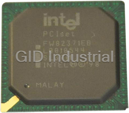
Description
Intel FW82371EB Embedded Processor - Embedded Processor 324-Pin BGA
Part Number
FW82371EB
Price
Request Quote
Manufacturer
INTEL
Lead Time
Request Quote
Category
Chipsets
Specifications
Notes
Engineering Sample (0.6 µ process)
Stepping
PIIX4E A-0
Datasheet

Extracted Text
R ® Intel 82371AB PIIX4, ® Intel 82371EB PIIX4E, ® Intel 82371MB PIIX4M Specification Update January 2002 ® ® ® Notice: The Intel 82371AB PIIX4, Intel 82371EB PIIX4E, and Intel 82371MB PIIX4M may contain design defects or errors known as errata which may cause the product to deviate from published specifications. Current characterized errata are documented in this Specification Update. Document Number: 297738-017 R ® Intel 82371AB PIIX4, 82371EB PIIX4E, 82371MB PIIX4M Information in this document is provided in connection with Intel® products. No license, express or implied, by estoppel or otherwise, to any intellectual property rights is granted by this document. Except as provided in Intel’s Terms and Conditions of Sale for such products, Intel assumes no liability whatsoever, and Intel disclaims any express or implied warranty, relating to sale and/or use of Intel products including liability or warranties relating to fitness for a particular purpose, merchantability, or infringement of any patent, copyright or other intellectual property right. Intel products are not intended for use in medical, life saving, or life sustaining applications. Intel may make changes to specifications and product descriptions at any time, without notice. Designers must not rely on the absence or characteristics of any features or instructions marked "reserved" or "undefined." Intel reserves these for future definition and shall have no responsibility whatsoever for conflicts or incompatibilities arising from future changes to them. ® ® ® The Intel 82371AB PIIX4, Intel 82371EB PIIX4E, and Intel 82371MB PIIX4M may contain design defects or errors known as errata which may cause the product to deviate from published specifications. Current characterized errata are available on request. Contact your local Intel sales office or your distributor to obtain the latest specifications and before placing your product order. Copies of documents which have an ordering number and are referenced in this document, or other Intel literature, may be obtained from: Intel Corporation www.intel.com or call 1-800-548-4725 Intel, Pentium and Xeon and the Intel logo are trademarks or registered trademarks of Intel Corporation or its subsidiaries in the United States or other countries. *Other names and brands may be claimed as the property of others. Copyright © 1997–2002, Intel Corporation 2 Specification Update R ® Intel 82371AB PIIX4, 82371EB PIIX4E, 82371MB PIIX4M Contents Revision History................................................................................................................... 4 Preface................................................................................................................................ 5 Specification Changes....................................................................................................... 13 Errata................................................................................................................................. 22 Specification Clarifications ................................................................................................ 35 Documentation Changes................................................................................................... 52 Specification Update 3 R ® Intel 82371AB PIIX4, 82371EB PIIX4E, 82371MB PIIX4M Revision History Rev. Draft/Changes Date -001 Initial Release Oct. 97 -002 Added PIIX4 Errata #11 Dec. 97 -003 Added Specification Change #2, Errata #12 and #13, and Documentation Change #6 Mar. 98 -004 Added Specification Change #3, Errata #14, Specification Clarifications #18 and #19, Apr. 98 Documentation Changes #7 and #8 -005 Added Errata #15 and Specification Clarification #20 Jun. 98 -006 Added Specification Change #4, Specification Clarifications #21-24 and Documentation Jul. 98 Change #9. -007 Added Errata #16 Aug. 98 -008 Added Specification Changes #5 - #7 Oct. 98 -009 Added Specification Change #8 and Errata #17–19 Feb. 99 -010 Added Specification Change #9 and Errata #20 Mar. 99 -011 Added Specification Change #10 and Errata #21 Apr. 99 -012 • Added Specification Changes #11-12, Errata #22, Specification Clarifications 25-26, and March 2001 Documentation Changes #10-12 • Added PIIX4E and PIIX4M specification update information. Added specification Changes #13-19 and Specification Clarification #27. These were previously in the PIIXE and/or PIIX4M Specification Updates and do not represent new information. -013 • Added current Specification Changes, Errata, Specification Clarifications and Document June 2001 Changes -014 • Added Specification Change #20 July 2001 -015 • Added October 2001 Specification Changes: Removal of SERIRQ Low Pulse Specification Specification Clarifications: PIORDY/SIORDY Minimum Deassertion Time -016 • Added November 2001 Errata: SE0 During Resume Causes Disconnect -017 • Added January 2002 Specification Change: ISA Signal Behavior During Reset 4 Specification Update R ® Intel 82371AB PIIX4, 82371EB PIIX4E, 82371MB PIIX4M Preface This document is an update to the specifications contained in the documents listed in the following Affected Documents/Related Documents table. It is a compilation of device and document errata and specification clarifications and changes, and is intended for hardware system manufacturers and for software developers of applications, operating system, and tools. Information types defined in the Nomenclature section of this document are consolidated into this update document and are no longer published in other documents. This document may also contain information that has not been previously published. This specification update is for the 82371AB PIIX4, 82371EB PIIX4E, and 82371MB PIIX4M components. Unless otherwise stated, the information in this document applies to all three components. Affected Documents/Related Documents Document Title Document Number ® Intel 82371AB PIIX4 datasheet 290562-001 Intel 82371AB (PIIX4) PCI ISA IDE Xcelerator Timing Specification 290548-001 Nomenclature Specification Changes are modifications to the current published specifications. These changes will be incorporated in the next release of the specifications. Errata are design defects or errors. Errata may cause the 82371AB PIIX4, 82371EB PIIX4E, and 82371MB PIIX4M, behavior to deviate from published specifications. Hardware and software designed to be used with any given stepping must assume that all errata documented for that stepping are present on all devices. Specification Clarifications describe a specification in greater detail or further highlight a specification’s impact to a complex design situation. These clarifications will be incorporated in the next release of the specifications. Documentation Changes include typos, errors, or omissions from the current published specifications. These changes will be incorporated in the next release of the specifications. Specification Update 5 R ® Intel 82371AB PIIX4, 82371EB PIIX4E, 82371MB PIIX4M Component Identification via Programming Interface ® The Intel 82371AB PIIX4, 82371EB PIIX4E, and 82371MB PIIX4M may be identified by the following register contents: 1 2 3 Stepping Vendor ID Device ID Revision Number 82371AB PIIX4 8086h 7110h See Documentation Changes section A-0, A-1, B-0 82371EB PIIX4E 8086h 7110h See Documentation Changes section A-0 82371MB PIIX4M 8086h 7110h See Documentation Changes section A-0 NOTES: 1. The Vendor ID corresponds to bits 15-0 of the Vendor ID Register located at offset 00-01h in the PCI function 0 configuration space. 2. The Device ID corresponds to bits 15-0 of the Device ID Register located at offset 02-03h in the PCI function 0 configuration space. 3. The Revision Number corresponds to bits 7-0 of the Revision ID Register located at offset 08h in the PCI function 0 configuration space. Component Marking Information The 82371AB PIIX4, 82371EB PIIX4E, and 82371MB PIIX4M may be identified by the following component markings: 82371AB PIIX4 Stepping S-Spec Top Marking Notes PIIX4 A-0 FW82371AB Q518ES Engineering Sample, FM Test PIIX4 A-0 FW82371AB Q519ES Engineering Sample, T3 Test PIIX4 A-1 FW82371AB Q532ES Engineering Sample, FM Test PIIX4 A-1 FW82371AB Q533ES Engineering Sample, T3, Burn in PIIX4 B-0 FW82371AB Q534ES Engineering Sample, FM Test PIIX4 B-0 FW82371AB Q535ES Engineering Sample, T3, Burn in PIIX4 B-0 SL23P FW82371AB SL23P Production PIIX4 B-0 SL2KM FW82371AB SL23P Production, Multiple FPO per Reel 6 Specification Update R ® Intel 82371AB PIIX4, 82371EB PIIX4E, 82371MB PIIX4M 82371EB PIIX4E Stepping S-Spec Top Marking Notes PIIX4E A-0 FW82371EB Q591ES Engineering Sample (0.6 µ process) PIIX4E A-0 FW82371EB Q592ES Engineering Sample (0.6 µ process) PIIX4E A-0 FW82371EB Q593ES Engineering Sample (0.6 µ process) PIIX4E A-0 FW82371EB Q594ES Engineering Sample (0.6 µ process) PIIX4E A-0 FW82371EB Q597ES Engineering Sample (0.6 µ process) PIIX4E A-0 FW82371EB Q598ES Engineering Sample (0.6 µ process) PIIX4E A-0 FW82371EB Q599ES Engineering Sample (0.6 µ process) PIIX4E A-0 FW82371EB Q600ES Engineering Sample (0.6 µ process) PIIX4E A-0 SL2MY FW82371EB SL2MY Production (0.6 µ process) PIIX4E A-0 SL2T3 FW82371EB SL2MY Production–Remnant lots (0.6 µ process) PIIX4E A-0 FW82371EB Q652ES Engineering Sample (0.35 µ process) PIIX4E A-0 FW82371EB Q653ES Engineering Sample (0.35 µ process) PIIX4E A-0 FW82371EB Q657ES Engineering Sample (0.35 µ process) PIIX4E A-0 SL37M FW82371EB SL37M Production (0.35 µ process) PIIX4E A-0 SL37U FW82371EB SL37M Production–Remnant lots (0.35 µ process) 82371MB PIIX4M Stepping S-Spec Top Marking Notes PIIX4M A-0 FW82371MB Q739ES Engineering Sample (0.35 µ process) PIIX4M A-0 FW82371MB Q740ES Engineering Sample (0.35 µ process) PIIX4M A-0 FW82371MB Q741ES Engineering Sample (0.35 µ process) PIIX4M A-0 SL3CG FW82371MB SL3CG Production (0.35 µ process) PIIX4M A-0 SL3DD FW82371MB SL3CG Production Remnant Spec (0.35 µ process) Specification Update 7 R ® Intel 82371AB PIIX4, 82371EB PIIX4E, 82371MB PIIX4M Summary Table of Changes The following table indicates the Specification Changes, Errata, Specification Clarifications or ® Documentation Changes, which apply to the listed Intel 82371AB PIIX4, 82371EB PIIX4E, and 82371MB PIIX4M steppings. Intel intends to fix some of the errata in a future stepping of the component and to account for the other outstanding issues through documentation or Specification Changes as noted. This table uses the following notations: Codes Used in Summary Table X: Erratum, Specification Change or Clarification that applies to this stepping. Doc: Document change or update that will be implemented. Fix: This erratum is intended to be fixed in a future stepping of the component. Fixed: This erratum has been previously fixed. NoFix There are no plans to fix this erratum. (No mark) or (Blank Box): This erratum is fixed in listed stepping or specification change does not apply to listed stepping. Shaded: This item is either new or modified from the previous version of the document. 8 Specification Update R ® Intel 82371AB PIIX4, 82371EB PIIX4E, 82371MB PIIX4M Number SPECIFICATION CHANGES 1 INTPN Register Not Implemented 2 Aliased NMI Enable Bit 3 IRQ9OUT# Is Active Level HI 4 CLKRUN# Re-Assertion 5 CNTB Granularity 6 CPU Stop Clock Exit Behavior 7 IDE Data Hold (t115b) Change 8 VCC Specification Change 9 INTLN Register Not Implemented 10 USB Host Controller Supports USB 1.1 11 Manufacturing ID at 0F8h (all Functions) May Vary 12 V /I for SMI# Changes to 10 mA @ 450 mV OL OL 13 Manual Throttle Duty Cycle (PIIX4E and PIIX4M only) 14 Enabling and Diabling Manual Throttling (PIIX4E and PIIX4M only) 15 RI# and USB Generate an SCI (PIIX4E and PIIX4M only) 16 Thermal Override Allows Break Events (PIIX4E and PIIX4M only) 17 Thermal Break Enable (PIIX4M only) 18 Throttle Period Change (PIIX4M only) 19 DC Spec Change for all CPU CMOS I/F Signals to 9.7mA @ 450mV (PIIX4E and PIIX4M only) 20 USB Clock PPM 21 Removal of SERIRQ Low Pulse Specification 22 ISA Signal Behavior During Reset Specification Update 9 R ® Intel 82371AB PIIX4, 82371EB PIIX4E, 82371MB PIIX4M NO. Steppings Plans ERRATA PIIX4 PIIX4E PIIX4M A0 A1 B0 A0 A0 1 X X X X X NoFix Burst Events May Cause LVL2 or LVL3 Register Reads to Be Missed 2 X X X X X NoFix PCI Accesses to External PCI-based IDE Devices will not cause Power Management Events 3 X X X X X NoFix General Purpose Outputs Default to Incorrect Values 4 X X X NoFix USB Bandwidth Reclamation 5 X X X Fix STPCLK# Deassertion Time 6 X X X X X NoFix Device Trap 7 X X X X X NoFix USB Rise / Fall Time Matching 8 X X X X X NoFix System Resume on USB OC# Assertion 9 X X X Fix PCI Arbiter Advances When PC/PCI ISA Master Gets Retried by the Host Controller 10 X X X X X NoFix Bus Master IDE Timeout 11 X X X X X NoFix USB-PCI Latency 12 X X X X X NoFix Device Monitor 9 and Access to IO Locations 62/66h 13 X X X X X NoFix USB Resume from Selective Suspend 14 X X X X X NoFix IRQ9OUT# Is Active HI 15 X X X X X NoFix IDE Prefetch 16 X X X X X NoFix SMI# Timing 17 X X X X X NoFix ISA Verify followed by PCPCI DMA 18 X X X X X NoFix C3 Power State/BMIDE & Type-F DMA Livelock 19 X X X X X NoFix USB Dribble 20 X X X X Fix ACPI Timer 21 X X X X X NoFix Daylight Savings Time 22 X X X X X NoFix USB Handshake 23 X X X X X NoFix SE0 During Resume Causes Disconnect 10 Specification Update R ® Intel 82371AB PIIX4, 82371EB PIIX4E, 82371MB PIIX4M Number SPECIFICATION CLARIFICATIONS 1 CONFIG[1] Definition 2 SUSA#, SUSB#, and SUSC# State Transition during Reset 3 IRQ8# Routing 4 IRQ9 Routing 5 SERIRQ Sample Phase 6 RI# Pulse Width Requirement 7 Diode Requirement for Vref Sequencing Circuit 8 SMI# Generation from APMC Write 9 Power Button Override 10 RTC Status Bit Clarification 11 SCI_EN Bit Clarification 12 Thermal Override Initiates Throttling Even in Clock Control State 13 No Disabling Break Events during a Burst 14 Unrouting a PIRQ 15 IDE Device Detection 16 Physical Region Descriptor Alignment 17 RTC Index Register Read 18 GPI[1] Minimum Assertion 19 RSMRST# Behavior 20 SM Bus Busy Bit Behavior 21 GPI14 for Device 5 Can Cause IO Trap SMI# 22 XDIR# Assertion 23 Correction to USB Bandwidth Reclamation Erratum Workaround 24 Do Not Use 4-Clock Serial IRQ Start Frame Width When CLKRUN# Is Enabled 25 SLP# Connectivity in Multi-Processor Systems 26 Serial IRQ Enable Clarification 27 Interrupt Deassertion (only 0.35 µ process device) (PIIX4E and PIIX4M only) 28 PIORDY/SIORDY Minimum Deassertion Time Specification Update 11 R ® Intel 82371AB PIIX4, 82371EB PIIX4E, 82371MB PIIX4M Number DOCUMENTATION CHANGES 1 PCI Revision ID Register Values 2 Interval Timer for IRQ0 3 Bus Master Activity for Burst Events 4 IRQ9 and IRQ9OUT# Pin Locations 5 PIO0 Timing Values ® ® 6 Sleep and Deep Sleep for Intel Pentium II Processors Only 7 SMI# Minimum Deassertion Time 8 Datasheet t37 Correction 9 Corrections to Simplified Block Diagram, Table 55, and Figure 34 10 Table 50 STD to ON Is Max Value 11 Fast_A20 12 INIT Assertion Correction 12 Specification Update R ® Intel 82371AB PIIX4, 82371EB PIIX4E, 82371MB PIIX4M Specification Changes 1. INTPN Register Not Implemented The PIIX4 datasheet, Section 7.1.9, INTPN—Interrupt Pin (Function 3), specified that the INTPN register indicates the PCI interrupt pin PIRQA# is used for routing Serial Interrupts. However, Serial Interrupts are hardwired to IRQ9. This register is not implemented. This change applies to all steppings of the PIIX4/PIIX4E/PIIX4M is planned to be incorporated into the next revision of the PIIX4 datasheet. 7.1.9 INTPN—INTERRUPT PIN (FUNCTION 3) Address Offset: 3Dh Default Value: 00h Attribute: Read only This register indicates that PCI interrupt pin PIRQA# is used for the Power Management module. Bit Description 7:0 Not Implemented 2. Aliased NMI Enable Bit The PIIX4 datasheet, Section 4.2.5.3, Real Time Clock Extended Index Register (IO), bit 7 description changes from Reserved to Aliased NMI Enable. This bit must always reflect the state of the NMI Enable bit, NMIEN[7] in IO space 70h. This change applies to all steppings of the PIIX4/PIIX4E/PIIX4M and is planned to be incorporated into the next revision of the PIIX4 datasheet. 3. IRQ9OUT# Is Active Level HI The PIIX4 datasheet and datasheet addendum, identify pin F3 (IRQ9OUT#/GPO29) as IRQ9OUT being active level LO in several places. When IRQ9OUT functionality is selected, the IRQ9OUT is active level HI, not active level LO. The name of this pin is changed to IRQ9OUT/GPO29. This change applies to all steppings of the PIIX4/PIIX4E/PIIX4M and is planned to be incorporated into the next revisions of the PIIX4 datasheet and datasheet addendum. Specification Update 13 R ® Intel 82371AB PIIX4, 82371EB PIIX4E, 82371MB PIIX4M 4. CLKRUN# Re-Assertion The PIIX4 datasheet on page 210, Section 11.2.3, PCI Clock Control, states if no other device in the system denies the request to stop before the fifth PCI clock, then the PIIX4 asserts the PCI_STP#. Any device must deny the request to stop before the fourth PCI clock. This change applies to all steppings of the PIIX4/PIIX4E/PIIX4M and is planned to be incorporated into the next revision of the PIIX4 datasheet. 5. CNTB Granularity The PIIX4 datasheet, Section 7.1.12, defines the Count B (Function 3) register functionality. CNTB[5] currently indicates that when this bit is set that the fast burst timer granularity is 1 µs. This is incorrect, the granularity, when CNTB[5] is set is 8 µs. This change applies to all steppings of the PIIX4/PIIX4E/PIIX4M and is planned to be incorporated into the next revision of the PIIX4 datasheet. 7.1.12 CNTB COUNT B (FUNCTION 3) Address Offset: 48-4Bh Default Value: 00h Attribute: Read/Write Bit Description 5 Processor PLL Lock Resolution (CPU_SEL) - R/W. Selects the clock resolution used for the fast burst timer when it is used to count the processor’s PLL lock time. 0= 1 ms granularity. 1= 8 µs granularity. 6. CPU Stop Clock Exit Behavior The PIIX4 datasheet, Section 11.2.2, Stop Clock and Deep Sleep State Example Sequence, page 209, describes the behavior when the processor is leaving the STOP CLOCK STATE. The first sentence in the third and fourth bullets are incorrect. The phrase “PIIX4 waits for the processor PLL to start and lock (about 1 ms + 32 kHz period) then negates the SUS_STAT1# signal {4}.” Is inaccurate. This sentence will be replaced by “PIIX4 waits for the processor PLL to start and lock (about CPU_LCK time + 32 kHz period) then negates the SUS_STAT1# signal {4}.” The sentence “PIIX4 waits up to 2-32 kHz periods and then negates the STPCLK# signal {5}.” Is inaccurate. This sentence will be replaced by “PIIX4 waits two–three 32 kHz periods (if SLEEP_EN=0), or three–five 32 kHz periods (if SLEEP_EN=1) and then negates the STPCLK# signal {5}.” This change applies to all steppings of the PIIX4/PIIX4E/PIIX4M and is planned to be incorporated into the next revision of the PIIX4 datasheet. 14 Specification Update R ® Intel 82371AB PIIX4, 82371EB PIIX4E, 82371MB PIIX4M 7. IDE Data Hold (t115b) Change Table 8 (PCI BUS IDE Timings), of the 82371AB (PIIX4) PCI ISA IDE Xcelerator Timing Specification datasheet addendum, defines t115b as an 8 ns min specification. This is specification is changed to 7 ns min to meet ATA Specification data hold requirements. This change applies to all steppings of the PIIX4/PIIX4E/PIIX4M and is planned to be incorporated into the next revision of the PIIX4 datasheet addendum. 8. V Specification Change CC The 82371AB (PIIX4) PCI ISA IDE Xcelerator Timing Specification datasheet addendum identifies the V range as 3.3 V ± 0.3 V. This specification is changed to 3.3 V ± 5%. CC This change applies to all steppings of the PIIX4/PIIX4E/PIIX4M and is planned to be incorporated into the next revision of the PIIX4 datasheet. 9. INTLN Register Not Implemented The PIIX4 datasheet specified that the INTLN register contain interrupt information concerning the power management module. However, this register is not implemented and is RESERVED. This change applies to all steppings of the PIIX4/PIIX4E/PIIX4M and is planned to be incorporated into the next revision of the datasheets. 10. USB Host Controller Supports USB 1.1 The PIIX4 datasheet specifies that the USB Host Controller is USB supports the USB Revision 1.0 Specification. The USB Host Controller in the PIIX4 is USB Revision 1.1 compliant. This change applies to all steppings of the PIIX4/PIIX4E/PIIX4M and is planned to be incorporated into the next revision of the datasheet. 11. Manufacturing ID at 0F8h (All Functions) May Vary A manufacturing ID field (0F8h) of PIIX4E functions 0–3 may return a value of 28h or 30h. This register is a RESERVED REGISTER and should not be accessed. This change applies to all steppings of the PIIX4E and is planned to be incorporated into the next revision of the PIIX4 datasheet. Specification Update 15 R ® Intel 82371AB PIIX4, 82371EB PIIX4E, 82371MB PIIX4M 12. V /I for SMI# Changes to 10 mA @ 450 mV OL OL The DC Characteristics for SMI#, as specified in the 82371AB (PIIX4) PCI ISA IDE Xcelerator Timing Specification datasheet addendum is changed from 7 mA @ 400 mV to 10mA @ 450 mV to accommodate stronger external pull-up resistors. 7:0 Not Implemented This change applies to all steppings of the PIIX4/PIIX4E/PIIX4M and is planned to be incorporated into the next revision of the 82371AB (PIIX4) PCI ISA IDE Xcelerator Timing Specification datasheet addendum. 13. Manual Throttle Duty Cycle (PIIX4E and PIIX4M only) The throttle duty cycle bits (THTL_DTY) in the Processor Control Register (PCNTRL) are being changed to match the ACPI specification. This change applies to all steppings of the PIIX4E and PIIX4M and is planned to be incorporated into the next revision of the datasheets. 7.2.7 PCNTRL —PROCESSOR CONTROL REGISTER (IO) I/O Address: Base + (10h) Default Value: 00h Attribute Read/Write Bit Description 3:1 Throttle Duty Programming Bits (THTL_DTY)—R/W. Selects the duty cycle of the STPCLK# signal when the system is in the system throttling mode. The duty cycle indicates the percentage of time the STPCLK# signal is asserted while in the throttle mode. The field is decoded as follows: Bits[2:0] Mode Bits[2:0] Mode 000 Reserved 100 50% 001 87.5% 101 37.5% 010 75% 110 25% 011 62.5% 111 12.5% 16 Specification Update R ® Intel 82371AB PIIX4, 82371EB PIIX4E, 82371MB PIIX4M 14. Enabling and Disabling Manual Throttling (PIIX4E and PIIX4M only) For the PIIX4, the manual throttling state is initiated by setting CC_EN, THT_EN and reading the LVL2 register. A break event will disable throttling and another LVL2 read is required to restart throttling. On the PIIX4E, break events will not disable manual throttling. Manual throttling mode begins when CC_EN and THT_EN are set. Manual throttling mode is disabled when either CC_EN or THT_EN is disabled. This change applies to all steppings of the PIIX4E and PIIX4M and is planned to be incorporated into the next version of the datasheets. 11.2.1 HOST CLOCK CONTROL MECHANISMS Table 1. Clock Programming Modes Clock Control Mode Register Read CC_EN STP_CLK_EN SLEEP_EN THT_EN Stop Grant/Quick LVL 2 1 X X 0 Start without Throttle Stop Grant/Quick None Required 1 X X 1 Start with Throttle Stop Grant/Quick LVL 2 1 X X 1 Start without Throttle, Throttling begins upon Stop Break Event System Throttle Control: If the system has been placed into the Stop Grant or Quick Start states and [THT_EN] bit is set, PIIX4 toggles the STPCLK# signal and ZZ signal (If [ZZ_EN] set) with a period of 244 µs (approximately eight 32 kHz clock periods) and a pprogramable duty cycle. This system toggles between full-speed operation and the Stop Grant or Quick Start state. The duty cycle can be set in 12.5% increments by programming the [THTL_DTY] bits in the Processor Control (P_CNTRL) register. This emulates a reduced frequency Host clock, resulting in associated power savings. Stop Break and Burst Execution: Once the hardware has been placed into a clock control state, it can be restored to full operatin by system hardware or software. Software can restore the system to full operation by clearing the [CC_EN] bit. Hardware events can be enabled to return the system to a non-clock controlled condition. If the [BRST_EN] bit is reset, these events are called Stop Break Events. Alternatively, if the [BRST_EN] bit is set, thses events are called Burst Events. Stop Break events completely return the system to non-clock controlled state. To restore clock control, software must set the desired clock control configuration and again perform a read from LVL2 or LVL3 registers to initiate the control. Note that Stop Break events do not halt Stop Grant/Quick Start with Throttle. The PIIX4E will continue to throttle STPCLK#. Also note that if the system does a LVL2 read with CC_EN and THT_EN set, the PIIX4E will enter the Stop Grant/Quick Start state without throttle. Upon a break event, the PIIX4E will re-enter the Stop Grant/Quick Start state with Throttle. Specification Update 17 R ® Intel 82371AB PIIX4, 82371EB PIIX4E, 82371MB PIIX4M 15. RI# and USB Generate an SCI (PIIX4E and PIIX4M only) The PIIX4E/PIIX4M do not have the ability to generate an SCI upon the setting of RI_STS or USB_STS. The PIIX4E/PIIX4M can generate an SCI upon the setting of RI_STS or USB_STS. The SCI_EN bit (PM base + 04h bit 0) and the RI_EN (PM + 0Eh bit 10) must be set to enable the SCI generation from RI assertion. The SCI_EN bit and the USB_EN bit (PM base + 0Eh bit 8) must be set in order to enable SCI generation from USB interrupts. This change applies to all steppings of the PIIX4E and PIIX4M and is planned to be incorporated into the next revision of the datasheets. 7.2.6 GPEN—GENERAL PURPOSE ENABLE REGISTER (IO) I/O Address: Base + (0Eh) Default Value: 00h Attribute: Read/Write Bit Description 15:12 Reserved. 11 Lid Enable(LID_EN)—R/W. 1=Enable the generation of an SMI#, SCI, or resume event upon the setting of the LID_STS bit. 0=Disable 10 Ring Enable(RI_EN)—R/W. 1=Enable the generation of an SCI or resume event upon the setting of the RI_STS bit. 0=Disable 9 GPI Enable(GPI_EN)—R/W. 1= Enable the generation of an SMI#, SCI, or resume event upon the setting of the GPI_STS bit. 0=Disable 8 USB Enable (USB_EN)—R/W. 1=Enable the generation of an SCI or resume event upon the setting of the USB_STS bit. 0=Disable. 7:1 Reserved. 0 Thermal Enable(THRM_EN)—R/W. 1=Enable the generation of tan SMI# or SCI upon the setting of the THRM_STS bit. 0=Disable 16. Thermal Override Allows Break Events (PIIX4E and PIIX4M only) If THRM# is asserted for more than 2 seconds while the PIIX4 is in a Stop Grant, Stop Clock, Sleep, or Deep Sleep state, the PIIX4 will defer all break events until the THRM# signal goes inactive. The PIIX4E/PIIX4M will not defer break events based on the state of the THRM# signal. This change applies to all steppings of the PIIX4E and PIIX4M and is planned to be incorporated into the next revision of the datasheets. 18 Specification Update R ® Intel 82371AB PIIX4, 82371EB PIIX4E, 82371MB PIIX4M 17. Thermal Break Enable (PIIX4E and PIIX4M only) If THRM# is asserted for more than 2 seconds while the PIIX4E/PIIX4M is in a Stop Grant state, the PIIX4E/PIIX4M will enter the thermal override state and begin throttling STPCLK# (see Specification Clarification #13). Once THRM# is deasserted the PIIX4E/PIIX4M will return to the previous clock control state. If break events are disabled during the thermal override period the PIIX4E/PIIX4M will not be able to break out. Thermal break enable offers a break event based on THRM# getting deasserted after Throttling from the thermal override. This change applies to all steppings of the PIIX4E and PIIX4M and is planned to be incorporated into the next revision of the datasheets. 7.2.12 GLBEN—GLOBAL ENABLE REGISTER (IO) I/O Address: Base + (20h) Default Value: 00h Attribute: Read/Write Bit Description 2 Thermal Break Enable (THRM_BK_EN) – R/W. 1=Generate a break event after THRM# deassertion halts thermal throttling. 0=Disable 18. Throttle Period Change (PIIX4M only) The 82371AB (PIIX4) PCI ISA IDE Xcelerator datasheet, section 11.2.1 identifies the throttle period as 244 µs for both system throttle control and thermal throttle control. This period is changed from 244 µs to 30.5 us for the PIIX4M only. This changes the frequency from 4 kHz to 32 kHz. The duty cycle selections retain the same proportions (1/8, ¼, 3/8, etc.) although the actual time high or low is reduced to correspond with the shorter period. This applies to all steppings of the PIIX4M (only) and is planned to be incorporated into the next revision of the PIIX4 datasheet. 19. DC Spec Change for all CPU CMOS I/F Signals to 9.7mA @ 450mV (PIIX4E and PIIX4M only) The DC characteristics for all CPU CMOS I/F signals, as specified in the 82371AB (PIIX4) PCI ISA IDE Xcelerator Timing Specification datasheet addendum, is now changed to 9.7mA @ 450mV, to accommodate stronger external pull-up resistors. This applies to A20M#, IGNNE#, INIT#, INTR, NMI, SLP#, STPCLK#, CPURST, and SMI#. This change supercedes the Specification Change #12 (above) for SMI#. 20. USB Clock PPM The PIIX4 Timing Specification Table 5 (Clock/Reset Timings) is being changed for the USB Clock Frequency Tolerance. It is being changed from 2500 PPM to 500 PPM. The footnote associated with this parameter will have the following sentence added: “PPM sources are external to this component.” Specification Update 19 R ® Intel 82371AB PIIX4, 82371EB PIIX4E, 82371MB PIIX4M 21. Removal of SERIRQ Low Pulse Specification The PIIX4 Timing Specification incorrectly specifies t153 SERIRQ active low pulse of 100nS. This is not a required specification. The PIIX4/PIIX4E/PIIX4M will correctly sample SERIRQ as long as the setup time (t151) and hold time (t152) are met. The t153 specification will be removed from the next revision of the timing specification. 22. ISA Signal Behavior During Reset Section 2.1.2 incorrectly indicates that several ISA signals are High-Z “During Reset” which is incorrect. All signals listed as High-Z “During Reset” are Undefined “During Reset”. 20 Specification Update R ® Intel 82371AB PIIX4, 82371EB PIIX4E, 82371MB PIIX4M This page is intentionally left blank. Specification Update 21 R ® Intel 82371AB PIIX4, 82371EB PIIX4E, 82371MB PIIX4M Errata 1. Burst Events May Cause LVL2 or LVL3 Register Reads to Be Missed Problem: Burst events that occur after Burst Enable bit (BST_EN) has been set and before the Processor Level 2 (LVL2) or Processor Level 3 (LVL3) register read may cause the LVL2 or LVL3 read to be missed. Implication: When the above conditions occur, the system will not transition into the Level 2 or Level 3 clock control condition as intended but will remain at full speed Workaround: Software must ensure that no external burst events are active when placing the system into a LVL2 or LVL3 state. To ensure this, prior to LVL2 or Software must ensure that no external burst events are active when placing the system into a LVL2 or LVL3 state. To ensure this, prior to LVL2 or LVL3 register read, only the Device 3 idle timer should be enabled as a burst event. The device 3 idle timer is then enabled with all reload events disabled. The LVL2 or LVL3 register read is performed placing the system into a LVL2 or LVL3 clock control condition. The Device 3 idle timer will then generate a burst event upon expiration. During this first burst, the desired burst events are then enabled. The system then functions as expected. Status: This will not be fixed in PIIX4/PIIX4E/PIIX4M. This was incorporated into the PIIX4 datasheet as a change to the specification. 2. PCI Accesses to External PCI-Based IDE Devices Will Not Cause Power Management Events Problem: PCI accesses to external IDE devices on the PCI bus do not generate power management events (idle timer reloads, global standby timer reloads, burst timer reloads, I/O traps). Implication: Power management of external PCI-based IDE devices must use other means to monitor the activity of those devices. 22 Specification Update R ® Intel 82371AB PIIX4, 82371EB PIIX4E, 82371MB PIIX4M Workaround: System BIOS should use the following methods to monitor external PCI-based IDE devices: 1. If there is a need to monitor accesses to the IDE controller to keep the global standby timer from expiring, then the IRQs should be enabled (GRLD_EN_IRQ) as a reload event for the global standby timer. 2. If there is a need to monitor an external IDE controller for idleness, use the following algorithm: a. Disable the external IDE controller. Set the PIIX4/PIIX4E/PIIX4M to trap on the IDE access and enable the internal IDE controller. b. When the SMI is generated, the idle timer can be started, the internal IDE controller disabled, and the instruction redone to the external IDE controller. The IDE device is then assumed to be active during idle timer count down. c. When the idle timer times out, an SMI is generated and the PIIX4/PIIX4E/PIIX4M should again be set to trap, the external IDE device disabled, and the idle timer started. d. If the idle timer times out before the trap occurs, then the external IDE controller is idle and can be put into a lower power mode. The PIIX4/PIIX4E/PIIX4M are then set up to trap as in 3. below. e. If the trap occurs first, the IDE device is not idle. The BIOS then returns to step b. above 3. If there is a need to perform I/O trapping on an external IDE controller, set the PIIX4/PIIX4E/PIIX4M to trap on the IDE access and enable the PIIX4/PIIX4E/PIIX4M internal IDE controller. When the SMI is generated, the internal IDE controller can be disabled, the external controller enabled, and the I/O cycle restarted. Status: This will not be fixed in PIIX4/PIIX4E/PIIX4M. This was incorporated into the PIIX4 datasheet as a change to the specification. 3. General Purpose Outputs Default to Incorrect Values Problem: The General Purpose Output register (Power Management Base + 34h, 35h, 36h, 37h) incorrectly defaults to 7FFFBFFFh instead of 00000000h. Register Actual Default Comments Bits Value (GP0 #) 31 0 No GPO[31] 30:15 1 14 0 13:0 1 Implication: Systems designs that depend on GPO value at reset or depend on default values of 0h will not work correctly. Workaround: System designers should be aware of the new default values. For dedicated GPOs or multiplexed GPOs which default to GPO, and which require a specific value at reset, inverters may need to added or removed from the system design. For GPOs which are multiplexed with other signals but which default to a non-GPO signal, the BIOS must ensure that the proper value is written into the GPO register prior to enabling the signal as a GPO. Status: This will not be fixed in PIIX4/PIIX4E/PIIX4M. This was incorporated into the PIIX4 datasheet as a change to the specification. Specification Update 23 R ® Intel 82371AB PIIX4, 82371EB PIIX4E, 82371MB PIIX4M 4. USB Bandwidth Reclamation Problem: This erratum affects data transfers in conjunction with a UHCI driver utilizing bandwidth reclamation. In a data structure which implements bandwidth reclamation, when all the queue heads have their terminate bit set (empty QHs), the USB subsystem will be unable to read a new frame pointer and will continuously loop through the bandwidth reclamation queue heads. The effect of the errata is that the USB subsystem will continue to send out Start Of Frame packets but transfer no data. On the PCI bus the PIIX4/PIIX4E/PIIX4M will continuously read the queue heads within the bandwidth reclamation loop. For additional information on PIIX4/PIIX4E/PIIX4M host controller operation, refer to the Universal Host Controller Interface (UHCI) Design Guide (document number 297650). Implication: The USB host controller stops transferring data on the USB bus. The non-USB functions in the system will continue to operate normally. Workaround: When using bandwidth reclamation, the UHCI driver should insert a pseudo queue head with a pseudo transfer descriptor within the bandwidth reclamation loop. The PIIX4/PIIX4E/PIIX4M will fetch this queue head and transfer descriptor on every frame, but will not transfer any data and will never be terminated. The following bits must be properly set to implement the workaround: TD LINK POINTER (DWORD 0: 00-03h) The Link Pointer (LP=bits [31:4]) must be set to point to itself. The Depth/Breadth Select bit (Vf=bit 2) must be set to 0 indicating that the PIIX4/PIIX4E/PIIX4M should execute breadth first. The QH/TD Select (Q=bit 1) must be set to 0 indicating it is a TD. The Terminate bit (T=bit 0) must be set to 0 indicating that the link pointer field is valid. TD CONTROL AND STATUS (DWORD 1: 04-07h) The Active status bit (bit 23) must be left unset at 0 indicating that the PIIX4/PIIX4E/PIIX4M should not execute this TD. QUEUE HEAD LINK POINTER (DWORD 0: 00-03h) The Queue Head Link Pointer (QHLP=bits [31:4]) must be set to point to the pseudo TD. The QH/TD Select (Q=bit 1) must be set to 1 indicating it is a QH. The Terminate bit (T=bit 0) must be set to 0 indicating that the link pointer field points to a valid TD. Status: This erratum will not be fixed in PIIX4/PIIX4E/PIIX4M. This erratum is planned to be incorporated into the next revision of the PIIX4 datasheet as a specification change. Intel is working with Microsoft to incorporate the workaround into their UHCI driver. Microsoft will make this workaround available in the Beta 1 release of Memphis. Microsoft will provide a fix to the OSR2.1 (Detroit) release. OEMs/IHVs should contact Microsoft for the fix distribution plans. 24 Specification Update R ® Intel 82371AB PIIX4, 82371EB PIIX4E, 82371MB PIIX4M Bandwidth Reclamation Loop Pseudo QH QH QH QH Pseudo TD TD TD TD TD 5. STPCLK# Deassertion Time Problem: Under certain conditions the PIIX4/PIIX4E/PIIX4M can deassert STPCLK# for a short time. A short deassertion of STPCLK# can cause the CPU to miss the STPCLK# transition. If the CPU misses the transition the PIIX4/PIIX4E/PIIX4M will continue to assert STPCLK# indefinitely. Implication: The system will hang if the PIIX4/PIIX4E/PIIX4M hold STPCLK# asserted indefinitely. Workaround: The 87% thermal duty cycle (THRM_DTY) in the CNTB register, and the 87% throttle duty cycle (THTL_DTY) in the PCNTRL register are no longer supported. These bit positions are now reserved. System BIOS must also disable system clock control before the PIIX4/PIIX4E/PIIX4M begin thermal throttling. If the THRM_EN bit is set and the SCI_EN bit is cleared, an SMI# is generated by the PIIX4/PIIX4E/PIIX4M upon assertion of the THRM# signal. The SMI# handler has 2 seconds to disable all system clock control functionality before the PIIX4/PIIX4E/PIIX4M begin thermal throttling. If the THRM_EN bit is set and the SCI_EN bit is set, an SCI is generated by the PIIX4/PIIX4E/PIIX4M upon assertion of the THRM# signal. The interrupt handler has 2 seconds to disable all system clock control functionality before the PIIX4/PIIX4E/PIIX4M begin thermal throttling. Status: This will not be fixed on PIIX4. This is planned to be incorporated into the PIIX4 datasheet as a change to the specification. This erratum was fixed in PIIX4E and PIIX4M. In PIIX4E and PIIX4M the 87% thermal duty cycle (THRM)DTY) in the CNTB register, and the 87% throttle duty cycle (THRTL_DTY) in the PCNTRL register are supported. Upon assertion of the THRM# signal, no special provisions need to be taken. The PIIX4E and PIIX4M will guarantee that STPCLK# signal stays high for at least 32 μs (26.7 μs for PIIX4M). Specification Update 25 R ® Intel 82371AB PIIX4, 82371EB PIIX4E, 82371MB PIIX4M 6. Device Trap Problem: When the PIIX4/PIIX4E/PIIX4M Device Trap logic is enabled for Devices 0-13, they forward the I/O access cycles for the device to the EIO/ISA and IDE Bus. Implication: Accesses to devices in a powered down state could cause unpredictable results. Workaround: Upon a powerdown event for devices 0-3 (IDE) the SMI handler must save the IDE register settings in CMOS, disable IORDY, and set PIO transfers for compatible timings. Upon a powerup event for devices 0-3, the SMI handler must restore all original IDE register settings. Upon a powerdown event for all other devices (using EIO), the SMI handler must disable the EIO decode and enable the trap logic for that device. Upon a powerup event, the SMI handler must enable the EIO decode and disable the trap logic. Status: This will not be fixed on PIIX4/PIIX4E/PIIX4M. This is planned to be incorporated into the PIIX4 datasheet as a change to the specification. 7. USB Rise/Fall Time Matching Problem: The USB Specification defines a Rise / Fall Time Matching (TRFM) which is calculated by dividing Rise Time by Fall Time (TR / TF). The specification for a full speed device is 90% minimum and 110% maximum. Simulation shows that the PIIX4/PIIX4E/PIIX4M do not meet this specification. Implication: None, USB functionality is unaffected because the PIIX4/PIIX4E/PIIX4M do meet the required output signal crossover voltage specifications (VCRS). Workaround: None required. Status: This will not be fixed on PIIX4/PIIX4E/PIIX4M. This is planned to be incorporated into the PIIX4 datasheet as a change to the specification. 8. System Resume on USB OC# Assertion Problem: In POS, an oscillating CLK48 and an OC# assertion cause the USB_STS bit to be set triggering a system resume. Typically, systems turn off the CLK48 signal in POS that prevents the system resume. However, after entering POS there is a short period of time as CLK48 turns off where it still oscillates. An assertion of OC# before CLK48 completely stops can cause a system resume. Implication: An over-current condition could cause an unexpected system resume. Workaround: None. Status: This will not be fixed on PIIX4/PIIX4E/PIIX4M. This is planned to be incorporated into the PIIX4 datasheet as a change to the specification. 26 Specification Update R ® Intel 82371AB PIIX4, 82371EB PIIX4E, 82371MB PIIX4M 9. PCI Arbiter Advances when PC/PCI ISA Master Gets Retried by the Host Controller Problem: When a PC/PCI ISA master cycle gets retried (delayed transaction) by the host controller, the PIIX4/PIIX4E/PIIX4M PCI Arbiter advances to a pending PCI master (USB or IDE). Affects 440BX-PIIX4x-MoonISA Docking platforms. The 82443BX host controller will delay transaction (retry) a PC/PCI ISA master cycle (PIIX4/PIIX4E/PIIX4M DMA controller in cascade mode) from PCI to DRAM. When the PIIX4/PIIX4E/PIIX4M detect the retry, it will do a passive release on the PHLD# signal and allow another PCI master (82443BX Arbiter) to acquire the bus. Following the passive release, the PIIX4/PIIX4E/PIIX4M will un-intentionally advance the PCI arbiter to a pending PCI master request (USB or IDE). The 82443BX expects to the next cycle from PIIX4/PIIX4E/PIIX4M to be the delayed transaction cycle and will retry any other cycle (USB or IDE). The PIIX4/PIIX4E/PIIX4M arbiter will stay on the USB or IDE bus master device until the delay transaction timeout in the 82443BX. After the timeout the 82443BX drops the data possibly resulting in a system hang. Workaround: None. Status: This will not be fixed on PIIX4. This is planned to be incorporated into the PIIX4 datasheet as a change to the specification. This erratum was fixed on PIIX4E and PIIX4M. 10. Bus Master IDE Timeout Problem: During an IDE DMA write, the PIIX4/PIIX4E/PIIX4M IDE controller will invalidate the FIFO if the IDE device deasserts its DREQ signal for greater than 1us. During the FIFO invalidation, the PIIX4/PIIX4E/PIIX4M do not prevent a FIFO fill from PCI. Implication: In Bus Master IDE (BMIDE) mode, the PCI interface is prefetching data. If this prefetched data gets inserted into the IDE FIFO (during a FIFO invalidation due to DREQ deassertion > 1 µs) the IDE controller will lock up. Any future reassertion of the DREQ signal will not be acknowledged by the PIIX4/PIIX4E/PIIX4M IDE controller. BMIDE transactions will not complete on either the primary or secondary channel. Workaround: If the controller locks up, the BMIDE driver must timeout, reset the PIIX4/PIIX4E/PIIX4M Start/Stop Bus Master bit, and retry the transfer. Note that this errata does not occur using PIO mode or Ultra DMA/33 mode. Status: This will not be fixed on PIIX4/PIIX4E/PIIX4M. This is planned to be incorporated into the PIIX4 datasheet as a change to the specification. Specification Update 27 R ® Intel 82371AB PIIX4, 82371EB PIIX4E, 82371MB PIIX4M 11. USB-PCI Latency Problem: Under certain circumstances, PIIX4/PIIX4E/PIIX4M will start an isochronous USB transfer when there is not enough time to successfully complete the transaction. Implication: This failure only occurs when some PCI devices introduce large (>15 µs) latencies on the PCI bus in combination with the USB transfer. In this situation, the USB port shuts down and requires the user to unplug the device, then plug it back in to get the device operational again. The rest of the system will continue to operate normally. Workaround: In all cases found to date, the software drivers of the PCI devices causing large delays can be modified to reduce the latency to less than 15 µs. When the PCI delays are reduced to this level, the isochronous USB transfers will operate normally. Status: There are currently no plans to fix this erratum. 12. Device Monitor 9 and Access to IO Locations 62/66h Problem: 1. If the Device 9 Idle Enable (IDL_EN_DEV9), Burst Reload Enable (BRLD_EN_DEV9), or Global Reload Enable (GRLD_EN_DEV9) bits are set; the idle, burst, or global standby timer will reload for I/O accesses to ISA Legacy addresses 62 or 66h, regardless of the Generic Decode Monitor Enable bit setting (GDEC_MON_DEV9). 2. If Device 9 Trap Enable bit (TRP_EN_DEV9) is set, the PIIX4/PIIX4E/PIIX4M enable generation of a trap SMI for accesses to ISA Legacy addresses 62h or 66h regardless of the Generic Decode Monitor Enable bit setting (GDEC_MON_DEV9) and the value of the Programmable Base Address and Programmable Mask register settings (BASE_DEV9 & MASK_DEV9) Implication: 1. Device 9 cannot be used as a monitor for I/O device addresses exclusive of 62 and 66h. 2. GPI4 cannot be used exclusively to reload the idle, burst, or global standby timers because accesses to ISA Legacy addresses 62h or 66h will also reload the times. NOTE: GPI4 is still available as a General Purpose Input. Workaround: None. If a generic I/O device monitor exclusive of I/O address 62 and 66h is needed, then use Device 10, if it is available. Status: This will not be fixed in the PIIX4/PIIX4E/PIIX4M. 28 Specification Update R ® Intel 82371AB PIIX4, 82371EB PIIX4E, 82371MB PIIX4M 13. USB Resume from Selective Suspend Problem: A USB resume sequence signaled by a downstream device, from the PIIX4/PIIX4E/PIIX4M, may not be properly detected by the PIIX4/PIIX4E/PIIX4M if the USB clock is running and the USB port is in a Selective Suspend mode. A combination of VCRS level and device speed (HS/LS) may allow the PIIX4/PIIX4E/PIIX4M to detect a SE1 level on a USB clock edge which the PIIX4/PIIX4E/PIIX4M resume detect hardware cannot recognize. Symptoms include either HC responds to downstream J to K transition by driving K state, but does not set PORTSC[Resume_Detect], or the HC does not respond to downstream J to K transition by driving K state back onto the cable. These symptoms will manifest themselves as either the PIRQD interrupt will not assert and not interrupt or wake the system, or polling of PORTSC will never return a detect response and the K state will remain driven by the HC and locked up. Implication: If the system is in a state where USB clocks are running, such as normal or LVL3 power managed states, and the USB port is in Selective Suspend mode, a resume attempt initiated by the USB device, such as a keyboard, may not be detected and the suspended port may not resume. This failure to resume will prevent normal operation of the affected USB device, and if in a power- managed state where USB clocks are still running, the system may not be awaken. In this case, the user will have to awaken the system another way and may have to un-plug and re-install the USB device to get it to work. Workaround: 1. Ensure that USB peripheral devices do not support remote wake-up (peripheral workaround), or 2. Do not use the Selective Suspend feature of the PIIX4/PIIX4E/PIIX4M, use only Global Suspend (OS workaround). Status: This will not be fixed in the PIIX4/PIIX4E/PIIX4M. 14. IRQ9OUT# Is Active HI Problem: The signal identified as IRQ9OUT#/GPO29, pin F3, is not active level LO, it is active level HI, when APIC Chip Select (XBCS[8]) is set. Implication: This signal is typically used in Dual Processor capable systems and is connected to an IOAPIC. If the IOAPIC input is programmed for level LO, and SCIs or SM Bus events in the PIIX4/PIIX4E/PIIX4M are programmed to be reported on IRQ9OUT, devices using these will not be recognized by the IOAPIC and will not work correctly. Workaround: Program the appropriate input of the IOAPIC to active level HI. Status: This will not be fixed in the PIIX4/PIIX4E/PIIX4M. This is planned to be incorporated into the PIIX4 datasheet as a specification change. Specification Update 29 R ® Intel 82371AB PIIX4, 82371EB PIIX4E, 82371MB PIIX4M 15. IDE Prefetch Problem: While executing a PIO IDE Read Sector(s) or Read Multiple command with PIO pre-fetching enabled, a read of a non-Data Register (such as ALT STATUS Register) may cause the PIIX4/PIIX4E/PIIX4M PIO pre-fetch counter to increment, incorrectly since it should only increment on data transfers. Implication: The incorrect count causes the PIIX4/PIIX4E/PIIX4M to confuse sector boundaries, resulting in invalid data being placed in memory. This erratum was observed during validation testing executing special test software. No reports from internal testing or customer testing on production systems (i.e., without special test software) have been attributed to this erratum to date. Intel customers should perform their own risk analysis on this erratum and determine the most appropriate work around for their systems. Workaround: The work around for this erratum is to not perform Non-Data register reads while an IDE PIO transfer is taking place. In cases where this erratum has been seen, an interrupt (IRQn or SMI) has been used to enter the code from which the ALT STATUS read occurs. Code which is not directly involved in the IDE transfer should not perform the ALT STATUS read to check status of IDE transfers. An alternative for PIIX4x-based systems is to use IDE device idle timer to detect IDE activity. Another work around is to disable IDE PIO prefetching. Status: This will not be fixed in the PIIX4/PIIX4E/PIIX4M. This is planned to be incorporated into the PIIX4 datasheet as a specification change. An additional paper titled “82371FB PIIX, 82371SB PIIX3, 82371AB PIIX4, 82371EB PIIX4E IDE Prefetch Errata Description” is available from Intel, that describes this erratum and risk analysis in greater detail. Intel is releasing this information to various operating systems, BIOS vendors, and other software developers to allow them to analyze their code base and to minimize the potential for future software programs to trigger this erratum. 16. SMI# Timing Problem: When the PIIX4/PIIX4E/PIIX4M assert STPCLK# at the same time that it traps an I/O cycle, the SMI# assertion may be delayed until 5 PCI clocks after STPCLK# is deasserted. If this occurs, the ® ® Intel Pentium II processor will not recognize the SMI on the intended I/O instruction boundary and subsequent instructions will be executed prior to the intended SMI code execution. If the I/O restart feature of the processor is used, this could cause the processor to restart the wrong instruction, resulting in undefined processor behavior. Software in which the instruction that follow the trapped I/O instruction is dependent on a result returned by the I/O Trap SMI routine, may not execute correctly. PIIX4/PIIX4E/PIIX4M I/O trap SMI includes device traps and APM register write traps (0B2h). Implication: The errata condition can occur in Intel Pentium II processor/PIIX4x systems that use I/O Trap SMI with STPCLK# throttling enabled. The observed effect of the erratum is a system hang, although it may also result in indeterminate code behavior that could cause data corruption. Workaround: The I/O Trap SMI with I/O Restart feature should be disabled if STPCLK# throttling is used. For applications where the I/O restart is not used, a dummy I/O instruction should follow the trapped I/O instruction to ensure that the I/O trap SMI handler will be called before the result of that handler is required. The system designer should review any I/O Trap SMI implementations for impact based on their specific code execution sequence. Status: There are currently no plans to fix this erratum. 30 Specification Update R ® Intel 82371AB PIIX4, 82371EB PIIX4E, 82371MB PIIX4M 17. ISA Verify followed by PCPCI DMA Problem: The PIIX4/PIIX4E/PIIX4M upon completion of an ISA Verify Mode cycle that reaches Terminal Count (TC), will not transition an internal TC signal from the TC state to the idle state. Implication: In a PIIX4/PIIX4E/PIIX4M system, if a PCPCI DMA cycle follows an ISA DMA Verify cycle that reaches terminal count, with no other DMA, ISA Master or ISA Refresh cycles between them, the PIIX4/PIIX4E/PIIX4M will assert the TC signal on the first data transfer of the PCPCI DMA cycle. This results in an incomplete data transfer. Workaround: None. Status: There are currently no plans to fix this erratum. 18. C3 Power State/BMIDE and Type-F DMA Livelock Problem: The PIIX4/PIIX4E/PIIX4M does not always correctly reflect BMIDE and Type-F DMA activity on the BMSTS bit in the Power Management Status Register (PMSTS) of PIIX4/PIIX4E/PIIX4M Function 3. Implication: The Operating System will think that it is safe to enter a C3 state and will then disable the arbiter and then perform a PLVL3 register read to enter the C3 state, causing LIVELOCK to occur and resulting in a system hang. Workaround: In the OS power management code (ACPI.SYS) include a test of the BMIDE status register in code that does the entry to C3. If a BMIDE transfer is in progress, do not enter C3. In the OS initialization code, mDISABLE Type-F DMA is BIOS indicates C3 support. If BIOS indicates that C3 is not supported, leave Type-F DMA enabled. Status: This will not be fixed in the PIIX4/PIIX4E/PIIX4M. This is planned to be incorporated into the PIIX4 datasheet as a change to the specification. This should be corrected for in ACPI aware operating systems. Contact your Operating System vendor for schedule and release information. Specification Update 31 R ® Intel 82371AB PIIX4, 82371EB PIIX4E, 82371MB PIIX4M 19. USB Dribble Problem: A USB receive packet with a bitstuff following then transmission of CRC, coupled with a dribble bit due to prop delays through cables and HUBs may be incorrectly interpreted by the USB host controller state machine as a poorly formed EOP. Implication: The host controller response to this is a non-acknowledge with a CRC/Timeout status communicated to the software. If this condition persists the error count associated with this packet will be exceeded and an interrupt can be generated to software. This will stall the USB device. Current software reports a device error to the user via a pop up window. Another implication is that the installed base may have limited USB expandablility via HUBs. Workaround: There are two possible workarounds. 1. Hardware: Try plugging the USB device into a USB port closer to the root hub. 2. Software: Detect the CRC/Timeout error and count exceeded and attempt to re-queue the packets while changing the length of the packets. Changing the length of the packets will change the CRC and thus potentially (likely) remove the combination of the two events causing the failure. Status: This will not be fixed in the PIIX4/PIIX4M/PIIX4E. This is planned to be fixed in future implementations of the UHCI host controller. 20. ACPI Timer Problem: The power management timer may return improper result when read. Although the timer value settles properly after incrementing, while incrementing there is a 3 ns window every 69.8 ns where the timer value is indeterminate (a 4.2% chance that the data will be incorrect when read). As a result, the ACPI free running count up timer specification is violated due to erroneous reads. Implication: System hangs due to the “inaccuracy” of the timer when used by software for time critical events and delays. Workaround: Read the register twice and compare. Status: This will not be fixed in the PIIX4 or PIIX4E. It has been fixed in the PIIX4M. 32 Specification Update R ® Intel 82371AB PIIX4, 82371EB PIIX4E, 82371MB PIIX4M 21. Daylight Savings Time Problem: If the last Sunday in October is the 30th or 31st, and the daylight savings enable bit in the PIIX4/PIIX4E/PIIX4M is set, the PIIX4/PIIX4E/PIIX4M will not correctly adjust the time back one hour from 1:59:59 to 1:00:00am. Implication: The system time may not be correct after the daylight savings time change. The first manifestation of this was on October 31, 1999. Workaround: 1. If using Microsoft* Windows* 95, Windows* 98 ,or Windows NT*4.0 operating systems, leave the system on and the operating system running at 1:59:59am on the last Sunday of October. Some operating systems will correctly detect the time change and correct the PIIX4/PIIX4E/PIIX4M’s CMOS time settings. 2. After the daylight savings fallback occurs, change the time manually, using either an operating system date/time function, or the BIOS setup. 3. Contact your system provider to see if there is a BIOS update available that corrects this condition. Status: This will not be fixed in the PIIX4/PIIX4E/PIIX4M. It is planned to be corrected in future chipset implementations. 22. USB Handshake Problem: The PIIX4/PIIX4E/PIIX4M UHCI will fail to provide a handshake if it receives an incoming data packet where the CRC has 5 consecutive 1s in the 5 least significant bits of CRC and is immediately followed by an EOP for Bulk, Control, Interrupt and Isoc. Transfers only if a K-state (remote wake from port specific selective suspend) is being signaled on the other port at the time of the EOP. This behavior, to date, has only been observed during artificial testing procedures. Implication: USB devices may stall. The OS will attempt to recover, but if it fails to recover, an error message will be displayed. The user may have to unplug and re-install the USB device. Workaround: There are two available workarounds: 1. Do not use the port specific selective suspend feature of the PIIX4/PIIX4E/PIIX4M when there can be activity on the other port. 2. Do not allow USB peripherals to use a remote wake feature (from selective suspend). Status: This will not be fixed in the PIIX4/PIIX4E/PIIX4M. 23. SE0 During Resume Causes Disconnect Problem: A transient SE0 during an upstream resume signal from the USB peripheral to the PIIX4/PIIX4E/PIIX4M while the system is in the S3/S4 sleep states will cause the PIIX4/PIIX4E/PIIX4M to register a disconnect. This violates the USB Rev 1.1 specification. Implication: The implication is operating system dependent. It can range from additional latency on a resume before the USB device is functional (after the resume), to the USB device no longer works (after the resume) – in which case a system reboot must be done to obtain functionality of that USB device. In all cases the rest of the system does resume. Specification Update 33 R ® Intel 82371AB PIIX4, 82371EB PIIX4E, 82371MB PIIX4M Workaround: None. Status: This will not be fixed in the PIIX4, PIIX4E, PIIX4M. 34 Specification Update R ® Intel 82371AB PIIX4, 82371EB PIIX4E, 82371MB PIIX4M Specification Clarifications 1. CONFIG[1] Definition Section 2.1.12, Other System and Test Signals, of the PIIX4 datasheet defines the CONFIG [1] signal. In addition to controlling the polarity of INIT and CPURST, this signal also controls the latching of NMI, SMI#, INTR, and INIT. In an Intel Pentium Processor-based system (CONFIG[1]=0) NMI, SMI#, INTR, and INIT flow unlatched to the processor in all power managed states. In a Pentium Pro Processor based system (CONFIG[1]=1) NMI, SMI#, INTR, and INIT will be latched when STPCLK# is asserted, and held for 5 PCICLKs after STPCLK# is deasserted. This clarification applies to all steppings of the PIIX4/PIIX4E/PIIX4M and is planned to be incorporated into the next revision of the PIIX4 datasheet. 2.1.12 Other System and Test Signals Name Type Description CONFIG[1] I CONFIGURATION SELECT 1: This input signal is used to select the type of microprocessor is being used in the system. If CONFIG[1] = 0, ® ® the system contains an Intel Pentium processor. If CONFIG[1] = 1, ® ® the system contains an Intel Pentium Pro processor. CONFIG[1] is used to control the polarity of the INIT and CPURST signals and the latching of NMI, SMI#, INTR, and INIT. If CONFIG[1]=1, INIT# and CPURST# are active low and NMI, SMI#, INTR, INIT# flow unlatched to the processor. If CONFIG[1]=0, INIT and CPURST and active high and NMI, SMI#, INTR, and INIT will be latched when STPCLK# is asserted, and held for 5 PCICLKs after STPCLK# is deasserted. 2. SUSA#, SUSB# and SUSC# State Transition during RESET After a hard reset (a write to CF9h bit 2, with bit 1 set to 1) SUSA#, SUSB#, SUSC# immediately transitions low for three to four RTC clocks. In many system designs, these signals control the various power planes. If the assertion of these signals does not affect the state of PWROK from the power supply circuitry, the hard reset completes normally with a system reboot. If the assertion of these signals causes the power supply circuitry to deassert PWROK, the PIIX4/PIIX4E/PIIX4M will reset and power-up the system like it was performing a cold boot. In both cases the system reboots. This clarification applies to all steppings of the PIIX4/PIIX4E/PIIX4M and is planned to be incorporated into the next revision of the PIIX4 datasheet. Specification Update 35 R ® Intel 82371AB PIIX4, 82371EB PIIX4E, 82371MB PIIX4M 3. IRQ8# Routing The RTC interrupt is connected to ISA IRQ8#, and is internally routed within the PIIX4/PIIX4E/PIIX4M. If the internal RTC is enabled (bit 0 of the RTCCFG is set ) , the PIIX4/PIIX4E/PIIX4M’s IRQ8# pin should be programmed as a general-purpose input, GPI[6] (by setting bit 14 of the PIIX4/PIIX4E/PIIX4M’s General Configuration Register) . However, if an external APIC is used, the PIIX4/PIIX4E/PIIX4M’s IRQ8# becomes an output and must not be programmed as a general-purpose input. The table below summarizes the PIIX4/PIIX4E/PIIX4M’s IRQ8# pin configuration depending on different usage of the RTC and APIC. This clarification applies to all steppings of the PIIX4/PIIX4E/PIIX4M and is planned to be incorporated into the next revision of the PIIX4 datasheet. IRQ8# Configuration with Different Scenarios Internal RTC External RTS External APIC PIIX4’s IRQ Should be (1) Selected as Used Not used Not used GPI[6] (input) Used Not used Used IRQ8# (output) Not used Used Not used IRQ8# (input) Not used Used Used IRQ8# (input) NOTES: 1. Bit 14 of the PIIX4/PIIX4E/PIIX4M’s GENCFG register will determine the configuration of PIIX4’s IRQ8# pin. 36 Specification Update R ® Intel 82371AB PIIX4, 82371EB PIIX4E, 82371MB PIIX4M 4. IRQ9 Routing SCI interrupts, SMBus interrupts and PIRQs can be routed to IRQ9. Any time an SCI, SMB or PIRQ is programmed to use the internal 8259’s IRQ9, the PIIX4/PIIX4E/PIIX4M will ignore the ISA IRQ9 and the interrupts will behave like level triggered interrupts. The table below describes the implications of the different routing options. This clarification applies to all steppings of the PIIX4/PIIX4E/PIIX4M and is planned to be incorporated into the next revision of the PIIX4 datasheet. SCI SMBus PIRQ ISA IRQ9 Result Interrupt Interrupt 0 0 0 0 No Interrupt 0 0 0 1 ISA IRQ9 used (edge or level) 0 0 1 X ISA IRQ lost, level mode only, non-shared 0 1 0 X ISA IRQ lost, level mode only, non-shared 0 1 1 X ISA IRQ lost, level mode only, shared 1 0 0 X ISA IRQ lost, level mode only, non-shared 1 0 1 X ISA IRQ lost, level mode only, shared 1 1 0 X ISA IRQ lost, level mode only, shared 1 1 1 X ISA IRQ lost, level mode only, shared KEY: 0 = IRQ9 not used by that function 1 = IRQ9 used by that function non-shared = IRQ9 not shared internally between functions shared = IRQ9 shared internally between functions Specification Update 37 R ® Intel 82371AB PIIX4, 82371EB PIIX4E, 82371MB PIIX4M 5. SERIRQ Sampling Phase When referring to the state of the SERIRQ signal the verbiage in section 8.7.1 of the datasheet uses the words active and low interchangeably as well as the words inactive and high. This text has been changed to only use the words low and high when referring to the state of the SERIRQ signal. The PIIX4’s 8259 logic determines if the corresponding interrupt on the SERIRQ signal is active or inactive. This clarification applies to all steppings of the PIIX4/PIIX4E/PIIX4M and is planned to be incorporated into the next revision of the PIIX4 datasheet. 8.7.1 Protocol Serial interrupt information is transferred using three types of frames: a Start Frame, one or more IRQ Data frames, and one Stop frame. There are also two modes of operation: Quiet Mode and Continuous Mode. Quiet (Active) Mode To indicate an interrupt, the peripheral brings the SERIRQ signal low for one clock, and then tri- states the signal. This brings all the state machines from IDLE to the ACTIVE states. PIIX4 then takes control of the SERIRQ signal by driving it low on the next clock, and continues driving it low for 3–7 clocks more (programmable). Thus, the total number of clocks low will be 4–8. After those clocks, PIIX4 drives SERIRQ high for one clock and then tri-state the signal. Continuous (Idle) Mode In this mode, PIIX4 initiates the START frame, rather than the peripherals. Typically, this is done to update IRQ status (acknowledges). PIIX4 drives SERIRQ low for 4–8 clocks. This is the default mode after reset, and can be used to enter the Quiet mode. Data Frame Once the Start frame has been initiated, all of the serial interrupt peripherals must start counting frames based on the rising edge of SERIRQ. Each of the IRQ/DATA frames has exactly 3 phases of 1 clock each: a Sample phase, a Recovery Phase, and a Turn-around phase. During the Sample phase, the device drives SERIRQ low if the state of the corresponding interrupt is low. If the state of the corresponding interrupt is high the devices should not drive the SERIRQ signal. It will remain high due to pull-up resistors. The PIIX4’s 8259 logic determines if the logic level on the SERIRQ signal is active or inactive. During the other two phases (Turn around and Recovery), no device should drive the SERIRQ signal. The IRQ/DATA frames have a specific order and usage, as shown in Table 26. If an SMI# is activated on frame 3, PIIX4 drives its EXTSMI# signal active. This then generates an SMI# to the microprocessor, if enabled. 38 Specification Update R ® Intel 82371AB PIIX4, 82371EB PIIX4E, 82371MB PIIX4M 6. RI# Pulse Width Requirement Section 11.4.2 of the PIIX4 datasheet specifies a 2 RTC pulse width requirement for GPI1, IRQ[15:9,7:3,1], and USB resume events. This list should also include RI#. This clarification applies to all steppings of the PIIX4/PIIX4E/PIIX4M and is planned to be incorporated into the next revision of the PIIX4 datasheet. “The GPI1, EXTSMI#, IRQ[15:9,7:3,1], and USB resume events must be active for a minimum of 64 μs (approximately 2 TC clock periods) for the resume to be recognized.” 7. Diode Requirement for V Sequencing Circuit REF Figure 2, in Section 2.3, of the PIIX4 datasheet provides an example V Sequencing Circuit. REF Included in this circuit is a diode. The datasheet does not explicitly state that this diode should be a Schottky diode. This clarification applies to all steppings of the PIIX4/PIIX4E/PIIX4M and is planned to be incorporated into the next revision of the PIIX4 datasheet. 8. SMI# Generation from APMC Write To generate an SMI# by reading from the APMC Register it is necessary to enable both the APMC_EN bit as well as the IOSE bit. The datasheet Sections 4.2.6.1 (APMC—Advanced Power Management Control Port (IO)), 7.1.3 (PCICMD—PCI Command Register (Function 3)), and 7.1.16 (DEVACTBDevice Activity B (Function 3)) do not state that it is necessary to set the IOSE bit. This clarification applies to all steppings of the PIIX4/PIIX4E/PIIX4M and is planned to be incorporated into the next revision of the PIIX4 datasheet. 4.2.6.1 APMC—ADVANCED POWER MANAGEMENT CONTROL PORT (IO) I/O Address: 0B2h Default Value: 00h Attribute: Read/Write This register passes data (APM Commands) between the OS and the SMI handler. In addition, writes can generate an SMI. PIIX4 operation is not effected by the data in this register. Bit Description 7:0 APM Control Port (APMC). Writes to this register store data in the APMC Register and reads return the last data written. In addition, writes generate an SMI, if the APMC_EN bit (PCI function 3, offset 58h, bit 25) and the IOSE bit (PCI function 3, offset 04h, bit 0) are set to 1. Reads do not generate an SMI. Specification Update 39 R ® Intel 82371AB PIIX4, 82371EB PIIX4E, 82371MB PIIX4M 7.1.3 PCICMD—PCI COMMAND REGISTER (FUNCTION 3) Address Offset: 04−05h Default Value: 00h Attribute: Read/Write This register controls access to the I/O space registers. Bit Description 0 I/O Space Enable (IOSE). 1=Enable. 0=Disable. This bit controls the access to the SMBus I/O space registers whose base address is described in the SMBus Base Address register. If this bit is set, access to the SMBus IO registers is enabled. The base register for the I/O registers must be programmed before this bit is set. When disabled, all IO accesses associated with SMBus Base Address are disabled. This bit must be set to enable SMI# generation from a write to the APMC register. This bit functions independent of the state of Function 3 Power Management IO Space Enable (PMIOSE) bit (PMREGMISC register, bit 0). 7.1.16 DEVACTB DEVICE ACTIVITY B (FUNCTION 3) Address Offset: 58–5Bh Default Value: 00h Attribute: Read/Write This register contains the Clock Event and Global Timer Reload enables for IRQs, PCI access, PME events, Video. Bit Description 25 APMC Enable (APMC_EN)—R/W. 1=Enable generation of SMI# when APMC register is written to and SMI# is enabled. 0=Disable. 40 Specification Update R ® Intel 82371AB PIIX4, 82371EB PIIX4E, 82371MB PIIX4M 9. Power Button Override Section 7.2.1, PMSTSPower Management Status Register(IO), of the PIIX4 datasheet defines the Power Button Override Status. When the PWRBTN# signal has been continuously asserted for greater than 4 seconds, the PIIX4 automatically transitions the system into the soft off state and clears the PWRBTN_STS bit. However, if the status bit of any resume event is set at the time of an override, the PIIX4 will transition to the soft off state and immediately resume. If PWROK is deasserted, the power button override logic will not function. The PWRBTN#_SST bit will be set if the PWRBTN# signal is asserted as described, regardless of it being enabled. When the system is in soft off state, due to power button being pressed for greater than 4 seconds, a resume event, such as Global Standby Timer expiration, may wake the system from soft off. Placing code in the POST that test the aproppriate status bit can be used to prevent the system from coming back up. For example, for Global Standby Timer, IF PWRBTNOR_STS=1 THEN GO BACK TO S5, else continue POST. This clarification applies to all steppings of the PIIX4/PIIX4E/PIIX4M and is planned to be incorporated into the next revision of the PIIX4 datasheet. 7.2.1 PMSTS POWER MANAGEMENT STATUS REGISTER (IO) I/O Address: Base + (00h) Default Value: 00h Attribute: Read/Write Bit Description 11 Power Button Override Status(PWRBTNOR_STS)—R/WC. 1=Power Button Override has been signaled. 0=Power Button Override has not been signaled. This bit is set when Power Button Override has been enabled and the PWRBTN# signal has been continuously asserted for greater than 4 seconds. PIIX4 automatically transitions the system into the soft off state and clears the PWRBTN_STS bit. If the status bit of any resume event is set at the time of a power button override, the PIIX4 will transition to the soft off state and immediately resume. If PWROK is deasserted, the Power Button Override logic will not function. This bit is only set by hardware and can only be reset by writing a one to this bit position. Specification Update 41 R ® Intel 82371AB PIIX4, 82371EB PIIX4E, 82371MB PIIX4M 10. RTC Status Bit Clarification Section 7.2.1 of the PIIX4 datasheet defines the RTC status bit. The RTC_EN bit in the PMEN register (base + 02h, bit 10) gates the setting of the RTC_STS bit. RTC_EN must be set in order to set the RTC_STS bit upon an RTC alarm. This clarification applies to all steppings of the PIIX4/PIIX4E/PIIX4M and is planned to be incorporated into the next revision of the PIIX4 datasheet. 7.2.1 PMSTS POWER MANAGEMENT STATUS REGISTER (IO) I/O Address: Base + (00h) Default Value: 00h Attribute: Read/Write Bit Description 10 RTC Status (RTC_STS)—R/WC. 1=RTC alarm has been signaled. 0=RTC alarm has not been signaled. This bit is set when the internal RTC asserts its IRQ8 signal and the RTC_EN bit is set. This bit is only set by hardware and can only be reset by writing a one to this bit position. 11. SCI_EN Bit Clarification Section 7.2.3, PMCNTRLPower Management Control Register (IO), of the PIIX4 datasheet, defines the SCI enable bit. The SCI_EN bit in the PMCNTRL register enables the generation of SCI from 4 sources; PWRBTN#, LID, THRM#, and GPI1#. If this bit is enabled and the individual enable bits from these sources are set (PWRBTN_EN, LID_EN, THRM_EN, and GPI_EN), an SCI is generated. If this bit is disabled and the individual enable bits from these sources are set, an SMI# is generated. Note that there are two sources of SCI (BIOS_RLS, TMROF_STS) that are not controlled by this register. To disable SCI from these sources, their respective enable bits (GBL_EN, TMROF_EN) must be disabled. This clarification applies to all steppings of the PIIX4/PIIX4E/PIIX4M and is planned to be incorporated into the next revision of the PIIX4 datasheet. 7.2.3 PMCNTRL POWER MANAGEMENT CONTROL REGISTER (IO) I/O Address: Base + (04h) Default Value: 0000h Attribute: Read/Write Bit Description 0 SCI Enable(SCI_EN)—R/W. 1=Enable generation of SCI upon setting of PWRBTN_STS, LID_STS, THRM_STS, or GPI_STS bits. 0=Disable. Note that this register does not disable SCI generation from the Power Management Timer or BIOS Release bit. 12. Thermal Override Initiates Throttling Even in Clock Control State If THRM# is asserted for more than 2 seconds while the PIIX4 is in a Stop Grant state, the PIIX4 will still initiate STPCLK# throttling. Once THRM# is deasserted the PIIX4 will return to the clock control state. This clarification applies to all steppings of the PIIX4/PIIX4E/PIIX4M and is planned to be incorporated into the next revision of the PIIX4 datasheet. 42 Specification Update R ® Intel 82371AB PIIX4, 82371EB PIIX4E, 82371MB PIIX4M 13. No Disabling Burst Events during a Burst Burst events cause the reload of a Burst timer, which begins to count down from its loaded value. While the timer is counting, the system returns to full clock operation. Once the burst timer expires, the system automatically returns to the clock controlled state. PIIX4 provides two different burst timers, a fast burst timer (which generates a short count) and a slow burst timer (which generates a longer count). If burst events are disabled during a burst, the PIIX4 will enter the clock-controlled state after the burst timer expires and will not be able to break out. This clarification applies to all steppings of the PIIX4/PIIX4E/PIIX4M and is planned to be incorporated into the next revision of the PIIX4 datasheet. 14. Unrouting a PIRQ Section 8.6.8, Interrupt Steering, of the PIIX4 datasheet, states how to route a PIRQx# to a IRQx, but does not state a suggested procedure for unrouting. The paragraph below will be added at the end of this section. Before unrouting a PIRQx# from an IRQx, ensure that the mask is enabled for that IRQ and that the corresponding ELCR is set back to edge mode. When the IRQx is unmasked an interrupt will likely be generated which should be treated as any other spurious interrupt. This clarification applies to all steppings of the PIIX4/PIIX4E/PIIX4M and is planned to be incorporated into the next revision of the PIIX4 datasheet. 15. IDE Device Detection Values read from an unpopulated, floating IDE port are indeterminate. To avoid falsely detecting a busy drive, OEMs should follow the platform design recommendations for detecting an IDE device. This clarification applies to all steppings of the PIIX4/PIIX4E/PIIX4M and is planned to be incorporated into the next revision of the PIIX4 datasheet. 16. Physical Region Descriptor Alignment In the PIIX4 datasheet, Section 9.4, Bus Master Function, the Physical Region Descriptor Format inaccurately specifies that the Descriptor Table (DT) must be aligned on a 64-Kbyte boundary. The Physical Region Descriptor Table must be aligned on a DWord boundary. However, the DT must never cross a 64-Kbyte boundary. For the case where a 64-Kbyte DT is required, then it must be aligned on a 64-Kbyte boundary. This clarification applies to all steppings of the PIIX4/PIIX4E/PIIX4M and is planned to be incorporated into the next revision of the PIIX4 datasheet. Specification Update 43 R ® Intel 82371AB PIIX4, 82371EB PIIX4E, 82371MB PIIX4M 17. RTC Index Register Read The PIIX4 datasheet, Section 6.1.14, MISCSUP—Miscellaneous Support Register (Function 2), does not clearly document the steps for reading the RTC Index Register. The following algorithm should be followed before reading the RTC Index Register: 1. Disable Alternate Access mode (function 0, B0h, bit 5) 2. Set the RTC Index Read Enable bit (RTCIREN) 3. Read the RTC Index register (70h) (bits [6:0] provide RTC Index value, bit 7 is indeterminate) 4. Disable the RTC Index Read Enable bit 5. Enable Alternate Access mode 6. Read the RTC Index register (bit 7 is the NMI enable bit, bits [6:0] are indeterminate) 7. Disable Alternate Access mode (function 0, B0h, bit 5) This clarification applies to all steppings of the PIIX4/PIIX4E/PIIX4M and is planned to be incorporated into the next revision of the PIIX4 datasheet. 18. GPI[1] Minimum Assertion The PIIX4 datasheet, Section 7.2.5, GPSTS—General Purpose Status Register, does not clearly document the required behavior for GPI_STS. The following description will be added to the description for GPSTS[9] (GPI_STS). GPI[1]# must be asserted for a minimum of 2 PCI Clocks during runtime, or 2 RTC Clocks during suspend for GPI_STS to be set. This clarification applies to all steppings of the PIIX4/PIIX4E/PIIX4M and is planned to be incorporated into the next revision of the PIIX4 datasheet. 19. RSMRST# Behavior The PIIX4 datasheet, Section 2.1.10, Power Management Signals, identifies the signal description of the Power Management Signals. The following should be added to the description of RSMRST#. It will reset the SM Bus Host and Slave controllers in the suspend well and will assert SUS[A:C]#. The assertion of SUS[A-C]# will generally initiate the deassertion of PWROK. RSMRST# assertion will then generally reset the entire system. This clarification applies to all steppings of the PIIX4/PIIX4E/PIIX4M and is planned to be incorporated into the next revision of the PIIX4 datasheet. 44 Specification Update R ® Intel 82371AB PIIX4, 82371EB PIIX4E, 82371MB PIIX4M 20. SMBus Busy Bit Behavior In a polling environment, when reading the SMBus Host Status Register, the Host BUSY bit may appear to indicate a premature transaction completion. Though the Host BUSY bit accurately tracks the SMBus activity, there can be some delay between setting the start bit within the SMBus Controller and the transaction actually starting. Immediate polling of the Host Status Register BUSY bit may indicate that the SMBus is NOT busy, but the reason is because it hasn't started yet. Therefore, the suggested usage model for non-BIOS implementations should be to use an interrupt or SMI to indicate when the transaction is complete. The interrupt is guaranteed to follow the completion of the transaction because the interrupt is an "AND" with the Interrupt Enable Bit and the Host Status Bit. This clarification applies to all steppings of the PIIX4/PIXX4E/PIIX4M and is planned to be incorporated into the next revision of the PIIX4 datasheet. To clarify this behavior, the following changes to the PIIX4 datasheet are required: In the PIIX4 datasheet, Page 148, Section 7.3.1, SMBHSTSTS – SMBus Host Status Register (IO), Bit 1 and Bit 0 should be changed to read: 7.3.1 SMBHSTSTS—SMBUS HOST STATUS REGISTER (IO) I/O Address: Base + (00h) Default Value: 00h Attribute: Read/Write This register provides status information concerning the SMBus controller host interface. Bit Description 7:5 Reserved. 4 Failed (FAILED)—R/WC. 1=Indicates that the source of SMBus interrupt was a failed bus transaction, set when KILL bit is set (SMBHSTCNT register). 0=SMBus interrupt not caused by KILL bit. This bit is only set by hardware and can only be reset by writing a 1 to this bit position. 3 BUS COLLISION (BUS_ERR)—R/WC. 1=Indicates that the source of SMBus interrupt was a transaction collision. 0=SMBus interrupt not caused by transaction collision. This bit is only set by hardware and can only be reset by writing a 1 to this bit position. 2 Device Error (DEV_ERR)—R/WC. 1=Indicates that the source of SMBus interrupt was the generation of an SMBus transaction error. 0=SMBus interrupt not caused by transaction error. This bit is only set by hardware and can only be reset by writing a 1 to this bit position. Transaction errors are caused by: - Illegal Command Field - Unclaimed Cycle (host initiated) - Host Device Time-out 1 SMBus Interrupt/Host Completion (INTER)—R/WC. 1= Indicates that the host transaction has completed or that the source of an SMBus interrupt was the completion of the last host command. 0=Host transaction has not completed or that an SMBus interrupt was not caused by host command completion. This bit is only set by hardware and can only be reset by writing a 1 to this bit position. 0 Host Busy (HOST_BUSY)—RO. 1= Indicates that the SMBus controller host interface is in the process of completing a command. 0=SMBus controller host interface is not processing a command. None of the other registers should be accessed if this bit is set. Note that there may be moderate latency before the transaction begins and the Host Busy bit gets set. Specification Update 45 R ® Intel 82371AB PIIX4, 82371EB PIIX4E, 82371MB PIIX4M In the PIIX4 datasheet, Page 150, Section 7.3.3, SMBHSTCNT - SMBUS HOST CONTROL REGISTER (IO), Bit 0 should be changed to read: 7.3.3 SMBHSTCNT—SMBUS HOST CONTROL REGISTER (IO) I/O Address: Base + (02h) Default Value: 00h Attribute: Read/Write The control register is used to enable SMBus controller host interface functions. Reads to this register clears the host interface’s index pointer to the block data storage array. Bit Description 7 Reserved. 6 Start (START)—R/W. 1=Start execution. Writing a 1 to this bit initiates the SMBus controller host interface to execute the command programmed in the SMB_CMD_PORT field. All necessary registers should be setup prior to writing a 1 to this bit position. 0=Writing a 0 has no effect. This bit always reads 0. The HOST_BUSY bit can be used to identify when the SMBus host controller has finished executing the command. 5 Reserved. 4:2 SMBus Command Protocol (SMB_CMD_PROT)—R/W. Selects the type of command the SMBus controller host interface will execute. Reads or writes are determined by bit 0 of SMBHSTADD register. This field is decoded as follows: Bits[4:2] Protocol Bits[4:2] Protocol 000 Quick Read or Write 100 Reserved 001 Byte Read or Write 101 Block Read or Write 010 Byte Data Read or Write 110 Reserved 011 Word Data Read or Write 111 Reserved 1 Kill (KILL)—R/W. 1=Stop the current in process SMBus controller host transaction. This sets the FAILED status bit and asserts the interrupt selected by the SMB_INTRSEL field. 0=Allows the SMBus controller host interface to function normally. 0 Interrupt Enable (INTEREN)—R/W. 1= Enable the generation of interrupts (IRQ9OUT) or SMI (as defined in the table listed in section 7.1.28., SMBUS HOST CONFIGURATION REGISTER (Function 3), bit [3:1], SMBus Interrupt Select) on the completion of the current host transaction. 0=Disable. In the PIIX4 datasheet, Pages 266-267, Section 11.5.4.1, SMBus Host Interface, paragraph 2 should be modified as follows: 11.5.4.1 SMBus Host Interface A SMBus Host Controller is used to send commands to various SMBus devices. The PIIX4 SMBus controller implements a full host controller implementation. The PIIX4 SMBus controller supports seven command protocols of the SMBus interface (see System Management Bus Specification, Revision 1.0): Quick Command, Send Byte, Receive Byte, Write Byte/Word, Read Byte/Word, Block Read, and Block Write. To execute a SMBus host transaction, the type of transfer protocol, the address of SMBus device, the device specific command, the data, and any control bits are first setup. Then the START bit is set, which causes the host controller to execute the transaction. When the transaction is completed, PIIX4 generates an interrupt, if enabled. The interrupt can be selected between IRQ9OUT and 46 Specification Update R ® Intel 82371AB PIIX4, 82371EB PIIX4E, 82371MB PIIX4M SMI#. The system software can wait for an interrupt to signal completion or it can monitor the SMBus Interrupt/Host Completion status bit. An interrupt is also signaled if an error occurred during the transaction or if the transaction was terminated by software setting the KILL bit. The SMBHSTCNT, SMBHSTCMD, SMBHSTADD, SMBHSTDAT0, SMBHSTDAT1, and SMBBLKDAT registers should not be accessed after setting the START bit while the HOST_BUSY bit is active until completion of the transaction as indicated by the SMBus Interrupt/Host Completion status bit going active. The SMBus controller will not respond to the START bit being set unless all interrupt status bits in the SMBHSTSTS register have been cleared. For Block Read or Block Write protocols, the data is stored in a 32-byte block data storage array. This array is addressed via an internal index pointer. The index pointer is initialized to zero on each read of the SMBHSTCNT register. After each access to the SMBBLKDAT register, the index pointer is incremented by one. For Block Write transactions, the data to be transferred is stored in this array and the byte count is stored in SMBHSTDAT0 register prior to initiating the transaction. For Block Read transactions, the SMBus peripheral determines the amount of data transferred. After the transaction completes, the byte count transferred is located in SMBHSTDAT0 register and data is stored in the block data storage array. Accesses to the array during execution of the SMBus transaction always start at address 0. Any register values needed for computation purposes should be saved prior to the starting of a new transaction, as the SMBus host controller updates the registers while executing the new transaction. 21. GPI14 for Device 5 Can Cause IO Trap SMI# Page 219 of the datasheet, Section 11.3.5.6, Device 5 Floppy Disk Drive, describes how the PIIX4 will respond to GPI14 for Device 5 system events. The third bullet currently states “Assertion of GPI14. The polarity of active signal (high or low) is selectable. This can cause idle, burst, or global standby timer reloads.” This bullet is changed to “Assertion of GPI14. The polarity of active signal (high or low) is selectable. This can cause idle, burst, global standby timer reloads, or IO Trap SMI#.” This clarification applies to all steppings of the PIIX4/PIIX4E/PIIX4M and is planned to be incorporated into the next revision of the PIIX4 datasheet. 22. XDIR# Assertion Page 22 of the datasheet, section 2.1.3, X-Bus Interface, describes the XDIR# signal. The second sentence of the description, “XDIR# is asserted (driven low) for all I/O read cycles regardless if the accesses is to a PIIX4 supported device.” should be changed to “XDIR# is asserted (driven low) for all I/O read cycles targeting the XBUS or enabled Generic Decode Chip Selects.” This clarification applies to all steppings of the PIIX4/PIIX4E/PIIX4M and is planned to be incorporated into the next revision of the PIIX4 datasheet. Specification Update 47 R ® Intel 82371AB PIIX4, 82371EB PIIX4E, 82371MB PIIX4M 23. Correction to the USB Bandwidth Reclamation Erratum Workaround The workaround for the USB Bandwidth Reclamation Erratum workaround is not correctly documented in Errata number 4. The following changes are required. 1) The Queue Head Link Pointer must be set to point to the next Queue Head, not the Pseudo TD as indicated. 2) The Queue Head Link Element Pointer (DW 04-07h) must be set to point to the Pseudo TD. 24. Do Not Use 4-Clock Serial IRQ Start Frame Width When CLKRUN# Is Enabled When a device wants to start a serial IRQ cycle in Quiet Mode, it will drive the SERIRQ line low for one clock, and then tristate the line. The PIIX4 will then begin driving SERIRQ low so that it will be held low for a total of 4, 6, or 8 clocks. This Serial IRQ Start Frame pulse width is programmable, via Function 0 offset 64h, SERIRQC[1:0]. The requesting device must see SERIRQ low for at least 4 clocks. In cases where incorrect CLKRUN# protocol is implemented, interrupting clocks, the requesting device may not see 4 clocks of low time. An example of this is when CLKRUN# may be reasserted by a PCI agent too late to guarantee uninterrupted clocks, but before the clock actually stops. This will result in a failed SERIRQ cycle. When CLKRUN# protocol is implemented in a PIIX4 system, setting the Serial IRQ Start Frame pulse width to 6 or 8 clocks will make the PIIX4 immune from this condition. 25. SLP# Connectivity in Multi-Processor Systems For multi-processor systems using the PIIX4x, the SLP# signal may be asserted to one of the processors before it is in a processor sleep state 3, and therefore not yet acknowledged. This could result in a wakeup problem. Specifically, For PIIX4/PIIX4E/PIIX4M based platforms, STPCLK# from the PIIX4 is connected to all processors, and SLP# from the PIIX4 is connected to all processors. The following sequence occurs: 1. OS writes to PMCNTRL register 2. PIIX4 asserts STPCLK#, then waits for Stop Grant 3. The processor acknowledges with a Stop Grant Acknowledge 4. PIIX4 asserts SLP# after receiving Stop Grant Acknowledge While this sequence works for uni-processor systems, processors are put into Processor Sleep State 3, not State 5, during ACPI S1 state. This means that the SLP# signal must not be connected to any processor in multi-processor systems. Note that disabling the SLEEP_EN bit in the PIIX4 Processor Control register is not an accecptable workaround for this issue since this bit only controls SLP# assertion in C3 state, not in S1 state. 48 Specification Update R ® Intel 82371AB PIIX4, 82371EB PIIX4E, 82371MB PIIX4M 26. Serial IRQ Enable Clarification Section 4.1.11, SERIRQC-Serial IRQ Control Register (Function 0) of the PIIX4 datasheet, Bit-7 (Serial IRQ Enable) must be set only after the SERIRQ/GPI7 Signal Pin Select (Function 0 GENCFG) has been set. 27. Interrupt Deassertion (only 0.35u process device) (PIIX4E and PIIX4M only) The PIIX4E/PIIX4M has transitioned to a smaller and faster manufacturing process (0.35u process). The result of this transition is largely transparent for the majority of operations; however, an exception has been identified for some operating systems, most notably OS/2. This issue is seen when a system is configured in Virtual Wire mode where 8259 generated interrupts are delivered through the IO APIC which is configured for edge triggered interrupts on its inputs. This issue could also manifest itself in other modes such as PIC mode or uni-processor mode where the PIIX4E/PIIX4M interrupt output goes directly to the processor, or to intermediary circuitry which may also miss the short deassertion pulse described below. Consult the Microprocessor Specification v1.4 available on developer.intel.com for details on these operating modes. A high priority interrupt occuring just as the PIIX4E/PIIX4M receives INTACK for a preceding low priority interrupt can cause a small interrupt deassertion time from the new PIIX4E/PIIX4M (both 0.35u) which can be missed at either the IO APIC or the processor, depending on configuration, and likely cause a system hang. The interrupt deassertion time as specified for the original 8259 interrupt controller is a variable value, and the PIIX4E/PIIX4M was designed to meet this specification and does. However, on the old PIIX4E (0.6u), the interrupt deassertion time was on the order of 100 ns, where on the new PIIX4E/PIIX4M this time can be as short as 3 ns for the above described condition. While this still meets the original 8259 interrupt controller specification, it does not meet the interrupt input minimum deassertion time requirements for the ® ® ® ® ® IO APIC or the Intel Pentium II, Intel Pentium III, Intel Pentium II Xeon™, and Intel ® Pentium III Xeon™ processors (refer to respective datasheets for these specifications). As the LINT[1:0] inputs at the processor are also configuration pins at reset, the interrupt signal is often routed through configuration circuitry first, and then to the processor. On some system designs, it has also been identified that the short deassertion pulse never makes it through this circuitry; this may also require detection of the short deassertion edge, and subsequent pulse stretching circuitry to meet minimum deassertion time for the processor. To address the Virtual Wire Mode through the IO APIC problem, configure Virtual Wire mode to operate through the processor’s local APIC, vs. the IO APIC, and also for level triggered mode via EXTInt (default). A workaround for OS/2 has been identified for the anomaly. The OS/2 driver uses an environment variable switch to force the change to the correct virtual wire mode. The variable in config.sys is: Locate PSD=OS2APIC.PSD statement and add “ /PREC=LID” to the end of it. Your config.sys PSD statement should read as follows: PSD=OS2APIC.PSD /PREC=LID If this problem is experienced in uni-processor or PIC mode, circuitry to catch the short deassertion pulse from the PIIX4E/PIIX4M and stretch it to greater than 2 BCLKs for input to the processor can be employed. Specification Update 49 R ® Intel 82371AB PIIX4, 82371EB PIIX4E, 82371MB PIIX4M 28. PIORDY/SIORDY Minimum Deassertion Time PIORDY and SIORDY are active high inputs to the PIIX4/PIIX4E/PIIX4M. When PIORDY/SIORDY is high the IDE cycle completes without any additional wait states. An IDE device can drive PIORDY/SIORDY low to indicate that wait states are required to complete the cycle. This signal is normally held high with a pull up resistor. If an IDE device drives PIORDY/SIORDY low, the PIIX4/PIIX4E/PIIX4M requires that this signal remain low for a minimum of 48 ns. Sym Parameter Min Max Units Notes Figure Primary IDE Timing t117a PIORDY Inactive Pulse Width 48 ns Sym Parameter Min Max Units Notes Figure Secondary IDE Timing t117a SIORDY Inactive Pulse Width 48 ns 50 Specification Update R ® Intel 82371AB PIIX4, 82371EB PIIX4E, 82371MB PIIX4M This page is intentionally left blank. Specification Update 51 R ® Intel 82371AB PIIX4, 82371EB PIIX4E, 82371MB PIIX4M Documentation Changes 1. PCI Revision ID (RID) Register Values Change: The RID register (PCI offset 08h) values for functions 0,1, 2, and 3 are shown below: 82371AB PIIX4, 82371EB PIIX4E, and 82371MB PIIX4M Function Stepping PIIX4 A-0 PIIX4 A-1 PIIX4 B-0 PIIX4E A-0 PIIX4M A-0 0 00h 00h 01h 02h 02h 1 00h 00h 01h 01h 01h 2 00h 00h 01h 01h 01h 3 00h 00h 01h 02h 03h Not updated in datasheet. This is the standard reference document. 2. Interval Timer for IRQ0 Section 8.6 (Interrupt Controller) and Figure 5 (Interrupt Controller Block Diagram) in the datasheet, incorrectly refer to Interval Timer 1 as the timer used by IRQ0 for the system timer interrupt. IRQ0 is actually tied to Interval Timer 0. 3. PCI Bus Master Activity for Burst Events Section 11.2.1, Host Clock Control Mechanisms, in the datasheet, incorrectly lists PCI Bus Master Activity [BRLD_EN_BM] as a fast burst event. The BRLD_EN_BM bit is not supported. 4. IRQ9 and IRQ9OUT# Pin Locations Table 55 (Alphabetical Pin List) and Figure 34 (PIIX4 Pinout) incorrectly document the pin locations for IRQ9 and IRQ9OUT/GPO29. Pin F3 should be documented as IRQ9OUT#/GPO29 and pin U1 should be documented as IRQ9. 52 Specification Update R ® Intel 82371AB PIIX4, 82371EB PIIX4E, 82371MB PIIX4M 5. PIO0 Timing Values Table 14, DMA/PIO Timing Values (Based on PIIX4 Cable Mode and System Speed), in the PIIX4 datasheet incorrectly lists the PIO0 cycle time, IORDY Sample Point and Recovery Time. The IORDY sample time is 6 clocks, the Recovery Time is 14 clocks, the 30 MHz cycle time is 660 ns and the 33 MHz cycle time is 600 ns. Table 14. DMA/PIO Timing Values (Based on PIIX4 Cable Mode and System Speed) PIIX4 Drive IORDY Recovery IDETIM[15:8] IDETIM[15:8] SIDETIM Resultant Mode Sample Time (RCT) Drive 0 Drive 0 Pri[3:0] Cycle Time Point (ISP) (Master) (Master) Sec{7:4] Base If Slave If no Slave Drive 1 operating Attached attached or (Slave) frequency and Slave is cycle time. 1 Mode 0 PIO0/ 6 clocks 14 clocks C0h 80h 0 30 MHz: 660 ns Compatible (default) (default) 33 MHz: 600 ns ® ® 6. Sleep and Deep Sleep for Intel Pentium II Processors Only The PIIX4 datasheet, section 11.2.1, Host Clock Control Mechanisms, identifies Stop Clock State and Deep Sleep State as being available for Intel Pentium II processors only, which is incorrect. The Sleep State and the Deep Sleep State are for Pentium II processors only, the Stop Clock State is available for all processor types. 7. SMI# Minimum Deassertion In the 82371AB (PIIX4) PCI ISA IDE Xcelerator Timing Specification datasheet addendum, Table 5 (Clock/Reset Timings) and Figure 5 (SMI#, EXTSMI#, and STPCLK# Timing) show SMI# deassertion minimum width as 4 PCI Clocks. The correct minimum deassertion time is 1 PCI Clock, as would be observed on back-to-back SMIs. The PIIX4 datasheet correctly identifies the minimum deassertion time as 1 PCI Clock. 8. Datasheet t37 Correction The PIIX4 datasheet, Figure 23 (On to POS) and Table 43 (On to POS Timings), show t37 (SUS_STAT[1:2]# Active to CPU_STP# and PCI_STP# Active) as 1 RTC Clock Max. The actual timing is 1 RTC Clock Minimum. Specification Update 53 R ® Intel 82371AB PIIX4, 82371EB PIIX4E, 82371MB PIIX4M 9. Corrections to Simplified Block Diagram, Table 55, and Figure 34 The PIIX4 datasheet, Simplified Block Diagram, on page 3, the PIIX4 Pinout on page 270, and Table 55 PIXX4 Alphabetical Pin List, starting on page 271, have several typographical errors. These are identified below. Simplified Block Diagram Corrections • PHLKA# should be labeled as PHLDA# • IRQ9OUT#/GPO29 should be labeled as IRQ9OUT/GPO29 • PDIOIR# should be labeled as PDIOR# • LID//GPI10 should be labeled as LID/GPI10 • IRQ0//GPO14 should be labeled as IRQ0/GPO14 Table 55 Corrections • Pin F3 should be listed as IRQ9OUT/GPO29 • Pin U1 should be listed as IRQ9 Figure 34 PIIX4 Pinout Corrections • Pin F3 should be listed as IRQ9OUT • Pin U1 should be listed as IRQ9 • Pin G3 should be listed as GPI21 • Pin M18 should be listed as PWROK 10. Table 50 STD to ON is Max Value STD to ON Timings, tl38, shown in Table 50, STD/Soff to On Timings, on page 257, is mistakenly indicated as a Min value. t138 of STD to On is a Max value. 11. Fast_A20 The description of the Fast_A20 bit indicates a value of 1 causes A20M# to assert to 0. The correct description should be 1=Causes A20M# signal to be deasserted to 1. The table in the description is correct. 54 Specification Update R ® Intel 82371AB PIIX4, 82371EB PIIX4E, 82371MB PIIX4M 12. INIT Assertion Correction The PIIX4 datasheet, Section 2.1.6, CPU Interface Signals, on page 26, describes INIT as remaining asserted for approximately 64 PCI clocks before being negated. This amount is actually 16 PCI clocks, which is consistent with other discussion on this signal. Specification Update 55
Frequently asked questions
How does Industrial Trading differ from its competitors?

Is there a warranty for the FW82371EB?
Which carrier will Industrial Trading use to ship my parts?
Can I buy parts from Industrial Trading if I am outside the USA?
Which payment methods does Industrial Trading accept?
Why buy from GID?

Quality
We are industry veterans who take pride in our work

Protection
Avoid the dangers of risky trading in the gray market

Access
Our network of suppliers is ready and at your disposal

Savings
Maintain legacy systems to prevent costly downtime

Speed
Time is of the essence, and we are respectful of yours
Related Products


Intel GC80503CSM66266 Low-power Pentium MMX Processor - 266 MHz, 66 MHz FSB
Intel LP80C31BH-1 Microcontroller - 128 KB (64 KB code and 64 KB data) 8 bit
Request a Quote

The quote request has been received
Close

Facing challenges or have inquiries? Feel free to contact us!
Call Us +1-469-283-2440
What they say about us
FANTASTIC RESOURCE
One of our top priorities is maintaining our business with precision, and we are constantly looking for affiliates that can help us achieve our goal. With the aid of GID Industrial, our obsolete product management has never been more efficient. They have been a great resource to our company, and have quickly become a go-to supplier on our list!
Bucher Emhart Glass
EXCELLENT SERVICE
With our strict fundamentals and high expectations, we were surprised when we came across GID Industrial and their competitive pricing. When we approached them with our issue, they were incredibly confident in being able to provide us with a seamless solution at the best price for us. GID Industrial quickly understood our needs and provided us with excellent service, as well as fully tested product to ensure what we received would be the right fit for our company.
Fuji
HARD TO FIND A BETTER PROVIDER
Our company provides services to aid in the manufacture of technological products, such as semiconductors and flat panel displays, and often searching for distributors of obsolete product we require can waste time and money. Finding GID Industrial proved to be a great asset to our company, with cost effective solutions and superior knowledge on all of their materials, it’d be hard to find a better provider of obsolete or hard to find products.
Applied Materials
CONSISTENTLY DELIVERS QUALITY SOLUTIONS
Over the years, the equipment used in our company becomes discontinued, but they’re still of great use to us and our customers. Once these products are no longer available through the manufacturer, finding a reliable, quick supplier is a necessity, and luckily for us, GID Industrial has provided the most trustworthy, quality solutions to our obsolete component needs.
Nidec Vamco
TERRIFIC RESOURCE
This company has been a terrific help to us (I work for Trican Well Service) in sourcing the Micron Ram Memory we needed for our Siemens computers. Great service! And great pricing! I know when the product is shipping and when it will arrive, all the way through the ordering process.
Trican Well Service
GO TO SOURCE
When I can't find an obsolete part, I first call GID and they'll come up with my parts every time. Great customer service and follow up as well. Scott emails me from time to time to touch base and see if we're having trouble finding something.....which is often with our 25 yr old equipment.
ConAgra Foods