

 Manufacturers
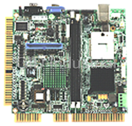
ACROSSER AR-B1420

Description
Acrosser AR-B1420 Compact 486 PC/104 CPU Module with VGA, DOC/SSD
Part Number
AR-B1420
Price
Request Quote
Manufacturer
ACROSSER
Lead Time
Request Quote
Category
Single Board Computers
Specifications
Form Factor
PC/104 Standard
BIOS
AMI Flash BIOS (128KB, including VGA BIOS)
BUS Drive Cap.
6 TTL level loads maximum
Bus Interface
Non-stack through PC/104 bus
CE Design-in
Add EMI components to COM ports, parallel port, CRT, keyboard, and PS/2 mouse
CPU & Chipset
ST STPC Client 66/75/120 MHz 486 DX CPU .(Intel 486 DX Grade)
Dimensions
90.2 mmX95.9 mm (3.55" X 3.775")
FDC
Supports two 5.25" or 3.5" floppy disk drives
Flash Disk
Supports 1 DiskOnChip socket
HDC
One PCI IDE Supports LBA/Block mode access
Indicator
Power/watchdog LED
Keyboard
PC/AT compatible keyboard
Parallel Port
1 bi-directional centronics type parallel port; Supports SPP/EPP/ECP mode
PC Board
8 layers, EMI considered
Power Req.
+5V only, 2.0A maximum
Processor
STPC 486DX
Real Time Clock
BQ3287MT or compatible chips with 128 bytes of data RAM
Serial Port
2 RS-232C/RS-485
Speaker
External speaker
VGA
Up to 4MB MB VRAM (1280X1024/256 colors)
Watchdog
Programmable watchdog timer
Features
- 2 serial ports with 16C550 UART
- 8 layer PCB
- All-In-One designed 486DX CPU card (Intel 486 DX grade)
- Bi-direction parallel interface
- Floppy disk drive interface
- IDE hard disk drive interface
- Licensed AMI BIOS
- Programmable watchdog timer
- Supports 1 SoDIMM type DRAM for 8 MB to 64 MB EDO RAM
- Supports 4 TTL inputs and 4 TTL outputs
- Supports D.O.C. up to 144MB
- Supports PC/104 bus
- Supports ST STPC Client 66/75/120 MHz (onboard 66 MHz CPU as the standard model)
Datasheet

Extracted Text
r’
Book Number: AR-B1420-99.A02
Edition: 1.2
s GuideUse
486DX CPU CARD
INDUSTRIAL GRADE
AR-B1420
¡¦
0........................................................................................................................................................0-3
COPYRIGHT NOTICE AND DISCLAIMER
WELCOME TO THE AR-B1420 CPU BOARD
BEFORE YOU USE THIS GUIDE
RETURNING YOUR BOARD FOR SERVICE
TECHNICAL SUPPORT AND USER COMMENTS
ORGANIZATION
STATIC ELECTRICITY PRECAUTIONS
1.....................................................................................................................................................1-1
INTRODUCTION
PACKING LIST
FEATURES
2.................................................................................................................................2-1
SINGLE PC CHIPSET.
PERIPHERAL CHIPSET
DMA CONTROLLER
KEYBOARD CONTROLLER
INTERRUPT CONTROLLER
I/O PORT ADDRESS MAP
MEMORY SPACE
REAL-TIME CLOCK AND NON-VOLATILE RAM
TIMER
SERIAL PORT
2.10.1Universal Asynchronous Receiver/Transmitter(UART A, UART B)
PARALLEL PORT.
3.............................................................................................................................3-1
OVERVIEW
SYSTEM SETTINGS
FDD Port Connector (CN1)
Hard Disk (IDE) Connector(CN2)
Multi-function Port Connector (CN5)
PC/104 Connector
Power / Watch Dog LED (LED1)
Serial Port
TTL Connector (J4)
Keyboard and PS/2 Mouse Connector (J1)
External Speaker Header (J2)
3.2.10Power Connector (J7)
3.2.11Reset Header (J6)
3.2.12Battery Setting
3.2.13CPU
4.ON...............................................................................................................................4-1
OVERVIEW
UTILITY DISKETTES
VGA Driver
WATCHDOG TIMER
Watchdog Timer Setting
Watchdog Timer Enabled
Watchdog Timer Trigger
Watchdog Timer Disabled
5........................................................................................................................................5-1
OVERVIEW
SWITCH SETTINGS
SOFTWARE PROGRAM
DISKONCHIP INSTALLATION
6..............................................................................................................................................6-1
BIOS SETUP OVERVIEW
STANDARD CMOS SETUP
ADVANCED CMOS SETUP
ADVANCED CHIPSET SETUP
POWER MANAGEMENT
PCI/PLUG AND PLAY
PERIPHERAL SETUP
AUTO-DETECT HARD DISKS
PASSWORD SETTING
0-1
6-12.............................................................................................................................................................6.9
6-12..................................................................................................................................................6.8
6-12...............................................................................................................................................................6.7
6-11...............................................................................................................................................................6.6
6-8............................................................................................................................................................6.5
6-7...................................................................................................................................................6.4
6-4........................................................................................................................................................6.3
6-2........................................................................................................................................................6.2
6-1..........................................................................................................................................................6.1
BIOS CONSOLE
5-2......................................................................................................................................................5.4
5-2...................................................................................................................................................MING5.3
5-1...................................................................................................................................................................5.2
5-1..................................................................................................................................................................................5.1
SOLID STATE DISK
4-5...................................................................................................................................................4.3.4
4-5......................................................................................................................................................4.3.3
4-5....................................................................................................................................................4.3.2
4-4......................................................................................................................................................4.3.1
4-4...................................................................................................................................................................4.3
4-2...........................................................................................................................................................................4.2.1
4-1..................................................................................................................................................................4.2
4-1..................................................................................................................................................................................4.1
SYSTEM INSTALLATI
3-11...............................................................................................................................................................................
3-11...............................................................................................................................................................
3-11.........................................................................................................................................................
3-10...................................................................................................................................................
3-10..........................................................................................................................................3.2.9
3-10......................................................................................................................3.2.8
3-9.............................................................................................................................................................3.2.7
3-8............................................................................................................................................................................3.2.6
3-7.........................................................................................................................................3.2.5
3-5...............................................................................................................................................................3.2.4
3-4...................................................................................................................................3.2.3
3-3........................................................................................................................................3.2.2
3-2.................................................................................................................................................3.2.1
3-2...................................................................................................................................................................3.2
3-1..................................................................................................................................................................................3.1
STEMSETTING UP THE SY
2-12................................................................................................................................................................2.11
2-9..............................................................................
2-9.........................................................................................................................................................................2.10
2-8..........................................................................................................................................................................................2.9
2-7......................................................................................................................2.8
2-6........................................................................................................................................................................2.7
2-5..........................................................................................................................................................2.6
2-4......................................................................................................................................................2.5
2-3.......................................................................................................................................................2.4
2-2...................................................................................................................................................................2.3
2-2.............................................................................................................................................................2.2
2-1................................................................................................................................................................2.1
SYSTEM CONTROLLER
1-2..................................................................................................................................................................................1.3
1-2............................................................................................................................................................................1.2
1-1.........................................................................................................................................................................1.1
OVERVIEW
0-4....................................................................................................................................0.7
0-4..........................................................................................................................................................................0.6
0-3...................................................................................................................0.5
0-3............................................................................................................................0.4
0-3...............................................................................................................................................0.3
0-3...........................................................................................................................0.2
0-3................................................................................................................................0.1
PREFACE
Table of Contents
s GuideAR-B1420 User
AARR--BB11442200 UUsseerr¡¦s¡¦s GGuuiiddee
Setting Password
Password Checking
LOAD DEFAULT SETTINGS
6.10.1Auto Configuration with Optimal Setting
6.10.2Auto Configuration with Fail Safe Setting
BIOS EXIT
6.11.1Save Settings and Exit
6.11.2Exit Without Saving
BIOS UPDATE
7...........................................................................................................................................7-1
8.........................................................................................................................8-1
8.1 PLACEMENT
DIMENSIONS
9.5................................................................................................................................9-1
10............................................................................................................................................................
0-2
10-1INDEX
PROGRAMMING RS-48
8-2..............................................................................................................................................................................8.2
8-1...............................................................................................................................................................................
SIONSPLACEMENT & DIMEN
SPECIFICATIONS
6-14.......................................................................................................................................................................6.12
6-14.......................................................................................................................................................
6-13..................................................................................................................................................
6-13.............................................................................................................................................................................6.11
6-13.....................................................................................................................
6-13.......................................................................................................................
6-13................................................................................................................................................6.10
6-13...........................................................................................................................................................6.9.2
6-13...............................................................................................................................................................6.9.1
¡¦
0.
0.1
disclaims any implied warranties of merchantability or fitness for any particular purpose. Furthermore,
Technology reserves the right to revise this publication and to make changes from time to time in the contents
Possession, use, or copying of the software described in this publication is authorized only pursuant to a valid
into any language or computer language, in any form or any means, electronic, mechanical, magnetic, optical,
…are
.
0.2
This information describes this card’s functions, features, and how to start, set up and operate your AR-B1420.
0.3
“”
of the enclosed utility diskette. It contains the modification, hardware & software information, and it has
0.4
If you need to ship your board to us for service, be sure it is packed in a protective carton. We recommend that
Ø
Ø
Ø
0.5 TECHNICAL SUPPORT AND USER COMMENTS
’s comments are always welcome as they assist us in improving the usefulness of our products and the
understanding of our publications. They form a very important part of the input used for product enhancement
0-3
Check our FAQ sheet for quick fixes to known technical problems.
webmaster@acrosser.comInternet electronic mail to:
Acrosser Technology Co., Ltd. or your local sales representative.Please send your comments to
and book number.
If you have suggestions for improving particular sections or if you find any errors, please indicate the manual title
any obligation. You may, of course, continue to use the information you supply.
We may use and distribute any of the information you supply in any way we believe appropriate without incurring
and revision.
User
And a brief description of the symptoms.
A description of the system configuration and/or software at the time is malfunction,
Include your name, address, daytime telephone and facsimile numbers and E-mail.
You can assure efficient servicing of your product by following these guidelines:
you keep the original packaging for this purpose.
If your board requires servicing, contact the dealer from whom you purchased the product for service information.
RETURNING YOUR BOARD FOR SERVICE
updates to product functions that may not be mentioned here.
. Please refer to the README.DOC fileThe AR-B1420 diskette provides the newest information about the card
the packing list. Make sure the accessories are complete.
in this guide. CheckSetting Up The SystemIf you have not already installed this AR-B1420, refer to Chapter 3,
BEFORE YOU USE THIS GUIDE
You also can find general system information here.
Acrosser AR-B1420 CPU board.This guide introduces you to the
WELCOME TO THE AR-B1420 CPU BOARD
Adobe Acrobat 3.01This document was produced with
All other trademarks and registered trademarks are the property of their respective holders.
registered trademarks., Acrosser, AMI, IBM PC/AT, ALI, Windows 3.1, MS-DOS
Acrosser Technology.chemical, manual or otherwise, without the prior written consent of
No part of this publication may be reproduced, transmitted, transcribed, stored in a retrieval system, or translated
Acrosser Technology Co., Ltd., 1999. All rights Reserved.(C) Copyright
sublicensor.Acrosser or an authorized written license from
Acrosser to this fact.
) as soon as possible, but there is no obligation on the part ofWWW.ACROSSER.COMbe posted on the Internet (
Acrosser Technology to notify any person of such revisions or changes. Changes willhereof without obligation of
Acrosser
Acrosser Technology makes no representations or warranties with respect to the contents hereof and specifically
August 1999
COPYRIGHT NOTICE AND DISCLAIMER
PREFACE
s GuideAR-B1420 User
AARR--BB11442200 UUsseerr¡¦s¡¦s GGuuiiddee
0.6
l “”
l “”
l “”
l “”
l “”
l “”
l “”
l “”
l “”
l “”
0.7
Static electricity is a constant danger to computer systems. The charge that can build up in your body may be
more than sufficient to damage integrated circuits on any PC board. It is, therefore, important to observe basic
precautions whenever you use or handle computer components. Although areas with humid climates are much
· Touch a grounded metal object to discharge the static electricity in your body (or ideally, wear a grounded
· When unpacking and handling the board or other system components, place all materials on an anti static
·
0-4
Be careful not to touch the components on the board.
surface.
wrist strap).
The following measures should generally be sufficient to protect your equipment from static discharge:
less prone to static build-up, it is always best to safeguard against accidents that may result in expensive repairs.
Before removing the board from its anti-static bag, read this section about static electricity precautions.
STATIC ELECTRICITY PRECAUTIONS
IndexChapter 10
Programming RS-485Chapter 9,
Placement & DimensionsChapter 8,
SpecificationsChapter 7,
, provides the BIOS settings and explanations.BIOS ConsoleChapter 6,
, describes the S.S.D and D.O.C InstallationSolid State DiskChapter 5,
, describes setup procedures and the utility diskette.System InstallationChapter 4,
, describes how to adjust the jumper, and the connector settings.Setting Up the SystemChapter 3,
describes the major structure.System ControllerChapter 2,
, provides an overview of the system features and packing list.OverviewChapter 1,
This manual covers the following topics (see the Table of Contents for a detailed listing):
ORGANIZATION
¡¦
1. OVERVIEW
l
l
l
1.1
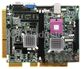
The AR-B1420 is an all-in-one 486 (PC/104) industrial grade CPU module that has been designed to withstand
continuous operation in harsh environments. This board can stand alone as a CPU card or be used with other
The 8 layer PCB CPU card is equipped with an IDE HDD interface, a floppy disk drive adapter, 1 parallel port, 2
serial ports and a watchdog timer. Its dimensions are as compact as 90.2mm X 95.9mm. Its highly condensed
modules from hundreds of venders around the world. You can also directly connect the power supply to the AR-
A watchdog timer, which has a software programmable time-out interval, is also provided on this CPU card. It
A super I/O chip (W83977) is embedded in the AR-B1420 card. It combines the functions of a floppy disk drive
adapter, two serial (with 16C550 UART) adapters and 1 parallel adapter in one chip. The I/O port configurations
a MODEM, and parallel to serial conversions on data character received from the CPU. The UART includes a
The VGA controller also supports CRT color monitors. It can be connected to create a compact video solution for
1-1
the industrial environment.
-type printer interface.centronicsbi-directional parallel user with a fully
programmable baud rate generator, and a processor interrupt system. As a parallel port, the W83977 provides the
As a UART, the chip supports serial to parallel conversions on data characters received from a peripheral device or
can be set up in BIOS setup program.
ensures that the system does not hang-up if a program can not execute normally.
B1420 on-board power connector in standalone applications.
with the addition of an adapter. Based on the PC/104 expansion bus, you could easily install thousands of PC/104
The AR-B1420 provides 1 bus interface: a PC/104 compatible expansion bus, which can be turned into an ISA bus
speed and mean time between failures is critical.
features make it an ideal cost/performance solution for high-end commercial and industrial applications where CPU
SoDIMM.using any 144-pin type
PC/104 compatible cards. The total on-board memory for the AR-B1420 can be configured from 8MB to 144MB by
INTRODUCTION
Features
Packing List
Introduction
This chapter provides an overview of your system features and capabilities. The following topics are covered:
s GuideAR-B1420 User
AARR--BB11442200 UUsseerr¡¦s¡¦s GGuuiiddee
1.2 PACKING LIST
l
l
l
l
l
l
l
l
l
1.3
This system provides a number of special features that enhance its reliability, ensure its availability, and improve
l
l
l
l
l
l
l
l
l
l
l
l
l
1-2
8 layer PCB.
Supports 4 TTL inputs and 4 TTL outputs
Programmable watchdog timer.
2 serial ports with 16C550 UART.
Bi-direction parallel interface.
drive interface.Floppy disk
disk drive interface.IDE hard
Licensed AMI BIOS.
Supports D.O.C. up to 144MB.
SoDIMM type DRAM for 8 MB to 64 MB EDO RAMSupports 1
Supports PC/104 bus.
Supports ST STPC Client 66/75/120 MHz (onboard 66 MHz CPU as the standard model)
All-In-One designed 486DX CPU card (Intel 486 DX grade)
its expansion capabilities, as well as its hardware structure.
FEATURES
1 kit of screws
1 power cable
1 Software utility diskette
1 keyboard/ PS/2 mouse adapter cable
1 4-in-1 adapter cable for COM1/COM2, parallel, and VGA
1 Floppy disk drive interface cable(2.54 mm pin pitch)
1 Hard disk drive interface cable (2.0 mm pin pitch)
1 AR-B1420 CPU card
The quick setup guide
to make sure that the following items have been included inside the AR-B1420 package:
These accessories are included with the system. Before you begin installing your AR-B1420 board, take a moment
¡¦
2.
This chapter describes the major structure of the AR-B1420 CPU board. The AR-B1420 is mainly composed of a
BIOS
I/O
2.1 SINGLE PC CHIPSET
The single PC Chipset integrates a fully static X86 processor, which is fully compatible with X86 processors and
device is packaged in a 388 Ball Grid Array (PBGA). At the heart of the Single PC Chipset is an advanced 64-bit
controller, advanced 64-bit accelerated graphics and video controller, a high speed PCI local-bus controller and
industry standard PC chip set functions (interrupt controller, DMA controller, interval timer and ISA bus) and an
The single PC Chipset makes use of a tightly coupled Unified Memory Architecture (UMA), where the same
memory array is used for CPU main memory and graphics frame-buffer. This means a reduction in total system
memory for system performances that are equal to that of a comparable frame buffer and system memory based
system. System performance is also generally improved, due to the higher memory bandwidth allowed by
attaching the graphics engine directly to 64-bit processor host interface running at the speed of the processor bus
rather than the traditional PCI bus. Graphics functions are controller through the on chip graphics engine and the
monitor display is produced through the 2D graphics display engine. The graphics resolution supported is a
maximum of 1280X1024 at a 75Hz refresh rate and is VGA and SVGA compatible. Horizontal timing fields are
The 64-bit wide memory array provides the system with 200Mb/s bandwidth, double that of an equivalent 32-bit
The standard PC chipset functions (DMA, Interrupt controller, timers, power management logic) are
2-1
integrated
system. This allows for higher resolution screens and greater color depth.
frame buffer can occupy a space anywhere in the first four Mbytes of physical main memory.
VGA compatible while the vertical fields are extended by one bit to accommodate the above display resolution. The
EIDE controller.
processor block, dubbed the 5ST86. The 5ST86 includes a powerful X86 processor core along with a 64-bit DRAM
device. The performance of the device is comparable with the performance of a typical P5 generation system. This
combines with a powerful chipset, graphics and video pipelines to provide a PC compatible subsystem on a single
Figure 2-1 System Block Diagram
JP2
CN1
J1
JP1
JP4JP4CN1
RS485KEY
U7
RS-232/PS/2
UARTPrintFDD
CN4
U4
CN3
U27
U3J4
104
Peripheral chipset
SSDTTLPC
ISA BUS
J2SPEAKER
IDE
CN2
chipset
DRAM
CPU
JP4DISPLAY
RESET
J6
ChipSet and a Peripheral Chipset. A functional block diagram follows.Single PC
SYSTEM CONTROLLER
s GuideAR-B1420 User
AARR--BB11442200 UUsseerr¡¦s¡¦s GGuuiiddee
2.2 PERIPHERAL CHIPSET
The peripheral Chipset on AR-B1420 integrates the disk driver adapter, serial port (UART), parallel port
The disk driver adapter functions include a floppy disk driver controller compatible with the industry standard
driver interface control logic, and interrupt/ DMA logic. The wide range of functions are integrated onto one chip
supports up to four 360K, 720K, 1.2M, 1.44M, or 2.88M disk drives and data transfer rates of 250 Kb/s, 300 Kb/s,
complete modem control capability, and a processor interrupt system. Both UARTs provide legacy speed with
which support higher
The Peripheral Chipset supports one PC–Compatible printer port (SPP), Bi-directional printer port (BPP) and also
The configuration registers support mode selection, function enable/disable, and power down function selection.
Furthermore, the configurable PnP features are compatible with the Windows 95™ plug-and-play, which makes
The keyboard controller is based on an 8042 compatible instruction set with a 2K Byte programmable ROM and a
256-Byte RAM bank. Keyboard BIOS firmware is available with optional AMIKEY-2, Phoenix MultiKey/42, or
The Peripheral Chipset provides a set of flexible I/O control functions to system designer through a set of
purpose I/O ports. These GPIO ports may serve as simple I/O or may individually be configured to provide a pre-
defined alternate function. The Peripheral Chipset is made to fully comply with the Microsoft™ PC97 Hardware
2.3 DMA CONTROLLER
AR-B1420 board. Each controller is a four-channel DMA device that will generate the memory addresses and
transfer with less CPU intervention. The two DMA controllers are internally cascaded to provide
four DMA channels for transfers to 8-bit peripherals (DMA1) and three channels for transfers to 16-bit peripherals
(DMA2). DMA2 channel 0 provides the cascade interconnection between the two DMA devices, thereby
2-2
maintaining IBM PC/AT compatibility.
speed information
peripheral device and memory. This allows high-control signals necessary to transfer information directly between a
The equivalent of two 8237AT compatible DMA controllers built into the Single PC Chipset are implemented on the
DMAs, I/O space resources are flexible to meet ISA PnP requirements.IRQs, Design Guide and
general
customer code.
system resource allocation more efficient than ever.
Enhanced Parallel Port (EPP) and Extended Capabilities Port (ECP).
speed modems. In addition, on the AR-B1420 board dual RS-485 ports are offered.
bpsbaud rate 115.2K and provide advanced speed with baud rates of 230k, 460k, and 921k
, a programmable baud rate generator,infrared communication. Each UART includes a 16-byte send/receive FIFO
UARTs), one of which supports serialThe Peripheral Chipset provides two high-speed serial communication ports (
500 Kb/s, 1Mb/s, and 2 Mb/s.
greatly reduces the number of components required for interfacing with floppy disk drivers. This disk driver adapter
82077/765, a data separator, a write pre-compensation circuit, decode logic, data rate selection, a clock generator,
mouse support , Real Time Clock,14 general purpose I/O ports, and full 16-bit address decoding.
,8042 keyboard controller with PS/2configurable plug-and-play registers in one chip, plus additional features: ACPI
An EIDE port is provided for storage devices such as hard disks and CD-ROMs, bridging directly to the PCI bus.
Additional functions are accessed by the single PC Chipset via the ISA bus.together with the X86 processor core.
¡¦
2.4 KEYBOARD CONTROLLER
The KBC circuit of the peripheral chipset is designed to provide the functions needed to interface a CPU with a
keyboard and/or a PS/2 mouse, and can be used with IBM®-compatible personal computers orPS/2-based
systems. The controller receives serial data from the keyboard or PS/2 mouse, checks the parity of the data, and
the system when data is placed in its output buffer. The keyboard and PS/2 mouse are required to acknowledge
all data transmissions. No transmission should be sent to the keyboard or PS/2 mouse until an acknowledge is
KIRQ
8042
2-3
Keyboard and Mouse InterfaceFigure 2-2
P11
MDAT
P22
Multiplex I/O PINS
T1
P12 ~P16
GPI/O PINS
MCLK
P23
T0
KCLK
P26
P10
KDAT
P27
KBRST
P20
GATEA20
P21
P17KINH
MIRQ
P25
P24
received for the previous data byte.
presents the data to the system as a byte of data in its output buffer. Then, the controller will assert an interrupt to
DMA Channel ControllerTable 2-1
Channel 7(3): SpareChannel 3: Spare
Channel 6(2): SpareChannel 2: Diskette adapter
Channel 5(1): SpareChannel 1: IBM SDLC
Channel 4(0): Cascade for controller 1Channel 0: Spare
DMA Controller 2DMA Controller 1
chnlsMaster with three 16-bit chnlsSlave with four 8-bit
The Following is the system information for the DMA channels:
s GuideAR-B1420 User
AARR--BB11442200 UUsseerr¡¦s¡¦s GGuuiiddee
2.5 INTERRUPT CONTROLLER
The equivalent of two 8259 Programmable Interrupt Controllers (PIC) are included on the AR-B1420 board. They
CPU, and provide vectors which are used as acceptance indices by the CPU to determine which interrupt service
routine to execute. These two controllers are cascaded with the second controller representing IRQ8 to IRQ15,
2
2-4
IRQ14 and IRQ15 are configured for the Hard Disk adapter only and can not be used for other devices.Note:
Figure 2-3 Interrupt Controller
Parallel port 1IRQ 7
IRQ 6
Floppy disk adapter
IRQ 5
Reserved
Serial port 1IRQ 4
Serial port 2IRQ 3
: Hard disk adapterIRQ15
: Hard disk adapterIRQ14
coprocessor : Math.IRQ13
: Reserved for PS/2 mouseIRQ12
: ReservedIRQ11
: ReservedIRQ10
: ReservedIRQ9
: Real time clockIRQ8
Rerouting to IRQ8 to IRQ15
IRQ
Keyboard output buffer fullIRQ 1
IRQ 0
timer interrupt from timer 8253System
CTRL1
CTRL2
NMI
Parity check
InInterrupt Level
Description
The following is the system information of interrupt levels:
which is rerouted through IRQ2 on the first controller.
accept requests from peripherals, resolve priorities on pending interrupts in service, issue interrupt requests to the
¡¦
2.6
2-5
Table 2-2 I/O Port Address Map
TTL IO port216-217
SSD IO port210-211
Serial port 1 (COM 1)3F8-3FF
Diskette controller3F0-3F7
Serial port 3 (COM 3)3E8-3EF
Color/graphics monitor adapter3D0-3DF
EGA/VGA adapter3C0-3CF
Monochrome display and printer port 3 (LPT 3)3B0-3BF
Bisynchronous3A0-3AF
SDLC, bisynchronous380-38F
Parallel printer port 1 (LPT 1)378-37F
LAN adapter320-33F
Prototype card/streaming type adapter300-31F
Serial port 2 (COM 2)2F8-2FF
Serial port 4 (COM 4)2E8-2EF
Parallel printer port 2 (LPT 2)278-27F
EMS register 1218-21A
EMS register 0208-20A
Game port201
Fixed disk 01F0-1F8
Fixed disk 1170-178
Math Co-processor0F8-0FF
Reset Math Co-processor0F1
Clear Math Co-processor0F0
DMA controller 20C0-0DF
Interrupt controller 20A0-0A1
DMA page registers080-09F
maskable interrupt (NMI)Real-time clock (RTC), non-070-071
8042 keyboard/controller060-06F
Timer 2050-05F
Timer 1040-04F
STPC Client Address022-023
Interrupt controller 1020-021
DMA controller 1000-01F
DeviceHex Range
I/O PORT ADDRESS MAP
s GuideAR-B1420 User
AARR--BB11442200 UUsseerr¡¦s¡¦s GGuuiiddee
2.7
System Memory Used by DOS and
“”“”
“”
“”“”
“X”
DEVICE=C:\DOS\EMM386.EXE x=C800-C9FF
“”
“”
ON
OFF
1234
“”
“”
ON
OFF
1234
“”
“”
ON
OFF
1234
“”
“”
ON
OFF
1234
2-6
Table 2-4 SW1 Switch Setup
8KD2000~D4000D.O.C. Data Bank
ONSwitch4 set to
8KD0000~D2000S.S.D Data BankONSwitch 3 set to
8KCA000~CC000D.O.C Data Bank
ONSwitch4 set to
8KC8000~CA000S.S.D Data BankOFFSwitch 3 set to
OFFSwitch 4 set to
8KD0000~D2000S.S.D Data BankONSwitch 3 set to
OFFSwitch 4 set to
8KC8000~CA000S.S.D Data BankOFFSwitch 3 set to
Extra Memory SizeMemory MapMemorySW1
:0)CONFIG.SYS file write as: (if the memory configuration of AR-B1420 is C800
particular range of segment address, which is used by AR-B1420, for an EMS page. For example, the line in
option to prevent EMM386.EXE from using a If you have installed EMM386.EXE driver, please use the Note 3:
table exhibits the SW1 switch setup.
Simultaneously, this setup will occupy extra 8K-memory size. Also Refer to Chapter 5 Solid State Disk. The following
ON. should be set to SW1 Switch 4 When the system uses D.O.C. flash memory, the hardware Note 2:
Refer to Chapter 5 Solid State Disk.Switch 3.SW1
by means of manual switchD0000~D2000 or C8000~CA000 You can set up the S.S.D. data bank at either Note 1:
Table 2-3 Memory Space
System Extension Memory0100000-FFFFFFF
System BIOS ROM00F0000-00FFFFF
Reserved for PCI Device ROM00E0000-00EFFFF
RAM Buffer
Reserved for I/O Device BIOS ROM or00C0000-00DFFFF
CGA/ MONOCHROME adapter
Display Buffer Memory for VGA/ EGA/00A0000-00BFFFF
Application
0000000-009FFFF
AssignmentMemory Map
MEMORY SPACE
¡¦
2.8
The RTC with 242 bytes of RAM is a low-power device that provides a time-of-day clock in various formats and a
R/W
R/W
R/W
R/W
R/W
R/W
R/W
R/W
R/W
R/W
R/W
R/W
R
R
R/W
R/W
2-7
Table 2-6 Real Time Clock Address Map Bank 1
Register 0h-7fh00h-7Fh
REGISTER FUNCTIONREGISTER TYPEADDRESS
Table 2-5 Real Time Clock Address Map Bank
Register 0Eh-7Fh: USER RAM0Eh-7Fh
Register 0Dh: Status Register0Dh
Register 0Ch: Status Register0Ch
(Bit 0 is Read Only)
Register 0Bh: Control Register0Bh
Register 0Ah: Control Register0Ah
Register 09h: Year09h
Register 08h: Month08h
Register 07h: Date of Month07h
Register 06h: Day of Week06h
Register 05h: Hours Alarm A05h
Register 04h: Hours04h
Register 03h: Minutes Alarm A03h
Register 02h: Minutes02h
Register 01h: Seconds Alarm A01h
Register 00h: Seconds00h
REGISTER FUNCTIONREGISTER TYPEADDRESS
calendar with century register. It has 2 alarms.
REAL-TIME CLOCK AND NON-VOLATILE RAM
s GuideAR-B1420 User
AARR--BB11442200 UUsseerr¡¦s¡¦s GGuuiiddee
2.9
2-8
Application programs can load different counts into this timer to generate various sound frequencies.
This timer provides the speaker tone.Timer 2
This timer is used to trigger memory refresh cycles.Timer 1
The output of this timer is tied to interrupt request 0. (IRQ 0)Timer 0
The AR-B1420 provides three programmable timers, each with a timing frequency of 1.19 MHz.
TIMER
¡¦
2.10 SERIAL PORT
2.10.1
UARTs are used to convert parallel data into serial format on the transmit side and convert serial data to
by five to eight data bits, a parity bit (if programmed) and one, one and half (five-bit format only) or two stop bits.
UARTs are capable of handling divisors of 1 to 65535 and producing a 16x clock for driving the internal
transmitter logic. Provisions are also included to use this 16x clock to drive the receiver logic. The UARTs also
support the MIDI data rate. Furthermore, the UARTs also include complete modem control capability and a
processor interrupt system that may be software trailed to the computing time required to handle the
UARTs have a FIFO mode to reduce the number of interrupts presented to the CPU. In
0
0
X
X
X
X
X
X
1
1
“0”
2-9
Bit 7: Must be 0
Bit 6: Must be 0
Bit 5: Must be 0
Bit 4: Must be 0
Bit 3: Must be 0
Bit 2: Interrupt ID Bit 1
Bit 1: Interrupt ID Bit 0
if Interrupt PendingBit 0:
(4) Interrupt Identification Register (IIR)
Bit 7: Must be 0
Bit 6: Must be 0
Bit 5: Must be 0
Bit 4: Must be 0
Bit 3: Enable MODEM Status Interrupt (EDSSI)
Bit 2: Enable Receiver Line Status Interrupt (ELSI)
Bit 1: Enable Transmitter Holding Empty Interrupt (ETBEI)
Bit 0: Enable Received Data Available Interrupt (ERBFI)
(3) Interrupt Enable Register (IER)
Bit 0-7: Transmitter holding data byte (Write Only)
(2) Transmitter Holding Register (THR)
Bit 0-7: Received data byte (Read Only)
(1) Receiver Buffer Register (RBR)
Table 2-7 ACE Accessible Registers
Divisor latch (most significant byte)base + 1
Divisor latch (least significant byte)base + 0
Scratched registerbase + 7
MODEM statusbase + 6
Line statusbase + 5
MODEM controlbase + 4
Line controlbase + 3
Interrupt identification (read only)base + 2
Interrupt enablebase + 1
Transmitter holding register (write)
Receiver buffer (read)base + 0
RegisterPort AddressDLAB
The following table is summary of each ACE accessible register
..FIFOs for both receive and transmit modeeach UART, there are 16-byte
communication link. The
The
parallel format on the receiver side. The serial format, in order of transmission and reception, is a start bit, followed
The
Universal Asynchronous Receiver/Transmitter(UART A, UART B)
s GuideAR-B1420 User
AARR--BB11442200 UUsseerr¡¦s¡¦s GGuuiiddee
005 Bits
016 Bits
107 Bits
118 Bits
2-10
Bit 7: Received Line Signal Detect (RSLD)
Bit 6: Ring Indicator (RI)
Bit 5: Data Set Ready (DSR)
Bit 4: Clear to Send (CTS)
Bit 3: Delta Receive Line Signal Detect (DSLSD)
Bit 2: Training Edge Ring Indicator (TERI)
Bit 1: Delta Data Set Ready (DDSR)
Bit 0: Delta Clear to Send (DCTS)
(8) MODEM Status Register (MSR)
Bit 7: Must be 0
Bit 6: Transmitter Shift Register Empty (TSRE)
Bit 5: Transmitter Holding Register Empty (THRE)
Bit 4: Break Interrupt (BI)
Bit 3: Framing Error (FE)
Bit 2: Parity Error (PE)
Bit 1: Overrun Error (OR)
Bit 0: Data Ready (DR)
(7) Line Status Register (LSR)
Bit 7: Must be 0
Bit 6: Must be 0
Bit 5: Must be 0
Bit 4: Loop
Bit 3: Out 2 (OUT 2)
Bit 2: Out 1 (OUT 1)
Bit 1: Request to Send (RTS)
Bit 0: Data Terminal Ready (DTR)
(6) MODEM Control Register (MCR)
Bit 7: Divisor Latch Access Bit (DLAB)
Bit 6: Set Break
Bit 5: Stick Parity
Bit 4: Even Parity Select (EPS)
Bit 3: Parity Enable (PEN)
Bit 2: Number of Stop Bit (STB)
Word LengthWLS0WLS1
Bit 1: Word Length Select Bit 1 (WLS1)
Bit 0: Word Length Select Bit 0 (WLS0)
(5) Line Control Register (LCR)
¡¦
MS
Bit 0Bit 8
Bit 1Bit 9
Bit 2
Bit 3
Bit 4
Bit 5
Bit 6
Bit 7
8
6
4
3
2
1
2-11
Table 2-8 Serial Port Divisor Latch
115200
57600
38400
28800
19200
14400
129600
244800
323600
482400
641800
961200
192600
384300
Divisor Used to Generate 16x ClockDesired Baud Rate
Bit 15Bit 7:
Bit 14Bit 6:
Bit 13Bit 5:
Bit 12Bit 4:
Bit 11Bit 3:
Bit 10Bit 2:
Bit 1:
Bit 0:
LS
(9) Divisor Latch (LS, MS)
s GuideAR-B1420 User
AARR--BB11442200 UUsseerr¡¦s¡¦s GGuuiiddee
2.11 PARALLEL PORT
’
The parallel portion of the W83977 makes the attachment of various devices that accept eight bits of parallel data
’
76543210
XXX
This signal may become active during data entry, when the printer is off-line during printing, or when the
print head is changing position or in an error state. When Bit 7 is active, the printer is busy and can not
This bit represents the current state of the printer’s ACK signal. A 0 means the printer has received the
character and is ready to accept another. Normally, this signal will be active for approximately 5
2-12
A 0 means the printer has encountered an error condition.Bit 3:
A 1 means the printer is selected.Bit 4:
A 1 means the printer has detected the end of the paper.Bit 5:
a BUSY message stops.microseconds before receiving
Bit 6:
accept data.
Bit 7:
X represents not used.NOTE:
Figure 2-4 Printer Status Buffer
-BUSY
-ACK
PE
SLCT
-ERROR
definitions are described as follows:
The system microprocessor can read the printer status by reading the address of the Printer Status Buffer. The bit
(4) Printer Status Buffer
the Data Swapper address.
s Data Latch through the Data Swapper by readingThe system microprocessor can read the contents of the printer
(3) Data Swapper
at standard TTL level.
(2) Printer Interface Logic
AddressTable 2-9 Registers
Printer control latchWritebase + 2
Printer status bufferReadbase + 1
Input dataReadbase + 0
Output dataWritebase + 0
RegisterRead/WritePort Address
(1) Register Address
¡¦
The system microprocessor can read the contents of the printer control latch by reading the address of printer
76543210
XX
’
A 0.5 microsecond minimum highly active pulse clocks data into the printer. Valid data must be present
2-13
for a minimum of 0.5 microseconds before and after the strobe pulse.
Bit 0:
A 1 causes the printer to line-feed after a line is printed.Bit 1:
A 0 starts the printer (50 microseconds pulse, minimum).Bit 2:
A 1 in this bit position selects the printer.Bit 3:
A 1 in this position allows an interrupt to occur when ACK changes from low state to high state.Bit 4:
. This bit is write only.from external sources to be read; when logic 0, they work as a printer port
Direction control bit. When logic 1, the output buffers in the parallel port are disabled allowing data drivenBit 5:
X represents not used.NOTE:
s DefinitionFigure 2-5 Bit
DIR(write only)
IRQ ENABLE
SLDC IN
INIT
AUTO FD XT
STROBE
control swapper. Bit definitions are as follows:
(5) Printer Control Latch & Printer Control Swapper
s GuideAR-B1420 User
¡¦
3.
’
l
l
3.1
e’s’
J2
2
CN1 J31234
J4
1
J6
2
1
1
21
3-1
Figure 3-1 AR-B1420 Jumpers & Connectors Placement
J7
CN3AR-B1420 V1.1
40
39
63
J6
64
CN4
H5
CN2
CN5
U5
U3
JP3
J5
OFF
JP2
J4
SW1
JP1
J2
LED1J3J1CN1
assignments.
locations, and the pins jumper settings, the connectorharsh environments. This section provides the hardwar
The AR-B1420 is a PC/104 industrial grade CPU card that has been designed to withstand continuous operation in
OVERVIEW
System Settings
Overview
s external connectors and the jumper settings.This section describes pin assignments for the system
SETTING UP THE SYSTEM
s GuideAR-B1420 User
AARR--BB11442200 UUsseerr¡¦s¡¦s GGuuiiddee
3.2
Jumper pins allow you to set specific system parameters. Set them by changing the pin location of the jumper
blocks. (A jumper block is a small plastic-encased conductor that slips over the pins.)
remove the jumper from its current location with your fingers or small needle-nosed pliers. Place the jumper over
Do not touch any electronic component unless you are safely grounded. Wear a grounded wrist strap
3.2.1 FDD Port Connector (CN1)
Ground 12 DRVEN 0
Ground 34 Not Used
Ground 56 DRVEN 1
Ground 78 -INDEX
Ground 910 -MTR 0
Ground 1112 -DRV 1
Ground 1314 -DRV0
Ground 1516 -MTR1
Ground 1718 DIR
Ground 1920 -STEP
Ground 2122 -WDATA
Ground 2324 -WGATE
Ground 2526 -TRK 0
Ground 2728 -WRPT
Ground 2930 -RDATA
Ground 3132 -HDSEL
Ground 3334 DSKCHG
2
3-2
CN1: FDD Port connectorFigure 3-
To enable or disable the floppy disk controller, please use the BIOS Setup program.
for supporting up to two floppy disk drives.The AR-B1420 provides a 34-pin header type connector
permanently damage electronic components.
or touch an exposed metal part of the system unit chassis. The static discharges from your fingers can
CAUTION:
We will show the locations of the AR-B1420 jumper pins, and the factory-default settings in section 3.2.
pins.
the two pins designated for the desired setting. Press the jumper evenly onto the pins. Be careful not to bend the
setting, To change a jumper
SYSTEM SETTINGS
¡¦
3.2.2 Hard Disk (IDE) Connector(CN2)
A 44-pin header type connector (CN2) is provided to interface with up to two embedded hard disk drives (IDE AT
“”
To enable or disable the hard disk controller, please use the BIOS Setup program. The following table illustrates
e’
CN2
-IDERST 12 GROUND
8 D10
10 D11
D3 1112 D12
D2 1314 D13
D1 1516 D14
D0 1718 D15
GROUND 1920 Not Used
Used 2122 GROUND
24 GROUND
-IOR 25
26 GROUND
-IORDY 2728 Not Used
30 GROUND
Not Used 29
IRQ 14 3132 -IO16
HDA1 3334 Not Used
HDA0 3536 HDA2
-HDCS0 3738 -HDCS1
-HDLED 3940 GROUND
VCC 4142 VCC
GROUND 4344 Not Used
3-3
Figure 3-3 CN2: Hard Disk (IDE) Connector
-IOW 23
Not
D4 9
D5 7
6 D9D6 5
4 D8D7 3
s 44-pin connector.the pin assignments of the hard disk driv
fashion.daisy chainbus). This interface, through a 44-pin cable, allows the user to connect up to two drives in a
s GuideAR-B1420 User
AARR--BB11442200 UUsseerr¡¦s¡¦s GGuuiiddee
3.2.3 Multi-function Port Connector (CN5)
Pin10 are COM1 signals. Pin11 to Pin 20 are COM2 signals. Pin21 to Pin 40 are Parallel port signals. Pin41 to
DCD1 12 DSR1
RXD1 3
TXD1 5
COM1
10 CASE GND
DCD2 1112 DSR2
RXD2 1314 RTS2
TXD2 1516 CTS2
COM2
DTR2 1718 R12
GND 1920 GND
-Strobe 2122 -Auto Form Feed
Data 0 2324 Error
Data 1 2526 -Initialize
Data 2 2728 -Printer Select In
Data 3 2930 Data 4
Data 5 3132 Data 6
Data 7 3334 -Acknowledge
Busy 3536 Paper
GND 3738 Printer Select
GND 3940 GND
Red 4142 VGA GND
Green 4344 GND
Blue 4546 GND
Horizontal Sync 4748 DDC DATA
Vertical Sync 4950 DDC CLOCK
3-4
Figure 3-4 CN5: Multi-function Port Connector
VGA
Parallel
GND 9
8 R11DTR1 7
6 CTS1
4 RTS1
characteristics (different drivers for different modes) to display the mode you want.
The AR-B1420 supports CRT color monitors. For different VGA display modes, your monitor must possess certain
connector. This adapter is included in your AR-B1420 package.
4-IN-1 adapter cable has to be connected to the CN5 (50-pin header type)Pin 50 are VGA port signals. To use it, a
CN5 integrates COM1/ COM2, the Parallel (Printer) port, and the VGA port into a single 50-pin connector. Pin1 to
¡¦
3.2.4 PC/104 Connector
2
164-Pin PC/104 Connector
CN4
12
-IOCHCK ------ GND
SD7 ---
SD6 ---
--- +5 VDC
SD5 ------ IRQ9
SD4 ---
--- -5 VDC
SD3 ------ DRQ2
SD2 ---
--- -12 VDC
SD1 ------ -ZWS
SD0 ---
--- +12 VDC
-IOCHRDY---A10B10
--- GND
AEN ---A11B11--- -SMEMW
SA19 ---A12B12
--- -SMEMR
SA18 ---A13B13--- -IOW
SA17 ---A14B14--- -IOR
SA16 ---A15B15
--- -DACK3
SA15 ---A16B16--- DRQ3
SA14 ---A17B17
--- -DACK1
SA13 ---A18B18
--- DRQ1
SA12 ---A19B19--- -REFRESH
SA11 ---A20B20
--- BUSCLK
SA10 ---A21B21--- IRQ7
SA9 ---A22B22 --- IRQ6
SA8 ---A23B23--- IRQ5
SA7 ---A24B24--- IRQ4
SA6 ---A25B25--- IRQ3
SA5 ---A26B26--- -DACK2
SA4 ---A27B27--- TC
SA3 ---A28B28--- BALE
SA2 ---A29B29--- +5 VDC
SA1 ---A30B30--- OSC
SA0 ---A31B31--- GND
GND ---A32B32--- GND
1
2
7
CN3
12
8
3-5
CN3: 40-Pin PC/104 Connector Bus C & D SignalFigure 3-
--- GNDD20C20Not Used ---
--- GND
D19C19SD15 ---
--- -MASTER
D18C18SD14 ---
--- +5 VDCD17C17SD13 ---
--- DRQ7
D16C16SD12 ---
--- -DACK7D15C15SD11 ---
--- DRQ6
D14C14SD10 ---
--- -DACK6D13C13SD9 ---
--- DRQ5
D12C12SD8 ---
--- -DACK5
D11C11-MEMR ---
--- DRQ0D10C10-MEMW ---
--- -DACK0
D9C9LA17 ---
--- IRQ14D8C8LA18 ---
--- IRQ15
D7C7LA19 ---
--- IRQ12D6C6LA20 ---
--- IRQ11
D5C5LA21 ---
--- IRQ10
D4C4LA22 ---
--- -IOCS16D3C3LA23 ---
--- -MEM16
D2C2-SBHE ---
--- GNDD1C1GND ---
CN3: 40 Pin PC/104 Connector Bus C & DFigure 3-
40 Pin PC/104 Connector
40
39
(2) 40 Pin PC/104 Connector Bus C & D (CN3)
Figure 3-6 CN4: 64-Pin PC/104 Connector Bus A & B Signal
B9A9
B8A8
B7A7
B6A6
B5A5
B4A4
B3A3
--- RSTDRV
B2A2
B1A1
Figure 3-5 CN4: 64 Pin PC/104 Connector Bus A & B
63
64
(1) 64 Pin PC/104 Connector Bus A & B (CN4)
s GuideAR-B1420 User
AARR--BB11442200 UUsseerr¡¦s¡¦s GGuuiiddee
AEN [output]The DMA Address Enable is high when the DMA controller
is driving the address bus. It is low when the CPU is driving
the address bus
BALE [Output]The Buffered Address Latch Enable is used to latch SA0 -
SA19 onto the falling edge. This signal is forced high
during DMA cycles
BUSCLK [Output]The BUSCLK signal of the I/O channel is asynchronous to
the CPU clock.
-DACK 0-3, 5-7The DMA Acknowledges 0 to 3, 5 to 7 are the
[Output]corresponding acknowledge signals for DRQ 0 to 3 and 5
to 7
DRQ 0-3, 5-7 [Input]DMA Request channels 0 to 3 are for 8-bit data transfers.
DMA Request channels 5 to 7 are for 16-bit data transfers.
DMA request should be held high until the corresponding
DMA has been completed. DMA request priority is in the
following sequence:(Highest) DRQ 0, 1, 2, 3, 5, 6, 7
(Lowest)
-IOCHCK [Input]The I/O Channel Check is an active low signal which
indicates that a parity error exist on the I/O board
IOCHRDYThis signal lengthens the I/O, or memory read/write cycle,
and should be held low with a valid address
-IOCS16The I/O Chip Select 16 indicates that the present data
transfer is a 1-wait state, 16-bit data I/O operation
-IORThe I/O Read signal is an active low signal which instructs
[Input/Output]the I/O device to drive its data onto the data bus
-IOWInput/Output]The I/O write signal is an active low signal which instructs
the I/O device to read data from the data bus
The Interrupt Request signal indicates I/O service request
[Input]attention. They are prioritized in the following sequence :
(Highest) IRQ 9, 10, 11, 12, 13, 15, 3, 4, 5, 6, 7 (Lowest)
LA17 - LA23The Unlatched Address line run from bit 17 to 23
Input/Output]
-MASTER [Input]The MASTER is the signal from the I/O processor which
gains control as the master and should be held low for a
maximum of 15 microseconds or system memory may be
lost due to the lack of refresh
-MEMCS16The Memory Chip Select 16 indicates that the present data
transfer is a 1-wait state, 16-bit data memory operation
-MEMRThe Memory Read signal is low while any memory location
[Input/Output]is being read
-MEMWThe Memory Write signal is low while any memory location
[Input/Output]is being written
[Output]The Oscillator is a 14.31818 MHz signal used for the color
graphic card
-REFRESHThis signal is used to indicate a memory refresh cycle and
[Input/Output]can be driven by the microprocessor on the I/O channel
RSTDRV [Output]This signal goes high during power-up, low line-voltage or
hardware reset
SA0 - SA19The System Address lines run from bit 0 to 19. They are
[Input / Output]latched onto the falling edge of "BALE"
SBHEInput/Output]The System Bus High Enable indicates the high byte SD8 -
SD15 on the data bus
3-6
[
OSC
[Input, Open collector]
[
IRQ 3-7, 9-12, 14, 15
[
[Input, Open collector]
[Input, Open collector]
DescriptionName
(3) PC/104 Channel Signal Description
¡¦
SD0 - SD15System Data bit 0 to 15
Input/Output]
-SMEMRThe System Memory Read is low while any of the low 1
mega bytes of memory are being used
-SMEMWThe System Memory Write is low while any of the low 1
mega bytes of memory is being written
TCTerminal Count provides a pulse when the terminal count
for any DMA channel is reached
-ZWSThe Zero Wait State indicates to the microprocessor that
the present bus cycle can be completed without inserting
an additional wait cycle
’
3.2.5 Power / Watch Dog LED (LED1)
The AR-B1420 provides a rectangular LED indicator to indicate the status of the Power/ Watch Dog. LED1 is
3-7
located at the upper right corner of the board above the 50-pin multi-function port connector.
s DescriptionTable 3-1 I/O Channel Signal
[Input, Open collector]
[Output]
[Output]
[Output]
[
DescriptionName
s GuideAR-B1420 User
AARR--BB11442200 UUsseerr¡¦s¡¦s GGuuiiddee
3.2.6 Serial Port
ON
OFF
1234
9
1. The recommended configuration for the RS-485 interface is to set the transmitter to be controlled by
ON
OFF
1234
246
135
12
34
56
3-8
J4: RS-485 Terminator Select12Figure 3-
Off: disabled
On: enabled
JP2JP2
JP1JP1
1 21 2
(Factory Default Setting)
RS-485 may need to be terminated when there are multiple blocks on one line.
(3) RS-485 Terminator Select (JP1/JP2)
Table 3-2 RS-485 Pin Assignments
GNDGND
BNET-ANET-
BNET+ANET+
SignalJ3SignalJ3
J3: RS-485 Pin Jack Assignment11Figure 3-
6 GND
5 GND
4 BNET-
3 ANET-
2 BNET+
1 ANET+
COM2: RS-485/RS-422 Connector10Figure 3-
(Factory Default Setting)Off: RS-232
On: RS-485
SW1- Switch 2
(2) COM2: RS-232/RS-485 Select (SW1-Switch2)
then disabled.DTR to set the transmitter. The receiver is
NOTE:
COM1: RS-485/RS-422 ConnectorFigure 3-
(Factory Default Setting)Off: RS-232
On: RS-485
SW1- Switch 1
(1) COM1: RS-232/RS-485 Select (SW1-Switch1)
The RS-232 connectors are integrated into the 50-pin multi-function port connector (CN5).
¡¦
3.2.7 TTL Connector (J4)
12
34
56
78
9
12
34
56
78
9
3-9
Table 3-3 TTL Pin Assignments
VCC10GROUND
TTL/IP3TTL/OP3
TTL/IP2TTL/OP2
TTL/IP1TTL/OP1
TTL/IP0TTL/OP0
SignalJ4SignalJ4
J4: TTL Connector13Figure 3-
10
The TTL I/O port address is at 216H at the I/O port address map.
s GuideAR-B1420 User
AARR--BB11442200 UUsseerr¡¦s¡¦s GGuuiiddee
3.2.8 Keyboard and PS/2 Mouse Connector (J1)
J1 is used to interface with PS/2 type keyboard /mouse connectors with a 6-pin adapter cable included in the
123456
3.2.9 External Speaker Header (J2)
3.2.10 Power Connector (J7)
J7 is a 4-pin power connector. You can directly connect the power supply to the onboard power connector for
J7
1
3-10
Figure 3-16 J7: 4-Pin Power Connector
4 +12 VDC
3 GND
2 GND
1 +5 VDC
stand-alone applications.
J2: Speaker Header15Figure 3-
2 Speaker-
Speaker+1
The AR-B1420 provides an external speaker header.
MouseConnector J1: Keyboard and PS/2 14Figure 3-
6 Keyboard Clock
5 Mouse Clock
4 VCC
3 GND
J1
2 Keyboard Data
1 Mouse Data
package.
¡¦
3.2.11 Reset Header (J6)
2 GND
1 Reset+
3.2.12 Battery Setting
11
22
33
The J5 allows users to connect an external 4.5 to 6-VDC battery to the AR-B1420. The on-board battery must be
needed. The battery charger on AR-B1420 does not source charge current to the external battery, which is
1 Battery+
2 Battery-
1
3.2.13
unit, a memory-management unit, and 8 KB cache. They can give a two to ten-fold performance improvement in
speed over the 386 processor, depending on the clock speeds used and specific application. Like the 386
processor, the 486 processor includes both segment-based and page-based memory protection schemes. The
instruction of processing time is reduced by on-chip instruction pipelining. By performing fast, on-chip memory
management and caching, the 486 processor relaxes requirements for memory response for a given level of
The standard AR-B1420 is embedded with a 66 MHz CPU. No jumper setting or BIOS setup is required for CPU
3-11
setup.
system performance.
integer processing unit, a floating-point processingbuilt in 66 MHz micro-processor. All of these CPUs include an
isThe AR-B1420 accepts 486DX series microprocessors such as 66MHz /75MHZ/ 120 MHz. The standard model
CPU
9 J5: External Battery ConnectorFigure 3-
connected to J5.
fully discharged. Only the SRAM disk will draw the battery current. If no SRAM chips are being used, no battery is
(2) External Battery Connector (J5)
Figure 3-18 JP3: Battery Charger Select
(Factory Preset)
External Battery
Onboard Battery
JP3JP3
three years without changing.
When the computer does not use the SRAM, it does not use the battery, which should last about two to
There is a non-rechargeable battery already on-board. It is not recommended to change this setting.
Battery Select (JP3)(1)
Figure 3-17 J6: Reset Header
The J6 is used to connect to an external reset switch. Shorting these two pins will reset the system.
s GuideAR-B1420 User
¡¦
4.
l
l
l
4.1
carefully read the details of the CPU board’s hardware descriptions before installation, especially the jumper
d’
Connect all necessary cables. Make sure that the FDC, HDC, serial and parallel cables are
“”
Connect the hard disk/floppy disk flat cables from the CPU card to the drives. Connect a power
4.2
AR-B1420 provides two VGA driver diskettes, supporting WIN31(English version only) and WIN95 as well as the
Watchdog Timer program. If your operating system is neither WIN31 nor WIN95 or above, please contact
There is one diskette including both drivers for WIN31 and WIN95 VGA resolution. When you extract the
compressed files, there is a README file in each sub-directory. Please refer to the README file for any
4-1
troubleshooting before installing the driver.
Acrosser so that we can provide proper technical support.
UTILITY DISKETTES
If the CPU card still does not perform properly, return the card to your dealer for immediate service.Step 12:
If the CPU card does not work, turn off the power and read the hardware description carefully again.Step 11:
Configure your system with the BIOS Setup program then re-boot your system.Step 10:
Turn on the power.Step 9 :
Plug the keyboard into the keyboard connector.Step 8 :
source to each drive.
Step 7 :
of the related connector.pin 1connected to
Step 6 :
system chassis.
backplane and secure it in place with a screw to thePlug the CPU card into a free PC/104 slot on the Step 5 :
Make sure that the power supply connected to your passive CPU board is turned off.Step 4 :
Set jumpers.Step 3 :
SoDIMM onto the CPU card at the rear side of the board.Install Step 2 :
s hardware description in this manual.Read the CPU carStep 1 :
Follow the steps listed below for proper installation:
settings, switch settings and cable connections.
This chapter provides information for you to set up a working system based on the AR-B1420 CPU board. Please
OVERVIEW
Watch Dog Timer Setup
Utility Diskette
Overview
This chapter describes the procedure for VGA utility diskette installation. The following topics are covered:
SYSTEM INSTALLATION
s GuideAR-B1420 User
AARR--BB11442200 UUsseerr¡¦s¡¦s GGuuiiddee
4.2.1
For the WIN31 operating system, the user must decompress the compressed files in DOS mode. And then follow
C:\>MD VGAWIN31
Insert the Utility Disk in the floppy disk drive, and then copy the compressed file—Uma31.exe in the
C:\>COPY A:\VGAWIN31.EXE C:\VGAWIN31
C:\>CD VGAWIN31
C:\VGAWIN31>VGAWIN31
Enter WIN31 operation system. Select
Frequently asked questions
How does Industrial Trading differ from its competitors?

Is there a warranty for the AR-B1420?
Which carrier will Industrial Trading use to ship my parts?
Can I buy parts from Industrial Trading if I am outside the USA?
Which payment methods does Industrial Trading accept?
Why buy from GID?

Quality
We are industry veterans who take pride in our work

Protection
Avoid the dangers of risky trading in the gray market

Access
Our network of suppliers is ready and at your disposal

Savings
Maintain legacy systems to prevent costly downtime

Speed
Time is of the essence, and we are respectful of yours
Related Products
Request a Quote

The quote request has been received
Close

Facing challenges or have inquiries? Feel free to contact us!
Call Us +1-469-283-2440
What they say about us
FANTASTIC RESOURCE
One of our top priorities is maintaining our business with precision, and we are constantly looking for affiliates that can help us achieve our goal. With the aid of GID Industrial, our obsolete product management has never been more efficient. They have been a great resource to our company, and have quickly become a go-to supplier on our list!
Bucher Emhart Glass
EXCELLENT SERVICE
With our strict fundamentals and high expectations, we were surprised when we came across GID Industrial and their competitive pricing. When we approached them with our issue, they were incredibly confident in being able to provide us with a seamless solution at the best price for us. GID Industrial quickly understood our needs and provided us with excellent service, as well as fully tested product to ensure what we received would be the right fit for our company.
Fuji
HARD TO FIND A BETTER PROVIDER
Our company provides services to aid in the manufacture of technological products, such as semiconductors and flat panel displays, and often searching for distributors of obsolete product we require can waste time and money. Finding GID Industrial proved to be a great asset to our company, with cost effective solutions and superior knowledge on all of their materials, it’d be hard to find a better provider of obsolete or hard to find products.
Applied Materials
CONSISTENTLY DELIVERS QUALITY SOLUTIONS
Over the years, the equipment used in our company becomes discontinued, but they’re still of great use to us and our customers. Once these products are no longer available through the manufacturer, finding a reliable, quick supplier is a necessity, and luckily for us, GID Industrial has provided the most trustworthy, quality solutions to our obsolete component needs.
Nidec Vamco
TERRIFIC RESOURCE
This company has been a terrific help to us (I work for Trican Well Service) in sourcing the Micron Ram Memory we needed for our Siemens computers. Great service! And great pricing! I know when the product is shipping and when it will arrive, all the way through the ordering process.
Trican Well Service
GO TO SOURCE
When I can't find an obsolete part, I first call GID and they'll come up with my parts every time. Great customer service and follow up as well. Scott emails me from time to time to touch base and see if we're having trouble finding something.....which is often with our 25 yr old equipment.
ConAgra Foods