

 Manufacturers
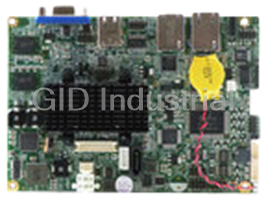
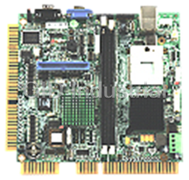
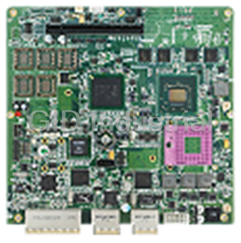
ACROSSER AR-B1322
Description
PC/104 386SX CPU BOARD
Part Number
AR-B1322
Price
Request Quote
Manufacturer
ACROSSER
Lead Time
Request Quote
Category
Single Board Computers
Specifications
System Chipset
ALi M6117C
Form Factor
PC/104 Standard
Ethernet Chipset
Novell NE2000
BIOS
AMI flash BIOS
Bus Interface
Stack-through PC/104 bus
Bus Speed
7.159MHz (default)
CPU & Chipset
ALI M6117C, 25/33/40 MHz (33 MHz as standard)
Dimensions
90.2mmX95.9mm (3.55”X3.775”)
DMA Channels
7 DMA channels
DRAM
Up to 4MB with 2 MB on-board
Ethernet
10 Base-T NE2000 compatible with 7-pin 2.5mm JST connector
Flash Disk
Supports vertical or horizontal- type 44-pin DiskOnModule
Floppy
One floppy drive with a 6-pin 2.0mm connector
Humidity
0 to 95% (non-condensing)
IDE
One 44-pin 2.0 mm connector supports 2 IDE drives
Interrupt Levels
15 vectored interrupt levels
Keyboard & Mouse
PS/2 compatible with 6-pin 2.0mm JST connector
LED Indicator
Power LED
Operating Temp.
0 to 60° C (140° F)
Parallel Port
Support 1 SPP/EPP/ECP mode printer port with the 26-pin 2.0mm connector
PC Board
6 layers
Power Connector
4-pin (2.5mm) power connector (+5V, GND, GND, +12V)
Power Req.
+5V only, 1.0A maximum (Based on 33 MHz CPU)
Real Time Clock
M48T86PC1 or compatible chips
Serial Port
2 full RS-232C ports with 10-pin header, or 2 RS-485 ports for twisted pair multi-drop use
Speaker
External speaker with one 2-pin header
Storage Temp.
-25 to 85° C
Watchdog
Programmable watchdog timer
Weight
120g
Features
- 80386SX-33/40 MHz CPU (on-board 33 MHz CPU as standard model)
- Dimensions: 90.2mmX95.9mm (3.55”x3.775”)
- Flash BIOS
- Multi-layer PCB for noise reduction
- Powered-on LED indicator
- Programmable watchdog timer
- PS/2 compatible keyboard interface
- Signal 5V power requirement
- Stack-through PC/104 extension bus
- Supports 10 Base-T NE2000 compatible with 7-pin 2.5mm JST connector
- Supports 2 RS-232C/RS-485 serial ports
- Supports DiskOnModule flash disk
- Supports one floppy drive
- Supports one SPP/EPP/ECP printer port
- Supports two IDE drives
- System of up to 4MB DRAM (2 MB already on-board)
Datasheet

Extracted Text
AR-B1322
PC/104 386SX CPU BOARD
User’s Guide
Edition: 1.2
Book Number: AR-B1322-99.A01
A AR R- -B B1 13 32 22 2
Copyright Notice and Disclaimer
October 1999
Acrosser Technology makes no representations or warranties with respect to the contents hereof and
specifically disclaims any implied warranties of merchantability or fitness for any particular purpose.
Furthermore, Acrosser Technology reserves the right to revise this publication and to make changes from
time to time in the contents hereof without obligation of Acrosser Technology to notify any person of such
revisions or changes. Check for updates at www.acrosser.com
Possession, use, or copying of the software described in this publication is authorized only pursuant to a
valid written license from Acrosser or an authorized sublicensor.
(C) Copyright 錯誤 錯誤! 尚未定義書籤。 尚未定義書籤。 Acrosser Technology Co., Ltd., 1999. All rights Reserved.
錯誤 錯誤 尚未定義書籤。 尚未定義書籤。
Acrosser, Intel, ALI, AMI…are registered trademarks.
All other trademarks and registered trademarks are the property of their respective holders.
This document was produced with Adobe Acrobat 3.01.
II
A AR R- -B B1 13 32 22 2
Table of Contents
0. PREFACE .............................................................................................................................................V
0.1 WELCOME TO THE AR-B1322 CPU BOARD ............................................................................................ V
0.2 BEFORE YOU USE THIS GUIDE................................................................................................................. V
0.3 RETURNING YOUR BOARD FOR SERVICE............................................................................................. V
0.4 TECHNICAL SUPPORT AND USER COMMENTS.................................................................................... V
0.5 ORGANIZATION..........................................................................................................................................VI
0.6 STATIC ELECTRICITY PRECAUTIONS ...................................................................................................VI
1. OVERVIEW........................................................................................................................................ 1-1
1.1 INTRODUCTION.........................................................................................................................................1-1
1.2 PACKING LIST............................................................................................................................................1-1
1.3 FEATURES...................................................................................................................................................1-2
2. SYSTEM CONTROLLER ................................................................................................................ 2-1
2.1 MICROPROCESSOR...................................................................................................................................2-1
2.2 DMA CONTROLLER...................................................................................................................................2-1
2.3 DRAM CONFIGURATION..........................................................................................................................2-2
2.4 I/O CONTROLLER.......................................................................................................................................2-2
2.5 I/O PORT ADDRESS MAP ..........................................................................................................................2-3
2.6 INTERRUPT CONTROLLER......................................................................................................................2-4
2.7 SERIAL PORTS............................................................................................................................................2-5
2.8 PARALLEL PORT........................................................................................................................................2-7
2.9 TIMER...........................................................................................................................................................2-9
2.10 REAL-TIME CLOCK AND NON-VOLATILE RAM .................................................................................2-9
2.11 WATCHDOG TIMER.................................................................................................................................2-10
2.12 FLASH DISK..............................................................................................................................................2-10
2.13 ETHERNET CONTROLLER.....................................................................................................................2-10
3. SETTING UP THE SYSTEM........................................................................................................... 3-1
3.1 BOARD LAYOUT........................................................................................................................................3-2
3.2 CPU BASE CLOCK SELECT (JP1).............................................................................................................3-4
3.3 SWITCH SETTINGS (SW1).........................................................................................................................3-4
3.4 ETHERNET CONNECTOR(J1)...................................................................................................................3-5
EXTERNAL LED HEADER (J2) ............................................................................................................................3-5
3.6 KEYBOARD CONNECTOR (J3).................................................................................................................3-5
3.7 RESET HEADER (J4)...................................................................................................................................3-5
3.8 SPEAKER HEADER (J5) .............................................................................................................................3-6
3.9 POWER CONNECTOR (J6).........................................................................................................................3-6
3.10 PRINTER CONNECTOR (CN1) ..................................................................................................................3-6
3.11 FLOPPY CONNECTOR (CN2)....................................................................................................................3-7
3.12 SERIAL PORT CONNECTORS (CN3, CN4 & CN5) .................................................................................3-8
3.12.1 RS-232C CONNECTORS (CN3 & CN4) ................................................................................................................3-8
3.12.2 RS-485 CONNECTOR (CN5) .................................................................................................................................3-9
3.12.3 RS-485 TERMINATOR (JP2 & JP3) ......................................................................................................................3-9
3.13 HARD DISK CONTROLLER (CN6) .........................................................................................................3-10
3.14 PC/104 CONNECTOR (CN7 & CN8) ........................................................................................................3-11
3.14.1 64 PIN PC/104 CONNECTOR – CN8 (BUS A & B).............................................................................................3-11
3.14.2 40 PIN PC/104 CONNECTOR - CN7 (BUS C & D).............................................................................................3-12
3.14.3 PC/104 CHANNEL SIGNAL DESCRIPTION.......................................................................................................3-13
3.15 LED INDICATOR (LED1 & LED2) ..........................................................................................................3-14
3.15.1 POWER LED (LED1) ...........................................................................................................................................3-14
3.15.2 STATUS LED (LED2)...........................................................................................................................................3-14
3.16 DISKONMODULE.....................................................................................................................................3-15
III
A AR R- -B B1 13 32 22 2
4. BIOS CONSOLE............................................................................................................................... 4-1
4.1 BIOS SETUP OVERVIEW...........................................................................................................................4-1
4.2 STANDARD CMOS SETUP ........................................................................................................................4-2
4.3 ADVANCED CMOS SETUP .......................................................................................................................4-4
4.4 ADVANCED CHIPSET SETUP...................................................................................................................4-7
4.5 PERIPHERAL SETUP..................................................................................................................................4-9
4.6 AUTO-DETECT HARD DISKS.................................................................................................................4-10
4.7 PASSWORD SETTING..............................................................................................................................4-10
4.8 SETTING THE PASSWORD .....................................................................................................................4-10
4.8.1 CHECKING THE PASSWORD.............................................................................................................................4-11
4.9 LOAD THE DEFAULT SETTING.............................................................................................................4-11
4.9.1 AUTO CONFIGURATION WITH OPTIMAL SETTING.......................................................................................4-11
4.9.2 AUTO CONFIGURATION WITH FAIL SAFE SETTING.....................................................................................4-11
4.10 BIOS EXIT..................................................................................................................................................4-11
4.10.1 SAVE SETTINGS AND EXIT ................................................................................................................................4-11
4.10.2 EXIT WITHOUT SAVING.....................................................................................................................................4-12
4.11 BIOS UPDATE...........................................................................................................................................4-12
5. SYSTEM INSTALLATION............................................................................................................... 5-1
5.1 OVERVIEW..................................................................................................................................................5-1
5.2 UTILITY DISKETTE...................................................................................................................................5-1
5.2.1 NETWORK UTILITY..............................................................................................................................................5-2
5.2.2 WATCHDOG TIMER..............................................................................................................................................5-2
5.2.2.1 WATCHDOG TIMER SETTING .....................................................................................................5-2
5.2.2.2 WD ENABLE REGISTER - INDEX 37H ........................................................................................5-3
5.2.2.3 WD REPORT REGISTER - INDEX 38H.........................................................................................5-3
5.2.2.4 WD TIMER COUNTER(24 BITS) - INDEX 39H, 3AH, AND 3BH...............................................5-3
5.2.2.5 TIMEOUT STATUS & RESET WATCHDOG - INDEX 3CH........................................................5-4
5.2.2.6 PROGRAMMING WATCHDOG - BASIC OPERATION ..............................................................5-4
A. APPENDIX........................................................................................................................................ A-1
A-1 SPECIFICATIONS......................................................................................................................................A-1
A-2 BOARD DIMENSIONS..............................................................................................................................A-2
A-3 PROGRAMMING THE RS-485 .................................................................................................................A-3
IV
A AR R- -B B1 13 32 22 2
0. PREFACE
0.1 WELCOME TO THE AR-B1322 CPU BOARD
This guide introduces the Acrosser AR-B1322 CPU board.
This guide describes this card’s functions, features, and how to start, set up and operate your AR-
B1322. You could also find the general system information here.
0.2 BEFORE YOU USE THIS GUIDE
If you have not already installed this AR-B1322, refer to Chapter 3, “Setting System,” in this guide.
0.3 RETURNING YOUR BOARD FOR SERVICE
If your board requires servicing, contact the dealer from whom you purchased the product for
service information. If you need to ship your board to us for service, be sure it is packed in a
protective carton. We recommend that you keep the original shipping container for this purpose.
You can help assure efficient servicing of your product by following these guidelines:
1). Include your name, address, daytime telephone, facsimile number and e-mail where you may
be reached
2). A description of the system configurations and/or the software at the time of malfunction.
3). A brief description of the symptoms.
0.4 TECHNICAL SUPPORT AND USER COMMENTS
User's comments are always welcome as they assist us in improving the usefulness of our products
and the understanding of our publications. They form a very important part of the input used for
product enhancement and revision.
We may use and distribute any of the information you supply in any way we believe appropriate
without incurring any obligation. You may, of course, continue to use the information you supply.
If you have suggestions for improving particular sections or if you find any errors, please indicate
the manual title and book number.
Please send your comments to Acrosser Technology Co., Ltd. or your local sales representative.
Send Internet electronic mail to: Sales@acrosser.com
V
A AR R- -B B1 13 32 22 2
0.5 ORGANIZATION
This information covers the following topics (see the Table of Contents for a detailed listing):
� Chapter 1, “Overview,” provides an overview of the system features and packing list.
� Chapter 2, “System Controller,” describes the major structure.
� Chapter 3, “Setting the System,” describes how to adjust the jumpers, and the connector
settings.
� Chapter 4, “BIOS Console,” providing the BIOS settings.
� Chapter 5, “System Installation,” providing hardware and driver installing procedures
� Appendix
� Specifications
� Board dimensions
� Programming the RS-485
0.6 STATIC ELECTRICITY PRECAUTIONS
Before removing the board from its anti-static bag, read this section about the static electricity
precautions.
Static electricity is a constant danger to computer systems. The charge that can build up in your
body may be more than sufficient to damage integrated circuits on any PC board. It is, therefore,
important to observe basic precautions whenever you use or handle computer components.
Although areas with humid climates are much less prone to the static built up, it is always best to
safeguard against accidents, which may result in expensive repairs. The following measures
should generally be sufficient to protect your equipment from static discharge:
1) Touch a grounded metal object to discharge the static electricity in your body (or ideally,
wear a grounded wrist strap).
2) When unpacking and handling the board or other system components, place all materials
on an antic-static surface.
3) Be careful not to touch the components on the board, especially the “gold finger”
4) connectors on the bottom of every board.
VI
A AR R- -B B1 13 32 22 2
1. OVERVIEW
This chapter provides an overview of your system features and capabilities. The following topics
are covered:
� Introduction
� Packing List
� Features
1.1 INTRODUCTION
The AR-B1322, PC/104 CPU module is a lower power consuming, high performance 386 based
computer. By using the space-saving features of the ALI M6117C CPU, this module is able to
support up to 4MB of DRAM. The unit also comes with two RS-232C/RS-485 ports, 1 parallel port,
1 floppy interface, 1 IDE interface, and 1 DiskOnChip socket for adding a high degree of versatility
to any project. The AR-B1322 is an excellent choice for mobile systems, or as a controller for
machines that are too small to accommodate traditional industrial PCs.
The AR-B1322 offers higher speed and it makes a very stable 386SX-based system with a true
PC/104 module for embedded applications. It also has LAN onboard with support of 10 Mbps
transmission rate. Acrosser additionally provides AR-B9450 ethernet adapter module to ensure
efficient LAN applictions.
This manual has been written to assist you in installing, configuring and running the AR-B1322
CPU card. Each section is intended to guide you through its procedures clearly and concisely,
allowing you to continue to the next chapters without any difficulty.
1.2 PACKING LIST
These accessories are included with the system. Before you begin installing your AR-B1322
board, take a moment to make sure that the following items have been included inside the AR-
B1322 package.
� A quick setup guide
� 1 AR-B1322 PC/104 386SX CPU board
� 1 Keyboard adapter cable
� 1 Floppy adapter cable
� 2 RS-232C interface cables
� 1 Printer adapter cable
� 1 Power adapter cable
� 1 Utility diskette
� 1 LAN adapter cable
Accessory Description
Keyboard adapter cable 6-pin JST to 6-pin mini-din IBM PS/2 standard type
Floppy adapter cable 16-pin mini-IDC to 34-pin IDC
RS-232C interface cable 10-pin IDC to DB-9 male
Printer adapter cable 26-pin mini-IDC to DB-25 female
Power adapter cable 4-pin JST power cable
LAN adapter cable Acrosser’s AR-B9450 RJ-45 adapter module with 2 LED indicators
(about 15mm in length)
Table 1-1 Accessories
1-1
A AR R- -B B1 13 32 22 2
1.3 FEATURES
This system provides a number of special features that enhance its reliability, ensure its
availability, and improve its expansion capabilities, as well as its hardware structure.
� 80386SX-33/40 MHz CPU (on-board 33 MHz CPU as standard model)
� Stack-through PC/104 extension bus
� System of up to 4MB DRAM (2 MB already on-board)
� Supports 2 RS-232C/RS-485 serial ports
� PS/2 compatible keyboard interface
� Programmable watchdog timer
� Flash BIOS
� Supports two IDE drives
� Supports 10 Base-T NE2000 compatible with 7-pin 2.5mm JST connector
� Supports one floppy drive
� Supports one SPP/EPP/ECP printer port
� Supports DiskOnModule flash disk
� Powered-on LED indicator
� Signal 5V power requirement
� Multi-layer PCB for noise reduction
� Dimensions: 90.2mmX95.9mm (3.55”x3.775”)
1-2
A AR R- -B B1 13 32 22 2
2. SYSTEM CONTROLLER
This chapter describes the major structure. The following topics are covered:
� Microprocessor
� DMA Controller
� DRAM Configuration
� I/O Port Address Map
� Interrupt Controller
� Serial Port
� Parallel Port
� Timer
� Real-Time Clock and Non-Volatile RAM
� Watch-Dog Timer
� FLASH Disk
� Ethernet controller
2.1 MICROPROCESSOR
The AR-B1322 uses the ALI M6117C CPU; it is designed to perform like Intel’s 386SX-based
system with deep green features.
The 386SX core is the same as M1386SX of Acer Labs. Inc. and 100% object code compatible
with the Intel 386SX microprocessor. System manufacturers can provide 386 CPU based
systems optimized for both cost and size. Instruction pipelining and high bus bandwidth ensure
short average instruction-execution times and high system throughput. Furthermore, it can keep
the state internally from charge leakage while external clock to the core is stopped without storing
the data in registers. The power consumption here is almost zero when the clock stops. The
internal structure of this core is 32-bit and it’s address bus has a very low supply current. The real
mode as well as the protected mode are available and can run MS-DOS, MS-Windows, OS/2 and
UNIX.
2.2 DMA CONTROLLER
The equivalent of two 8237A DMA controllers are implemented in the AR-B1322 card. Each
controller is a four-channel DMA device, which will generate the memory addresses and control
signals necessary to transfer information directly between a peripheral device and memory. This
allows high-speed information transfer with less CPU intervention. The two DMA controllers are
internally cascaded to provide four DMA channels for transfers to 8-bit peripherals (DMA1) and
three channels for transfers to 16-bit peripherals (DMA2). DMA2 channel 0 provides the cascade
interconnection between the two DMA devices, thereby maintaining the IBM PC/AT compatibility.
The following is the DMA channels:
DMA Controller 1 DMA Controller 2
Channel 0: Spare Channel 4: Cascade for controller 1
Channel 1: IBM SDLC Channel 5: Spare
Channel 2: Diskette adapter Channel 6: Spare
Channel 3: Spare Channel 7: Spare
Table 2-1 DMA Channel Controller
2-1
A AR R- -B B1 13 32 22 2
2.3 DRAM CONFIGURATION
There are two 16-bit memory banks on the AR-B1322 board. The first bank is embedded with a 1MBx16-bit
(2MB, 60ns) EDO RAM and the other is 42-pin SOJ socket for extra 2MB DRAM with 1MBx16-bit (2MB,
60ns) EDO RAM. Please refer to the following table for details:
U15 (On-Board) U1 (Socket) Total Memory Remark
EDO 1Mx16 None 2MB Factory Preset
EDO 1Mx16 EDO 1Mx16 4MB
Table 2-2 DRAM Configuration
2.4 I/O CONTROLLER
A super I/O chip (SMC37C669) is embedded at the back panel of the AR-B1322 board. It combines the
functions of a floppy disk drive adapter, a hard disk drive (IDE) adapter, two serial (with 16C550 UART)
adapters and 1 parallel adapter. Setting the BIOS setup program can do the I/O port configurations.
As a UART, the chip supports the serial to parallel conversion on data characters received from a peripheral
device or a MODEM, and the parallel to serial conversion on data character received from the CPU. The
UART includes a programmable baud rate generator, complete MODEM control capability and a processor
interrupt system. For the parallel port, the SMC37C669 provides the user with a fully bi-directional
centronics-type printer interface.
2-2
A AR R- -B B1 13 32 22 2
2.5 I/O PORT ADDRESS MAP
Hex Range Device Factory Preset
000-01F DMA controller 1
020-021 Interrupt controller 1
022-023 ALI M6117C chipset address
040-04F Timer 1
050-05F Timer 2
060-06F 8042 keyboard/controller
070-071 Real-time clock (RTC), non-maskable interrupt
(NMI)
080-09F DMA page registers
0A0-0A1 Interrupt controller 2
0C0-0DF DMA controller 2
0F0 Clear Math Co-processor
0F1 Reset Math Co-processor
0F8-0FF Math Co-processor
170-178 Fixed disk 1
1F0-1F8 Fixed disk 0
201 Game port
208-20A EMS register 0
218-21A EMS register 1
278-27F Parallel printer port 3 (LPT 3)
2E8-2EF Serial port 4 (COM 4)
2F8-2FF Serial port 2 (COM 2)
300-31F Ethernet controller
378-37F Parallel printer port 2 (LPT 2)
380-38F SDLC, bisynchronous
3A0-3AF Bisynchronous
3B0-3BF Monochrome display and printer port 1 (LPT 1)
3C0-3CF EGA/VGA adapter
3D0-3DF Color/Graphics monitor adapter
3E8-3EF Serial port 3 (COM 3)
3F0-3F7 Floppy controller
3F8-3FF Serial port 1 (COM 1)
Table 2-3 I/O Port Address Map
Note: The I/O port address with the mark “” is factory preset value and is not adjustable. The
items marked “” can be adjusted in BIOS setup.
2-3
A AR R- -B B1 13 32 22 2
2.6 INTERRUPT CONTROLLER
The ALI M6117C also provides two cascaded 8259 Programmable Interrupt Controllers (PIC). They
accept requests from the peripherals, resolve priorities on pending interrupts in service, issue
interrupt requests to the CPU, and provide vectors which are used as acceptance indexed by the
CPU to determine which interrupt service routine should be executed.
The following is the system information of interrupt levels:
Description
In Interrupt Level
Parity check
NMI
CTRL2
CTRL1
System timer interrupt from timer 8254
IRQ 0
IRQ 1
Keyboard output buffer full
IRQ 2
: Real time clock
IRQ8
: Rerouting to INT 0Ah from hardware IRQ2
IRQ9
: LAN
IRQ10
IRQ11 : Spare
IRQ12 : Spare
IRQ13 : Reserved for Math. coprocessor
: Hard disk adapter
IRQ14
IRQ15 : Spare
IRQ 3 Serial port 2
IRQ 4 Serial port 1
Spare
IRQ 5
IRQ 6 Floppy disk
IRQ 7
Parallel port
d4
Figure 2-1 Interrupt Controller
2-4
A AR R- -B B1 13 32 22 2
2.7 SERIAL PORTS
The ACEs (Asynchronous Communication Elements ACE1 and ACE2) are used to convert the
parallel data to a serial format on the transmit side and convert the serial data to parallel on the
receiver side. The serial format, in order of transmission and reception, is a start bit, followed by
five to eight data bits, a parity bit (if programmed) and one, one and half (five-bit format only) or
two stop bits. The ACEs are capable of handling divisors of 1 to 65535, and produce a 16x clock
for driving the internal transmitter logic.
Provisions are also included to use this 16x clock to drive the receiver logic. Also included in the
ACE are a complete MODEM control capability, and a processor interrupt system that may be
software tailored to the computing time required to handle the communications link. The following
is a summary of each ACE accessible registers.
DLAB Port Address Register
0 base + 0 Receiver buffer (RBR, read)
Transmitter holding register (THR, write)
0 base + 1 Interrupt enable (IER)
X base + 2 Interrupt identification (IIR, read only)
X base + 3 Line control (LCR)
X base + 4 MODEM control (MCR)
X base + 5 Line status (LSR)
X base + 6 MODEM status (MSR)
X base + 7 Scratched register
1 base + 0 Divisor latch (least significant byte) (LS)
1 base + 1 Divisor latch (most significant byte) (MS)
Table 2-4 ACE Accessible Register
(1) Receiver Buffer Register (RBR)
Bit 0-7: Received data byte (Read Only)
(2) TRANSMITTER HOLDING REGISTER (THR)
Bit 0-7: Transmitter holding data byte (Write Only)
(3) INTERRUPT ENABLE REGISTER (IER)
Bit 0: Enable Received Data Available Interrupt (ERBFI)
Bit 1: Enable Transmitter Holding Empty Interrupt (ETBEI)
Bit 2: Enable Receiver Line Status Interrupt (ELSI)
Bit 3: Enable MODEM Status Interrupt (EDSSI)
Bit 4: Must be 0
Bit 5: Must be 0
Bit 6: Must be 0
Bit 7: Must be 0
(4) INTERRUPT IDENTIFICATION REGISTER (IIR)
Bit 0: “0” if Interrupt Pending
Bit 1: Interrupt ID Bit 0
Bit 2: Interrupt ID Bit 1
Bit 3: Must be 0
Bit 4: Must be 0
Bit 5: Must be 0
Bit 6: Must be 0
Bit 7: Must be 0
2-5
A AR R- -B B1 13 32 22 2
(5) LINE CONTROL REGISTER (LCR)
Bit 0: Word Length Select Bit 0 (WLS0)
Bit 1: Word Length Select Bit 1 (WLS1)
WLS1 WLS0 Word Length
0 0 5 Bits
0 1 6 Bits
1 0 7 Bits
1 1 8 Bits
Bit 2: Number of Stop Bit (STB)
Bit 3: Parity Enable (PEN)
Bit 4: Even Parity Select (EPS)
Bit 5: Stick Parity
Bit 6: Set Break
Bit 7: Divisor Latch Access Bit (DLAB)
(6) MODEM CONTROL REGISTER (MCR)
Bit 0: Data Terminal Ready (DTR)
Bit 1: Request to Send (RTS)
Bit 2: Out 1 (OUT 1)
Bit 3: Out 2 (OUT 2)
Bit 4: Loop
Bit 5: Must be 0
Bit 6: Must be 0
Bit 7: Must be 0
(7) LINE STATUS REGISTER (LSR)
Bit 0: Data Ready (DR)
Bit 1: Overrun Error (OR)
Bit 2: Parity Error (PE)
Bit 3: Framing Error (FE)
Bit 4: Break Interrupt (BI)
Bit 5: Transmitter Holding Register Empty (THRE)
Bit 6: Transmitter Shift Register Empty (TSRE)
Bit 7: Must be 0
(8) MODEM STATUS REGISTER (MSR)
Bit 0: Delta Clear to Send (DCTS)
Bit 1: Delta Data Set Ready (DDSR)
Bit 2: Training Edge Ring Indicator (TERI)
Bit 3: Delta Receive Line Signal Detect (DSLSD)
Bit 4: Clear to Send (CTS)
Bit 5: Data Set Ready (DSR)
Bit 6: Ring Indicator (RI)
Bit 7: Received Line Signal Detect (RSLD)
2-6
A AR R- -B B1 13 32 22 2
(9) DIVISOR LATCH (LS, MS)
Byte Data LS MS
Bit 0: Bit 0 Bit 8
Bit 1: Bit 1 Bit 9
Bit 2: Bit 2 Bit 10
Bit 3: Bit 3 Bit 11
Bit 4: Bit 4 Bit 12
Bit 5: Bit 5 Bit 13
Bit 6: Bit 6 Bit 14
Bit 7: Bit 7 Bit 15
Desired Divisor Used to Present Error Difference
Baud Rate Generate 16x Clock Between Desired and Actual
50 2304 ---
75 1536 ---
110 1047 0.026
134.5 857 0.058
150 768 ---
300 384 ---
600 192 ---
1200 96 ---
1800 64 ---
2000 58 0.69
2400 48 ---
3600 32 ---
4800 24 ---
7200 16 ---
9600 12 ---
14400 8 ---
19200 6 ---
28800 4 ---
38400 3 ---
57600 2 ---
115200 1 ---
Table 2-5 Serial Port Divisor Latch
2.8 PARALLEL PORT
(1) Register Address
Port Address Read/Write Register
base+0 Write Output data
base+0 Read Input data
base+1 Read Printer status buffer
base+2 Write Printer control latch
Table 2-6 Parallel Port Register
(2) Printer Interface Logic
The parallel portion of the SMC37C669 makes the attachment of various devices that accept eight bits
of parallel data at standard TTL level.
2-7
A AR R- -B B1 13 32 22 2
(3) Data Swapper
The system microprocessor can read the contents of the printer's Data Latch through the Data Swapper
by reading the Data Swapper address.
(4) Printer Status Buffer
The system microprocessor can read the printer status by reading the address of the Printer Status
Buffer. The bit definitions are described as follows:
70 6 5 4 3 2 1
XXX
-ERROR
SLCT
PE
-ACK
-BUSY
Bit 7: This signal may become active during data entry, when the printer is off-line during printing, or
when the print head is changing position or in an error state. When Bit 7 is active, the printer is
busy and can not accept data.
Bit 6: This bit represents the current state of the printer's ACK signal. A 0 means the printer has
received the character and is ready to accept another. Normally, this signal will be active for
approximately 5 microseconds before BUSY stops.
Bit 5: A 1 means the printer has detected the end of paper.
Bit 4: A 1 means the printer is selected.
Bit 3: A 0 means the printer has encountered an error condition.
Bit 0-2: No meaning.
(5) Printer Control Latch & Printer Control Swapper
The system microprocessor can read the contents of the printer control latch by reading the address of
printer control swapper. Bit definitions are as follows:
70 6 5 4 3 2 1
XX
STROBE
AUTO FD XT
INIT
SLDC IN
IRQ ENABLE
DIR(write only)
Bit 5: Direction control bit. When logic 1, the output buffers in the parallel port are disabled
allowing data driven from external sources to be read; when logic 0, they work as a
printer port. This bit is write only.
Bit 4: A 1 in this position allows an interrupt to occur when ACK changes from low state to
high state.
Bit 3: A 1 in this bit position selects the printer.
Bit 2: A 0 starts the printer (50μsecond pulse, minimum).
Bit 1: A 1 causes the printer to line-feed after a line is printed.
Bit 0: A 0.5μsecond minimum high active pulse clocks data into the printer. Valid data must
be present for a minimum of 0.5μseconds before and after the strobe pulse.
2-8
A AR R- -B B1 13 32 22 2
2.9 TIMER
The AR-B1322 provides three programmable timers, each with a timing frequency of 1.19 MHz.
Timer 0 The output of this timer is tied to interrupt request 0. (IRQ 0)
Timer 1 This timer is used to trigger memory refresh cycles.
Timer 2 This timer provides the speaker tone.
Application programs can load different counts into this timer to
generate various sound frequencies.
Table 2-7 Timer
2.10 REAL-TIME CLOCK AND NON-VOLATILE RAM
The AR-B1322 contains a real-time clock compartment that maintains the date and time in
addition to storing configuration information about the computer system. It contains 14 bytes of
clock and registers and 114 bytes of general purpose RAM. Because of the use of CMOS
technology, it consumes very little power and can be maintained for long periods of time using an
internal lithium battery.
Address Description
00 Seconds
01 Second alarm
02 Minutes
03 Minute alarm
04 Hours
05 Hour alarm
06 Day of week
07 Date of month
08 Month
09 Year
0A Status register A
0B Status register B
0C Status register C
0D Status register D
0E Diagnostic status byte
0F Shutdown status byte
10 Diskette drive type byte, drive A and B
11 Fixed disk type byte, drive C
12 Fixed disk type byte, drive D
13 Reserved
14 Equipment byte
15 Low base memory byte
16 High base memory byte
17 Low expansion memory byte
18 High expansion memory byte
19-2D Reserved
2E-2F 2-byte CMOS checksum
30 Low actual expansion memory byte
31 High actual expansion memory byte
32 Date century byte
33 Information flags (set during power on)
34-7F Reserved for system BIOS
Table 2-8 Real-Time Clock & Non-Volatile RAM
2-9
A AR R- -B B1 13 32 22 2
2.11 WATCHDOG TIMER
The AR-B1322 is equipped with a programmable time-out period watchdog timer. Actually, the
watchdog timer is provided by the ALI M6117C chipset. You can use the program to enable the
watchdog timer. Once you have enabled the watchdog timer, the program should trigger it every
time before it times out. If your program fails to trigger or disable this timer before it times out
because of a system hang-up, it will generate a reset signal to reset the system or trigger an IRQ
or NMI signal to tell your program that the watchdog has timed out. The time-out period can be
programmed to be from 30.5μseconds to 512 seconds with 30.5μseconds per step.
2.12 FLASH DISK
The AR-B1322 supports DiskOnModule flash disk, which makes it ideal for diskless systems, and
are also highly reliable for high-speed access applications, such as controllers for industrial use,
line test instruments, etc.
2.13 ETHERNET CONTROLLER
The Ethernet controller of the AR-B1322 is a highly integrated design that provides all Media
Access Control (MAC) and Encode-Decode (ENDEC) functions in accordance with the IEEE
802.3 standard. The Ethernet controller can interface directly with the PC-AT ISA bus without any
external device. The interface to PC-AT ISA bus is fully compatible with NE2000 Ethernet adapter
cards, so all software programs designed for NE2000 standard can run on the Ethernet controller
card without any modification.
Microsoft’s Plug and Play and the jumperless software configuration function are both supported.
The capability of the PnP and Non-PnP mode autoswitch function allows the users to configure
network card. No jumpers or switches are needed to set additionally when using either the PC or
PnP function. The integrated 8Kx16 SRAM and 10BASE-T transceiver make Ethernet controller
more cost-effective.
2-10
A AR R- -B B1 13 32 22 2
3. SETTING UP THE SYSTEM
This section describes the pin assignments of all connectors and settings of all switches and
jumpers. It also guides you on how to expand the system and control the onboard devices.
The jumper pins allow you to set specific system parameters. Set them by changing the pin
location of jumper blocks. (A jumper block is a small plastic-encased conductor that slips over the
pins.) To change a jumper setting, remove the jumper from its current location with your fingers or small
needle-nosed pliers. Place the jumper over the two pins designated for the desired setting. Press
the jumper evenly onto the pins. Be careful not to bend the pins.
We will show the locations of the AR-B1322 jumper pins, and the factory-default settings in this
section. Note that the square pin of each jumper block is pin 1.
Below illustrates the jumper use. Jumper caps are usually small plastic caps used to short two
pins on a jumper block.
Most jumper caps look like this:
A Jumper
Cap
Most jumper blocks look like this:
A 3 Pin jumper
Block
If the jumper is placed over pins one and two then 1-2 are ON.
Jumper on
Pins1 + 2
If the jumper is placed over pins two and three then 2-3 are ON.
Jumper On
Pins 2 + 3
Otherwise, the jumper can be left to the side or completely off the block to keep both 1-2 and 2-3
off (open).
CAUTION: Do not touch any electronic component unless you are safely grounded. Wear a grounded
wrist strap or touch an exposed metal part of the system unit chassis. Static discharges from
your fingers can permanently damage electronic components.
3-1
A AR R- -B B1 13 32 22 2
3.1 BOARD LAYOUT
The AR-B1322 is a small, easy to use, all-in-one 386SX grade CPU board with two RS-232/RS-
485 ports and a flash disk module. Below is the AR-B1322 board layout.
CN3
JP1
CN4
JP2
JP3
CN5
J2
J4
J5
J6
Figure 3-1 AR-B1322 Board Layout
3-2
A AR R- -B B1 13 32 22 2
Name Function Section
JP1 CPU base clock select 3.2
JP2 RS-485 terminator select (COM-A) 3.12.3
JP3 RS-485 terminator select (COM-B) 3.12.3
SW1 Switch 1 COM-A port mode selector 3.3
Switch 2 COM-B port mode selector 3.3
J1 Ethernet connector 3.4
J2 External power and hard disk LED header 3.5
J3 PS/2 Keyboard connector 3.6
J4 Reset header 3.7
J5 Speaker header 3.8
J6 Power connector 3.9
CN1 Printer connector 3.10
CN2 Floppy connector 3.11
CN3 RS-232C connector (COM-A) 3.12.1
CN4 RS-232C connector (COM-B) 3.12.1
CN5 RS-485 connector 3.12.2
CN6 44-pin IDE connector 3.13
CN7 40-pin PC/104 connector (Bus C & D) 3.14.2
CN8 64-pin PC/104 connector (Bus A & B) 3.14.1
LED1 Onboard power LED 3.15.1
LED2 User defined status LED 3.15.2
U1 Expandable DRAM socket 2.3
Table 3-1 Important Component List
3-3
A AR R- -B B1 13 32 22 2
3.2 CPU BASE CLOCK SELECT (JP1)
This board provides six types of CPU input clocks; they are 33.3MHz, 50MHz, 60MHz, 66.7MHz,
75MHz, and 80MHz. The CPU input clock is twice that of the operating clock. JP1 is a 6-pin
jumper located between CN3 and CN4.
CPU Input Clock CPU Operating Clock JP1 Setting Remark
33.3MHz 16.7MHz Short 1-2 & 4-6
50MHz 25MHz Short 1-2 & 3-5
60MHz 30MHz Short 1-2 & 5-6
66.7MHz 33.3MHz Short 1-3 & 5-6 Factory Preset
75MHz 37.5MHz Short 2-4 & 5-6
80MHz 40MHz Short 1-3 & 2-4
Table 3-2 CPU Clock Settings
JP1 JP1 JP1 JP1 JP1 JP1
1 � 21 � 21 � 21 � 21 � 21 � 2❏❏❏❏❏❏
3 43 43 43 43 43 4
�� �� �� �� �� ��
5 65 65 65 65 65 6
�� �� �� �� �� ��
16.7 MHz 25 MHz 30 MHz 33.3 MHz 37.5 MHz 40 MHz
Figure 3-2 JP1: CPU Clock Select
3.3 SWITCH SETTINGS (SW1)
SW1 is a DIP switch. It provides multi-purpose selection in one switch. The following table gives the details:
ON
1 2
SW1 Function When “OFF” When “ON” Factory Preset
Switch 1 COM-A port mode select RS-232C RS-485 Off
Switch 2 COM-B port mode select RS-232C RS-485 Off
Table 3-3 SW1 Settings
Note: When set to RS-485, the Acrosser RS-485 adapter must be used in conjunction for the RS-485 to work.
3-4
A AR R- -B B1 13 32 22 2
3.4 ETHERNET CONNECTOR(J1)
This system has ethernet onboard. Install the network driver from the utility diskette, and connect
the Acrosser AR-B9450 ethernet adapter module to J1. The included ethernet module AR-B9450
is specially designed for the network applications. It has two LED indicators: yellow and green.
When the system is receiving/transmitting data, the yellow LED blinks to show the system is
working. The green LED is reserved for future purposes.
� 7 LANLED-
� 6 LANLED+
J1
AR-B9450
� 5 Ground
� 4 TPRX-
3 TPRX+
�
2 TPTX-
�
1 TPTX+❏
Figure 3-3 Ethernet Connector Pin Assignments and AR-B9450 Ethernet Adapter Module
3.5 EXTERNAL LED HEADER (J2)
The J2 is a 4-pin right angle header. It allows you to connect an external power LED and an external hard
disk LED.
121 POWER LED+
� � 2 HARD DISK LED+
❏� 3 POWER LED-
3 4 4 HARD DISK LED-
Figure 3-4 J2: External LED Header
3.6 KEYBOARD CONNECTOR (J3)
The J3 is a 6-pin 2.0mm JST connector. Use the keyboard adapter cable to connect a PS/2 type
keyboard. The following figure shows the adapter cable’s pin assignment.
6 Pin Mini-Din
1 1 DATA
Reserved❏
1 2
2
KB Data �
2 N.C.
3 4
3 �
GND
3 GND
4 �
VCC
4 VCC
5 6
5
Reserved �
5 CLOCK
6 �
KB Clock
6 N.C.
Figure 3-5 J3: Keyboard Connector
3.7 RESET HEADER (J4)
The J4 is used to connect to an external reset switch. Shorting these two pins will reset the
system.
12 1 Reset+
J4: Reset
2 Reset-
�❏
❏� 1 Speaker+
J5: Speaker
2 Speaker-
12
Figure 3-6 J4 Reset Header & J5 Speaker Header
3-5
A AR R- -B B1 13 32 22 2
3.8 SPEAKER HEADER (J5)
The AR-B1322 provides a 2-pin right angle header for connecting an external speaker.
Note: J4 and J5 are next to each other. Please notice their orientation and pin locations when you are
assembling the system.
3.9 POWER CONNECTOR (J6)
The J6 is a 4-pin, 2.5mm, right angle JST connector; you can directly connect the DC power
source to J6 for stand-alone applications.
1 2 3 4
1: VCC (+5V)
2: GND
3: GND
J6
4: +12V
Front View
Figure 3-7 J6: Power Connector
3.10 PRINTER CONNECTOR (CN1)
To enable or disable the printer port, please use the BIOS Setup program. To use the parallel port, an
adapter cable has to be connected to the CN1 connector (26-pin 2.0mm housing). The connector for the
parallel port is a 25 pin D-type female connector. The pin assignments for the parallel port adapter cable are
as follows:
CN1 DB25 Decryption CN1 DB25 Decryption
1 1 -Strobe 2 14 -Auto Form Feed
3 2 Data 0 4 15 -Error
5 3 Data 1 6 16 -Initialize
7 4 Data 2 8 17 -Printer Select In
9 5 Data 3 10 18 Ground
11 6 Data 4 12 19 Ground
13 7 Data 5 14 20 Ground
15 8 Data 6 16 21 Ground
17 9 Data 7 18 22 Ground
19 10 -Acknowledge 20 23 Ground
21 11 Busy 22 24 Ground
23 12 Paper Empty 24 25 Ground
25 13 Printer Select 26 ---- No Connect
Table 3-4 Printer Adapter Cable Pin Assignments
3-6
A AR R- -B B1 13 32 22 2
3.11 FLOPPY CONNECTOR (CN2)
The AR-B1322 provides a 16-pin 2.0mm connector (CN2) to support one floppy disk drive. The
floppy drives may be one of the following:
• 5.25" : 360K or 1.2M
• 3.5" : 720K or 1.44M
To enable or disable the floppy disk controller, please use the BIOS Setup program. A floppy
adapter cable is used to connect between the CN2 connector (16-pin 2.0mm housing) and the
floppy disk drive. The following table illustrates the floppy adapter cable’s pin assignments.
1 2❏�
3 4
��
5 6
��
7 8
��
9 10
��
11 12
��
13 14
��
15 16
��
Figure 3-8 Floppy Adapter Cable Pin Assignments
CN2 34-PIN (Floppy Disk Drive) Function
5,11,16 1,3,5,7, 17, 27, 31, 33 Ground
1 2 -Reduce write current
2 8 -Index
4 16 -Motor enable A
3 12 -Drive select A
618 -Direction
7 20 -Step output pulse
822 -Write data
9 24 -Write enable
10 26 -Track 0
12 28 -Write protect
13 30 -Read data
14 32 -Side 1 select
15 34 -Disk change
--- Else No Connect
Table 3-5 Floppy Pin Assignments
3-7
A AR R- -B B1 13 32 22 2
3.12 SERIAL PORT CONNECTORS (CN3, CN4 & CN5)
These 3 connectors serve as the RS-232C/RS-485 ports for the COM-A port and the COM-B.
• CN3 : RS-232C connector for the COM-A port
• CN4 : RS-232C connector for the COM-B port
• CN5 : RS-485 connector for the COM-A and COM-B
Before you connect the serial port connectors, please refer to section 3.3 on how to set the SW 1
for your desired use.
ON
1 2
Figure 3-9 SW1: RS-232/RS-485 Select
3.12.1 RS-232C CONNECTORS (CN3 & CN4)
CN3 is the RS-232C- interface connector of COM-A port and CN4 is the RS-232C connector for
the COM-B port. They are both 10-pin 2.54mm right angle headers. AR-B1322 provides two
adapter cables to transfer to the PC/AT standard connector (DB9 male). The next figure and table
show the adapter cable’s pin definitions.
5
1
12
❏�
��
��
��
��
6 9
9 10
DB9 Male
Figure 3-10 CN3 & CN4: RS-232C Connector
CN3 & CN4 Function DB9 Male
Pin 1 -DCD Pin 1
Pin 2 -DSR Pin 6
Pin 3 RXD Pin 2
Pin 4 -RTS Pin 7
Pin 5 TXD Pin 3
Pin 6 -CTS Pin 8
Pin 7 -DTR Pin 4
Pin 8 -RI Pin 9
Pin 9 GND Pin 5
Pin 10 Case Ground Case
Table 3-6 CN3 & CN4 Pin Assignments
3-8
A AR R- -B B1 13 32 22 2
3.12.2 RS-485 CONNECTOR (CN5)
CN5 is used to connect the RS-485 interface for COM-A port and COM-B port. It’s pin
assignments are shown below.
COMA COMB
12
1 485+ 2 485+❏�
�� 3 485- 4 485-
�� 5 Case Ground 6 Case Ground
5 6
Figure 3-11 CN5: RS-485 Connector
3.12.3 RS-485 TERMINATOR (JP2 & JP3)
JP2 & JP3 are used to enable the RS-485 terminator resistor of COM-A and COM-B port
respectively. The value of the terminator resistor is 150 ohms. Close the jumper to enable the
RS-485 terminator and leave the jumper open to disable it.
12
JP2 COMA❏�
❏� JP3 COMB
12
Figure 3-12 RS-485 Terminator
COM Port Jumper When “Open” When “Close” Factory Preset
COM-A JP2 Disabled Enabled Open
COM-B JP3 Disabled Enabled Open
Table 3-7 JP2 & JP3: RS-485 Terminator
3-9
A AR R- -B B1 13 32 22 2
3.13 HARD DISK CONTROLLER (CN6)
A 44-pin header type connector (CN6) is provided to interface with up to two embedded hard disk
drives (IDE AT bus). This interface, through a 44-pin cable, allows the user to connect up to two
drives in a "daisy-chain" fashion. To enable or disable the hard disk controller, please use the
BIOS Setup program. The following table illustrates the pin assignments of the hard disk drive's
44-pin connector.
-IDERST 1 � 2 Ground❏
D7 3 �� 4D8
D6 5 �� 6D9
D5 7 �� 8D10
D4 9 �� 10 D11
D3 11 �� 12 D12
D2 13 �� 14 D13
D1 15 �� 16 D14
D0 17 �� 18 D15
Ground 19 �� 20 Not Used
Not Used 21 �� 22 Ground
-IOW 23 �� 24 Ground
-IOR 25 �� 26 Ground
-IORDY 27 �� 28 Not Used
Not Used 29 �� 30 Ground
IRQ14 31 �� 32 -IO16
HDA1 33 �� 34 Not Used
HDA0 35 �� 36 HDA2
-HDCS0 37 �� 38 -HDCS1
-HDLED 39 �� 40 Ground
VCC 41 �� 42 VCC
Ground 43 �� 44 Not Used
Figure 3-13 CN6: IDE Connector
3-10
A AR R- -B B1 13 32 22 2
3.14 PC/104 CONNECTOR (CN7 & CN8)
The AR-B1322 CPU board has the stack-through expandable feature. You may stack a PC/104
module from either the back side or front side of this board through the PC-104 connector.
2 64-Pin PC104 Bus A & B 64
� � � � � � � � � � � � � � � � � � � � � � � � � � � � � � � �
� � � � � � � � � � � � � � � � � � � � � � � � � � � � � � �
11 39 63� � � � � � � � � � � � � � � � � � �
� � � � � � � � � � � � � � � � � � � � 40
40
2 40-pin PC 104 Connector Bus C& D
Figure 3-14 PC/104 Connector
3.14.1 64 PIN PC/104 CONNECTOR – CN8 (BUS A & B)
12
-IOCHCK A1 � B1 Ground
SD7 A2 � � B2 RSTDRV
SD6 A3 B3 +5 VDC
� �
SD5 A4 � � B4 IRQ9
SD4 A5 � � B5 -5VDC
SD3 A6 � � B6 DRQ2
SD2 A7 B7 -12VDC
� �
SD1 A8 � � B8 -ZWS
SD0 A9 � � B9 +12VDC
-IOCHRDY A10 B10 KEY
� �
AEN A11 B11 -SMEMW
� �
SA19 A12 � � B12 -SMEMR
SA18 A13 � � B13 -IOW
SA17 A14 B14 -IOR
� �
SA16 A15 � � B15 -DACK3
SA15 A16 � � B16 DRQ3
SA14 A17 � � B17 -DACK1
SA13 A18 B18 DRQ1
� �
SA12 A19 � � B19 -Refresh
SA11 A20 � � B20 BUSCLK
SA10 A21 B21 IRQ7
� �
SA9 A22 B22 IRQ6
� �
SA8 A23 � � B23 IRQ5
SA7 A24 � � B24 IRQ4
SA6 A25 B25 IRQ3
� �
SA5 A26 � � B26 -DACK2
SA4 A27 � � B27 TC
SA3 A28 � � B28 BALE
SA2 A29 B29 +5 VDC
� �
SA1 A30 � � B30 OSC
SA0 A31 � � B31 Ground
Ground A32 B32 Ground
� �
63 64
Figure 3-15 CN8: 64-Pin PC/104 Connector (Bus A & B)
3-11
A AR R- -B B1 13 32 22 2
3.14.2 40 PIN PC/104 CONNECTOR - CN7 (BUS C & D)
12
Ground C1� D1 Ground
-SBHE C2 � � D2 -MEM16
LA23 C3 � � D3 -IOCS16
LA22 C4 � � D4 IRQ10
LA21 C5 � � D5 IRQ11
LA20 C6 � � D6 IRQ12
LA19 C7 � � D7 IRQ15
LA18 C8 � � D8 IRQ14
LA17 C9 � � D9 -DACK0
MEMW C10 � � D10 DRQ0
/MEMR C11 � � D11 -DACK5
SD8 C12 � � D12 DRQ5
SD9 C13 � � D13 -DACK6
SD10 C14 � � D14 DRQ6
SD11 C15 � � D15 -DACK7
SD12 C16 � � D16 DRQ7
SD13 C17 � � D17 +5 VDC
SD14 C18 � � D18 -Master
SD15 C19 � � D19 Ground
KEY C20 � � D20 Ground
39 40
Figure 3-16 CN7: 40-Pin PC/104 Connector (Bus C & D)
3-12
A AR R- -B B1 13 32 22 2
3.14.3 PC/104 CHANNEL SIGNAL DESCRIPTION
Name I/O Description
BUSCLK [Output] The BUSCLK signal of the I/O channel is asynchronous to the CPU clock.
RSTDRV [Output] This signal goes high during power-up, low line-voltage or hardware reset
SA0 – SA19 [Input / Output] The System Address lines run from bit 0 to 19. They are latched onto the falling
edge of "BALE"
LA17 - LA23 [Input / Output] The Unlatched Address line run from bit 17 to 23
SD0 - SD15 [Input / Output] System Data bit 0 to 15
BALE [Output] The Buffered Address Latch Enable is used to latch SA0 - SA19 onto the falling
edge. This signal is forced high during DMA cycles
-IOCHCK [Input] The I/O Channel Check is an active low signal which indicates that a parity error
exist on the I/O board
IOCHRDY [Input, Open collector] This signal lengthens the I/O, or memory read/write cycle, and should be held low
with a valid address
IRQ 3-7, 9-12, [Input] The Interrupt Request signal indicates I/O service request attention. They are
14, 15 prioritized in the following sequence : (Highest) IRQ 9, 10, 11, 12, 13, 15, 3, 4, 5,
6, 7 (Lowest)
-IOR [Input / Output] The I/O Read signal is an active low signal which instructs the I/O device to drive
its data onto the data bus
-IOW [Input / Output] The I/O write signal is an active low signal which instructs the I/O device to read
data from the data bus
-SMEMR [Output] The System Memory Read is low while any of the low 1 Mbytes of memory are
being used
-MEMR [Input / Output] The Memory Read signal is low while any memory location is being read
-SMEMW [Output] The System Memory Write is low while any of the low 1 Mbytes of memory is
being written
-MEMW [Input / Output] The Memory Write signal is low while any memory location is being written
DRQ 0-3, 5-7 [Input] DMA Request channels 0 to 3 are for 8-bit data transfers. DMA Request channels
5 to 7 are for 16-bit data transfers. DMA request should be held high until the
corresponding DMA has been completed. DMA request priority is in the following
sequence:(Highest) DRQ 0, 1, 2, 3, 5, 6, 7 (Lowest)
-DACK 0-3, 5-7 [Output] The DMA Acknowledges 0 to 3, 5 to 7 are the corresponding acknowledge signals
for DRQ 0 to 3 and 5 to 7
AEN [Output] The DMA Address Enable is high when the DMA controller is driving the address
bus. It is low when the CPU is driving the address bus
-REFRESH [Input / Output] This signal is used to indicate a memory refresh cycle and can be driven by the
microprocessor on the I/O channel
TC [Output] Terminal Count provides a pulse when the terminal count for any DMA channel is
reached
SBHE [Input / Output] The System Bus High Enable indicates the high byte SD8 - SD15 on the data bus
-MASTER [Input] The MASTER is the signal from the I/O processor which gains control as the
master and should be held low for a maximum of 15 microseconds or system
memory may be lost due to the lack of refresh
-MEMCS16 [Input, Open collector] The Memory Chip Select 16 indicates that the present data transfer is a 1-wait
state, 16-bit data memory operation
-IOCS16 [Input, Open collector] The I/O Chip Select 16 indicates that the present data transfer is a 1-wait state,
16-bit data I/O operation
OSC [Output] The Oscillator is a 14.31818 MHz signal
-ZWS [Input, Open collector] The Zero Wait State indicates to the microprocessor that the present bus cycle
can be completed without inserting additional wait cycle
Table 3-8 I/O Channel Signal Description
3-13
A AR R- -B B1 13 32 22 2
3.15 LED INDICATOR (LED1 & LED2)
AR-B1322 provides 2 on-board LEDs; one is power LED and the other is user-defined status LED.
Both LEDs are located at the right-hand corner of the board next to the CN2 floppy connector.
LED1
LED2
CN2
CN1
CN6
Figure 3-17 LED1/LED2 Position
3.15.1 POWER LED (LED1)
This LED indicates if the VCC(+5V) power is supplied or not.
3.15.2 STATUS LED (LED2)
This LED is designed for the user to define. The LED is driven by the square wave output pin of
the RTC chip. You can activate, inactivate, and change the flash rates just by programming the
register of the RTC chip. Use different flash rates to indicate different status or operating modes.
The I/O port address of index register is 70H and data register is 71h.
(1) ACTIVE SQUARE WAVE OUTPUT (ACT_SQW)
Mov al, 0bh
Out 70h, al
In al,71h
Or al,08h
Xchg ah,al
Mov al,0bh
Out 70h, al
Xchg ah,al
Out 71h,al
(2) INACTIVE SQUARE WAVE OUTPUT
Mov al,0bh
Out 70h,al
In al,71h
And al,0f7h
Xchg ah,al
Mov al,0bh
Out 70h,al
Xchg ah,al
Out 71h,al
3-14
A AR R- -B B1 13 32 22 2
(3) SET FLASH RATE
Mov ah,FR_Data ;Flash rate data in ah register
Mov al,0ah
Out 70h,al
In al,71h
And al,0f0h
Or ah,al
Mov al,0ah
Out 70h,al
Xchg ah,al
Out 71h,al
Act_Sqw ;Active square wave output
The following table illustrates the flash rate information.
FR-Data Flash Rate (Hz) Remark
0fh 2
0eh 4
0dh 8
0ch 16
0bh 32
0ah 64
00h-09h Reserved The flash rate is too fast to see
Table 3-9 Floppy Adapter Cable Pin Assignments
3.16 DiskOnModule
AR-B1322 provides the DiskOnModule function which is interfaced with the 44-pin hard disk
connector. Align the pin 1 of the DiskOnModule with the hard disk connector; the module
functions just like a hard disk.
3-15
A AR R- -B B1 13 32 22 2
4. BIOS CONSOLE
This chapter describes the AR-B1322 BIOS menu and explains how to perform the common tasks
required to get the system up and running, and it also presents detailed explanations of the
elements found in each of the BIOS menu. The following topics are covered:
� BIOS Setup Overview
� Standard CMOS Setup
� Advanced CMOS Setup
� Advanced Chipset Setup
� Peripheral Setup
� Auto-Detect Hard Disks
� Password Setting
� Load Default Setting
� BIOS Exit
� BIOS Update
4.1 BIOS SETUP OVERVIEW
BIOS is a program used to initialize and set up the I/O system of the computer, which includes the
ISA bus and connected devices such as the video display, diskette drive, and the keyboard.
The BIOS provides a menu-based interface to the console subsystem. The console subsystem
contains special software, called firmware that interacts directly with the hardware components
and facilitates interaction between the system hardware and the operating system.
The BIOS Default Values ensure that the system will function at its normal capability. In the worst
situation the user may have corrupted the original settings set by the manufacturer.
After the computer is turned on, the BIOS will perform a diagnostic checkout of the system and
display the size of the memory that is being tested. Press the [Del] key to enter the BIOS Setup
program, and then the main menu will show on the screen.
The BIOS Setup main menu includes some options. Use the [Up/Down] arrow key to highlight the
option that you wish to modify, and then press the [Enter] key to assure the option and configure
the functions.
Figure 4-1 BIOS: Setup Main Menu
4-1
A AR R- -B B1 13 32 22 2
CAUTION:
1) The factory-default settings are set according to the
Frequently asked questions
How does Industrial Trading differ from its competitors?

Is there a warranty for the AR-B1322?
Which carrier will Industrial Trading use to ship my parts?
Can I buy parts from Industrial Trading if I am outside the USA?
Which payment methods does Industrial Trading accept?
Why buy from GID?

Quality
We are industry veterans who take pride in our work

Protection
Avoid the dangers of risky trading in the gray market

Access
Our network of suppliers is ready and at your disposal

Savings
Maintain legacy systems to prevent costly downtime

Speed
Time is of the essence, and we are respectful of yours
Related Products
Request a Quote

The quote request has been received
Close

Facing challenges or have inquiries? Feel free to contact us!
Call Us +1-469-283-2440
What they say about us
FANTASTIC RESOURCE
One of our top priorities is maintaining our business with precision, and we are constantly looking for affiliates that can help us achieve our goal. With the aid of GID Industrial, our obsolete product management has never been more efficient. They have been a great resource to our company, and have quickly become a go-to supplier on our list!
Bucher Emhart Glass
EXCELLENT SERVICE
With our strict fundamentals and high expectations, we were surprised when we came across GID Industrial and their competitive pricing. When we approached them with our issue, they were incredibly confident in being able to provide us with a seamless solution at the best price for us. GID Industrial quickly understood our needs and provided us with excellent service, as well as fully tested product to ensure what we received would be the right fit for our company.
Fuji
HARD TO FIND A BETTER PROVIDER
Our company provides services to aid in the manufacture of technological products, such as semiconductors and flat panel displays, and often searching for distributors of obsolete product we require can waste time and money. Finding GID Industrial proved to be a great asset to our company, with cost effective solutions and superior knowledge on all of their materials, it’d be hard to find a better provider of obsolete or hard to find products.
Applied Materials
CONSISTENTLY DELIVERS QUALITY SOLUTIONS
Over the years, the equipment used in our company becomes discontinued, but they’re still of great use to us and our customers. Once these products are no longer available through the manufacturer, finding a reliable, quick supplier is a necessity, and luckily for us, GID Industrial has provided the most trustworthy, quality solutions to our obsolete component needs.
Nidec Vamco
TERRIFIC RESOURCE
This company has been a terrific help to us (I work for Trican Well Service) in sourcing the Micron Ram Memory we needed for our Siemens computers. Great service! And great pricing! I know when the product is shipping and when it will arrive, all the way through the ordering process.
Trican Well Service
GO TO SOURCE
When I can't find an obsolete part, I first call GID and they'll come up with my parts every time. Great customer service and follow up as well. Scott emails me from time to time to touch base and see if we're having trouble finding something.....which is often with our 25 yr old equipment.
ConAgra Foods