

 Manufacturers
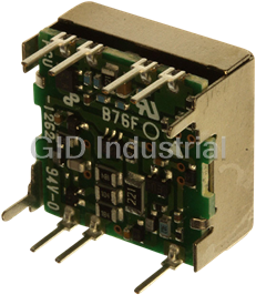
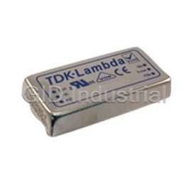
TDK-LAMBDA CC1R5-2403SF-E
Description
Lambda CC1R5-2403SF-E DC to DC Converter - Insulated Type, Ultra Compact Size, 1.5 to 25W Output
Part Number
CC1R5-2403SF-E
Price
Request Quote
Manufacturer
TDK-LAMBDA
Lead Time
Request Quote
Category
DC-DC Converters
Specifications
Current - Output (Max)
400mA
Lead Free Status
Lead Free
Number of Outputs
1
Power (Watts) - Manufacture Series
1W
RoHS Status
RoHS Compliant
Voltage - Input (Max)
36V
Voltage - Input (Min)
18V
Voltage - Isolation
500V
Voltage - Output 1
3.3V
Features
- All series are equipped with a built-in remote control function (except for SIP).
- Both mountings of DIP type and SMD type are available.
- Compact size(almost half floor space of existing product).
- It is a product conforming to RoHS directive.
- Light weight(no potting).
- No tantalum capacitor and no aluminum electrolytic capacitor are used.
- Output voltage tolerance ±3%(under 10W, at single output).
- These are PWB halogen-free pc board.
- UL60950-1, C-UL CSA 60950-1 and EN60950-1 approved(partial approved).
Datasheet

Extracted Text
(1/21) Conformity to RoHS Directive DC to DC Converters Insulated Type, Ultra Compact Size, 1.5 to 25W Output, 5-year Warranty Period CC-E Series FEATURES Compact size(almost half floor space of existing product). No tantalum capacitor and no aluminum electrolytic capacitor are used. All series are equipped with a built-in remote control function (except for SIP). Output voltage tolerance ±3%(under 10W, at single output). Light weight(no potting). It is a product conforming to RoHS directive. These are PWB halogen-free pc board. Both mountings of DIP type and SMD type are available. UL60950-1, C-UL CSA 60950-1 and EN60950-1 approved (partial approved). PART NUMBERS AND RATINGS Output voltage Output Input ∗2 ∗2 ∗3 power voltage 3.3V 5V 12V(15V)±12V(15V ) or 24V, 30V ∗1 5V CC1R5-0503Sx -E CC1R5-0505Sx-E CC1R5-0512Sx-E CC1R5-0512Dx-E 12V CC1R5-1203Sx-E CC1R5-1205Sx-E CC1R5-1212Sx-E CC1R5-1212Dx-E 1.5W 24V CC1R5-2403Sx-E CC1R5-2405Sx-E CC1R5-2412Sx-E CC1R5-2412Dx-E 48V CC1R5-4803Sx-E CC1R5-4805Sx-E CC1R5-4812Sx-E CC1R5-4812Dx-E 5V CC3-0503Sx-E CC3-0505Sx-E CC3-0512Sx-E CC3-0512Dx-E 12V CC3-1203Sx-E CC3-1205Sx-E CC3-1212Sx-E CC3-1212Dx-E 3W 24V CC3-2403Sx-E CC3-2405Sx-E CC3-2412Sx-E CC3-2412Dx-E 48V CC3-4803Sx-E CC3-4805Sx-E CC3-4812Sx-E CC3-4812Dx-E 5V CC6-0503Sx-E CC6-0505Sx-E CC6-0512Sx-E CC6-0512Dx-E 12V CC6-1203Sx-E CC6-1205Sx-E CC6-1212Sx-E CC6-1212Dx-E 6W 24V CC6-2403Sx-E CC6-2405Sx-E CC6-2412Sx-E CC6-2412Dx-E 48V CC6-4803Sx-E CC6-4805Sx-E CC6-4812Sx-E CC6-4812Dx-E 5V CC10-0503Sx-E CC10-0505Sx-E CC10-0512Sx-E CC10-0512Dx-E 12V CC10-1203Sx-E CC10-1205Sx-E CC10-1212Sx-E CC10-1212Dx-E 10W 24V CC10-2403Sx-E CC10-2405Sx-E CC10-2412Sx-E CC10-2412Dx-E 48V CC10-4803Sx-E CC10-4805Sx-E CC10-4812Sx-E CC10-4812Dx-E 15W 24V CC15-2403Sx-E CC15-2405Sx-E 25W 24V CC25-2403Sx-E CC25-2405Sx-E ∗1 An "x" within the product name is to be replaced by the symbol representing the terminal structure (F: DIP / R: SMD / S: SIP). Note that the SIP type is limited to 3W. ∗2 The output voltage can be set to 15V, ±15V, by connecting the 12Vout, ±12V TRM (output variable) to –Vout. ∗3 24V single output is possible by opening the ±12Vout COM terminal and connecting the load to +Vout, –Vout. Also, 30V single output is possible when connecting the TRM terminal with –Vout under the same conditions. PRODUCT IDENTIFICATIONS CC3-0505SF-E Form symbols F: Horizontal DIP type R: Horizontal SMD type S: Vertical SIP type Output mode symbols S: Single output, D: Double output Output voltage 03: 3.3V / 05: 5V / 12: 12V Input voltage 05: 5V / 12: 12V / 24: 24V / 48: 48V Output power 1R5: 1.5W / 3: 3W / 6:6W / 10: 10W / 15: 15W / 25: 25W Conformity to RoHS Directive: This means that, in conformity with EU Directive 2002/95/EC, lead, cadmium, mercury, hexavalent chromium, and specific bromine-based flame retardants, PBB and PBDE, have not been used, except for exempted applications. • All specifications are subject to change without notice. 002-05 / 20061129 / ea335_cc_e.fm (2/21) CC1R5 Type ELECTRICAL CHARACTERISTICS Voltage stability Output ripple noise Input Output Output Input- ∗5 ∗4 Efficiency voltage ∗2 ∗3 Part No. voltage current output voltage Input Load Temperature (mVp-p) (%) (V) (V) (mA) (mV)max. (mV)max. (mV)max. insulation typ./max. ∗1 CC1R5-0503Sx -E 4.5 to 9 3.3±3% 0 to 400 20 40 80 40/120 71 CC1R5-0505Sx-E 4.5 to 9 5±3% 0 to 300 20 40 80 40/120 77 4.5 to 9 12±3% 0 to 125 40 100 200 30/120 80 CC1R5-0512Sx-E ∗7 4.5 to 9 15±3% 0 to 100 40 100 200 30/120 80 4.5 to 9 ±12±5% ±0 to 60 80 600 300 30/120 79 ∗6 CC1R5-0512Dx-E ∗7 4.5 to 9 ±15±5% ±0 to 50 80 600 300 30/120 79 CC1R5-1203Sx-E 9 to 18 3.3±3% 0 to 400 20 40 80 40/120 73 CC1R5-1205Sx-E 9 to 18 5±3% 0 to 300 20 40 80 40/120 78 9 to 18 12±3% 0 to 125 40 100 200 30/120 82 Withstand CC1R5-1212Sx-E ∗7 9 to 18 15±3% 0 to 100 40 100 200 30/120 82 voltage 9 to 18 ±12±5% ±0 to 60 80 600 300 30/120 81 AC.500V ∗6 CC1R5-1212Dx-E ∗7 9 to 18 ±15±5% ±0 to 50 80 600 300 30/120 81 1min CC1R5-2403Sx-E 18 to 36 3.3±3% 0 to 400 20 40 80 40/120 72 Resistance DC.500V CC1R5-2405Sx-E 18 to 36 5±3% 0 to 300 20 40 80 40/120 77 50MΩ 18 to 36 12±3% 0 to 125 40 100 200 30/120 81 CC1R5-2412Sx-E min. ∗7 18 to 36 15±3% 0 to 100 40 100 200 30/120 81 18 to 36 ±12±5% ±0 to 60 80 600 300 30/120 79 ∗6 CC1R5-2412Dx-E ∗7 18 to 36 ±15±5% ±0 to 50 80 600 300 30/120 79 CC1R5-4803Sx-E 36 to 76 3.3±3% 0 to 400 20 40 80 40/120 70 CC1R5-4805Sx-E 36 to 76 5±3% 0 to 300 20 40 80 40/120 76 36 to 76 12±3% 0 to 125 40 100 200 30/120 80 CC1R5-4812Sx-E ∗7 36 to 76 15±3% 0 to 100 40 100 200 30/120 80 36 to 76 ±12±5% ±0 to 60 80 600 300 30/120 79 ∗6 CC1R5-4812Dx-E ∗7 36 to 76 ±15±5% ±0 to 50 80 600 300 30/120 79 ∗1 An "x" within the product name is to be replaced by the symbol representing the terminal structure (F: DIP / R: SMD). ∗2 Total output voltage is including input, load, and temperature regulation. ∗3 When the condition is 2-output, it is the balance load (balance load means the condition when the load current of +output and –output is equal). ∗4 Measurement bandwidth: 50MHz ∗5 Typical input voltage, maximum output current. ∗6 2-output products may be used as 24 to 30V single output with COM. terminal open. ∗7 TRM and –Vout are shorted. Trim range: 3.3Vout is 3.15 to 3.6V, 5Vout is 4.75 to 6V, 12Vout is 11.4 to 15V, ±12Vout is ±11.4 to ±15V (22.8 to 30V). OUTPUT POWER - AMBIENT TEMPERATURE(DERATING) COMMON SPECIFICATIONS Output current limitation system, auto recovery Overcurrent protection type 100 b Operating temperature –40 to +85°C[Derating is necessary when a 80 range operating environment temperature exceed 50°C] Natural cooling Storage temperature 60 –40 to +85°C range 40 95(%)RH max. Humidity range [Maximum wet-bulb temperature: 38°C] ( ) 20 a: 0.5m/s 100LFM 10 to 55Hz, all amplitude 1.52mm, sweep time ( ) b: 1m/s 200LFM Vibration 0 15min[3 directions of X, Y, Z, each 2h] –40–30–20–10 0 102030405060708090 2 Amplitude 980m/s (100G) 6ms[6 directions, each 3 times] Ambient temperature(˚C) Input to output, input to case, output to case: Withstand voltage Eac 500V, 1min Input to output, input to case, output to case: Insulation resistance 50MΩ min.[DC.500V] UL60950-1, C-UL(CSA22.2 No.60950-1), Safety standards EN60950-1 certified Weight 3.2g All specifications are subject to change without notice. 002-05 / 20061129 / ea335_cc_e.fm (%) Output power (3/21) CC1R5 Type SHAPES AND DIMENSIONS CC1R5-xxxxxF-E (DIP TYPE) RECOMMENDED PWB HOLE SIZE, LOCATION [TOP VIEW] 16.6±0.2 14.605 Shape 7-ø1.0 t=0.3 ( ) Land diameter ø2.0 12.7 16.51 2.7 a 1.905 12.7 1.905 2-ø1.5 (Land diameter ø2.5) 16.51 ab 1.0 3 4 b 2 5 2.7 7-0.3×0.6 6 Dimensions in mm 1 7 Tolerance: ±0.5 ba CC1R5-xxxxxR-E (SMD TYPE) RECOMMENDED PWB HOLE SIZE, LOCATION [TOP VIEW] 16.6±0.2 Shape t=0.3 16.51 Coplanarity 0.1max. 19.81 1.8 1.8 3.2 15.6 3.2 22.0 3 4 2 5 7-0.3×0.6 6 1 7 Dimensions in mm Tolerance: ±0.5 CONNECTIONS CC1R5-xxxxSx-E CC1R5-xxxxDx-E TERMINAL PIN TERMINAL PIN +Vin +Vout +Vin +Vout 1 7 1 7 CONFIGUTATION CONFIGUTATION 6 TRM 6 TRM No.1 +Vin No.1 +Vin 5 5 RC RC –Vout No.2 RC COM No.2 RC 2 2 No.3 –Vin No.3 –Vin –Vout 4NC 4 3 3 No.4 NC No.4 –Vout –Vin –Vin No.5 –Vout No.5 Common out No.6 TRM No.6 TRM No.7 +Vout No.7 +Vout All specifications are subject to change without notice. 002-05 / 20061129 / ea335_cc_e.fm 2.54 2.54 ( ) ( ) (3.22) 7.62 (3.22) 3.5 8.5max. 3.22 7.62 3.22 8.8max. 2.54 5.08 2.54 2.54 5.08 2.54 Load 0.5 3.5 0.5 4.0 4.0 13.08 (13.38) 10.16 10.16 7.62 2.92 ( ) 7.62 3.22 1.2 Load Load 2.54 5.08 2.54 2.54 5.08 2.54 (4/21) CC3 Type(DIP, SMD Types) ELECTRICAL CHARACTERISTICS Voltage stability Output ripple noise Input Output Output Input- ∗4 ∗5 voltage Efficiency ∗2 ∗3 Part No. voltage voltage current output Input Load Temperature (mVp-p) (%) (V) (V) (mA) (mV)max. (mV)max. (mV)max. insulation typ./max. ∗1 CC3-0503Sx -E 4.5 to 9 3.3±3% 0 to 800 20 40 80 40/120 73 CC3-0505Sx-E 4.5 to 9 5±3% 0 to 600 20 40 80 40/120 77 4.5 to 9 12±3% 0 to 250 40 100 200 30/120 82 CC3-0512Sx-E ∗7 4.5 to 9 15±3% 0 to 200 40 100 200 30/120 82 4.5 to 9 ±12±5% ±0 to 125 80 600 300 30/120 81 ∗6 CC3-0512Dx-E ∗7 4.5 to 9 ±15±5% ±0 to 100 80 600 300 30/120 81 CC3-1203Sx-E 9 to 18 3.3±3% 0 to 800 20 40 80 40/120 74 CC3-1205Sx-E 9 to 18 5±3% 0 to 600 20 40 80 40/120 79 9 to 18 12±3% 0 to 250 40 100 200 30/120 82 Withstand CC3-1212Sx-E ∗7 9 to 18 15±3% 0 to 200 40 100 200 30/120 82 voltage 9 to 18 ±12±5% ±0 to 125 80 600 300 30/120 81 AC.500V ∗6 CC3-1212Dx-E ∗7 9 to 18 ±15±5% ±0 to 100 80 600 300 30/120 81 1min CC3-2403Sx-E 18 to 36 3.3±3% 0 to 800 20 40 80 40/120 73 Resistance DC.500V CC3-2405Sx-E 18 to 36 5±3% 0 to 600 20 40 80 40/120 78 50MΩ 18 to 36 12±3% 0 to 250 40 100 200 30/120 82 CC3-2412Sx-E min. ∗7 18 to 36 15±3% 0 to 200 40 100 200 30/120 82 18 to 36 ±12±5% ±0 to 125 80 600 300 30/120 81 ∗6 CC3-2412Dx-E ∗7 18 to 36 ±15±5% ±0 to 100 80 600 300 30/120 81 CC3-4803Sx-E 36 to 76 3.3±3% 0 to 800 20 40 80 40/120 73 CC3-4805Sx-E 36 to 76 5±3% 0 to 600 20 40 80 40/120 79 36 to 76 12±3% 0 to 250 40 100 200 30/120 81 CC3-4812Sx-E ∗7 36 to 76 15±3% 0 to 200 40 100 200 30/120 81 36 to 76 ±12±5% ±0 to 125 80 600 300 30/120 80 ∗6 CC3-4812Dx-E ∗7 36 to 76 ±15±5% ±0 to 100 80 600 300 30/120 80 ∗1 An "x" within the product name is to be replaced by the symbol representing the terminal structure (F: DIP / R: SMD). ∗2 Total output voltage is including input, load, and temperature regulation. ∗3 When the condition is 2-output, it is the balance load (balance load means the condition when the load current of +output and –output is equal). ∗4 Measurement bandwidth: 50MHz ∗5 Typical input voltage, maximum output current. ∗6 2-output products may be used as 24 to 30V single output with COM. terminal open. ∗7 TRM and –Vout are shorted. Trim range: 3.3Vout is 3.15 to 3.6V, 5Vout is 4.75 to 6V, 12Vout is 11.4 to 15V, ±12Vout is ±11.4 to ±15V. OUTPUT POWER - AMBIENT TEMPERATURE(DERATING) COMMON SPECIFICATIONS Output current limitation system, auto recovery Overcurrent protection type 100 b Operating temperature –40 to +85°C[Derating is necessary when a 80 range operating environment temperature exceed 50°C] Natural cooling Storage temperature 60 –40 to +85°C range 40 95(%)RH max. Humidity range [Maximum wet-bulb temperature: 38°C] ( ) 20 a: 0.5m/s 100LFM 10 to 55Hz, all amplitude 1.52mm, sweep time ( ) b: 1m/s 200LFM Amplitude 0 15min[3 directions of X, Y, Z, each 2h] –40–30–20–10 0 102030405060708090 2 Vibration 980m/s (100G) 6ms[6 directions, each 3 times] Ambient temperature(˚C) Input to output, input to case, output to case: Withstand voltage Eac 500V, 1min Input to output, input to case, output to case: Insulation resistance 50MΩ min.[DC.500V] UL60950-1, C-UL(CSA22.2 No.60950-1), Safety standards EN60950-1 certified Weight 4.5g All specifications are subject to change without notice. 002-05 / 20061129 / ea335_cc_e.fm (%) Output power (5/21) CC3 Type(SIP Type) ELECTRICAL CHARACTERISTICS Voltage stability Output ripple noise Input Output Output Input- ∗3 ∗4 voltage Efficiency ∗1 ∗2 Part No. voltage voltage current output Input Load Temperature (mVp-p) (%) (V) (V) (mA) (mV)max. (mV)max. (mV)max. insulation typ./max. CC3-0503SS-E 4.5 to 9 3.3±3% 0 to 800 20 40 80 40/120 73 CC3-0505SS-E 4.5 to 9 5±3% 0 to 600 20 40 80 40/120 77 4.5 to 9 12±3% 0 to 250 40 100 200 30/120 82 CC3-0512SS-E ∗6 4.5 to 9 15±3% 0 to 200 40 100 200 30/120 82 4.5 to 9 ±12±5% ±0 to 125 80 600 300 30/120 81 ∗5 CC3-0512DS-E ∗6 4.5 to 9 ±15±5% ±0 to 100 80 600 300 30/120 81 CC3-1203SS-E 9 to 18 3.3±3% 0 to 800 20 40 80 40/120 73 CC3-1205SS-E 9 to 18 5±3% 0 to 600 20 40 80 40/120 79 9 to 18 12±3% 0 to 250 40 100 200 30/120 82 Withstand CC3-1212SS-E ∗6 9 to 18 15±3% 0 to 200 40 100 200 30/120 82 voltage 9 to 18 ±12±5% ±0 to 125 80 600 300 30/120 82 AC.500V ∗5 CC3-1212DS-E ∗6 9 to 18 ±15±5% ±0 to 100 80 600 300 30/120 82 1min CC3-2403SS-E 18 to 36 3.3±3% 0 to 800 20 40 80 40/120 73 Resistance DC.500V CC3-2405SS-E 18 to 36 5±3% 0 to 600 20 40 80 40/120 78 50MΩ 18 to 36 12±3% 0 to 250 40 100 200 30/120 82 CC3-2412SS-E min. ∗6 18 to 36 15±3% 0 to 200 40 100 200 30/120 82 18 to 36 ±12±5% ±0 to 125 80 600 300 30/120 81 ∗5 CC3-2412DS-E ∗6 18 to 36 ±15±5% ±0 to 100 80 600 300 30/120 81 CC3-4803SS-E 36 to 76 3.3±3% 0 to 800 20 40 80 40/120 73 CC3-4805SS-E 36 to 76 5±3% 0 to 600 20 40 80 40/120 79 36 to 76 12±3% 0 to 250 40 100 200 30/120 82 CC3-4812SS-E ∗6 36 to 76 15±3% 0 to 200 40 100 200 30/120 82 36 to 76 ±12±5% ±0 to 125 80 600 300 30/120 82 ∗5 CC3-4812DS-E ∗6 36 to 76 ±15±5% ±0 to 100 80 600 300 30/120 82 ∗1 Total output voltage is including input, load, and temperature regulation. ∗2 When the condition is 2-output, it is the balance load (balance load means the condition when the load current of +output and –output is equal). ∗3 Measurement bandwidth: 50MHz ∗4 Typical input voltage, maximum output current. ∗5 2-output products may be used as 24 to 30V single output with COM. terminal open. ∗6 TRM and –Vout are shorted. Trim range: 3.3Vout is 3.15 to 3.67V, 5Vout is 4.75 to 6V, 12Vout is 11.4 to 15V, ±12Vout is ±11.4 to ±15V. OUTPUT POWER - AMBIENT TEMPERATURE(DERATING) COMMON SPECIFICATIONS Output current limitation system, auto recovery Overcurrent protection type 100 b Operating temperature –40 to +85°C[Derating is necessary when a 80 range operating environment temperature exceed 50°C] Natural cooling Storage temperature 60 –40 to +85°C range 40 95(%)RH max. Humidity range [Maximum wet-bulb temperature: 38°C] ( ) 20 a: 0.5m/s 100LFM ( ) 10 to 55Hz, all amplitude 1.52mm, sweep time b: 1m/s 200LFM Amplitude 0 15min[3 directions of X, Y, Z, each 2h] –40–30–20–10 0 102030405060708090 2 Vibration 980m/s (100G) 6ms[6 directions, each 3 times] (˚C) Ambient temperature Input to output, input to case, output to case: Withstand voltage Eac 500V, 1min Input to output, input to case, output to case: Insulation resistance 50MΩ min.[DC.500V] UL60950-1, C-UL(CSA22.2 No.60950-1), Safety standards EN60950-1 certified is applying partially. Weight 7.0g All specifications are subject to change without notice. 002-05 / 20061129 / ea335_cc_e.fm (%) Output power (6/21) CC3 Type(DIP, SMD Types) SHAPES AND DIMENSIONS CC3-xxxxxF-E (DIP TYPE) RECOMMENDED PWB HOLE SIZE, LOCATION [TOP VIEW] 16.6±0.2 20.32 Shape t=0.3 ( ) 7-ø1.0 Land diameter ø2.0 17.78 22.86 2.7 2.54 17.78 2.54 2-ø1.5(Land diameter ø2.5) a 22.86 a b 3 4 1.0 2 5 b 7-0.3×0.6 2.7 6 1 7 Dimensions in mm ba Tolerance: ±0.5 CC3-xxxxxR-E (SMD TYPE) RECOMMENDED PWB HOLE SIZE, LOCATION [TOP VIEW] 16.6±0.2 Shape t=0.3 22.86 Coplanarity 0.1max. 26.16 3.2 22.0 3.2 1.8 1.8 28.4 3 4 2 5 7-0.3×0.6 6 1 7 Dimensions in mm Tolerance: ±0.5 CONNECTIONS CC3-xxxxSx-E CC3-xxxxDx-E TERMINAL PIN TERMINAL PIN +Vin +Vout +Vin +Vout 1 7 1 7 CONFIGUTATION CONFIGUTATION 6 TRM 6 TRM No.1 +Vin No.1 +Vin 5 5 RC RC COM No.2 RC –Vout No.2 RC 2 2 No.3 –Vin No.3 –Vin –Vout 4NC 3 4 3 No.4 NC No.4 –Vout –Vin –Vin No.5 –Vout No.5 Common out No.6 TRM No.6 TRM No.7 +Vout No.7 +Vout All specifications are subject to change without notice. 002-05 / 20061129 / ea335_cc_e.fm 2.54 2.54 (3.22) 7.62 (3.22) ( ) ( ) 3.22 7.62 3.22 3.5 8.5max. 8.8max. Load 2.54 5.08 2.54 2.54 5.08 2.54 0.5 3.5 0.5 4.0 4.0 ( ) 13.08 13.38 10.16 10.16 ( ) 7.62 2.92 7.62 3.22 1.2 Load Load 2.54 5.08 2.54 2.54 5.08 2.54 (7/21) CC3 Type(SIP Type) SHAPES AND DIMENSIONS CC3-xxxxxS-E (SIP TYPE) 9.2 ( ) 1 t=0.3 2.47 P P P P 2P P P P P 2.47 6 22.86 17.78 5.01 P=2.54 27.8 a RECOMMENDED PWB HOLE SIZE, LOCATION a 12345 789 10 [TOP VIEW] 4 27.8 2.47 22.86 2.47 17.78 ( ) 2-ø1.5 Land diameter ø2.5 SMD location P=2.54 Dimensions in mm PPPP 2P PPP Tolerance: ±0.5 9-ø0.8(Land diameter ø2.0) CONNECTIONS CC3-xxxxSS-E CC3-xxxxDS-E TERMINAL PIN TERMINAL PIN CONFIGUTATION CONFIGUTATION No.1 +Vout No.1 +Vout 1234 5 7 8 9 10 1234 5 7 8 9 10 No.2 NC No.2 COM No.3 NC No.3 COM Load No.4 –Vout No.4 –Vout Load Load No.5 TRM No.5 TRM No.6 NC No.6 NC No.7 –Vin No.7 –Vin No.8 –Vin No.8 –Vin No.9 +Vin No.9 +Vin No.10 +Vin No.10 +Vin The output voltage can be set to 15V, ±15V, by connecting the output variable terminal TRM of the 12Vout, ±12V output model to –Vout. 24V single output is possible by opening the ±12Vout COM terminal and connecting the load to +Vout, –Vout. Also, 30V single output is possible when connecting the TRM terminal with –Vout under the same conditions. All specifications are subject to change without notice. 002-05 / 20061129 / ea335_cc_e.fm +Vout –Vout TRM –Vin –Vin +Vin +Vin 9.2 4.1 17.9 ( ) 0.5 0.5 3.5 (0.5) +Vout COM COM –Vout TRM –Vin –Vin +Vin +Vin 6.0 9.2 (8/21) CC6 Type ELECTRICAL CHARACTERISTICS Voltage stability Output ripple noise Input Output Output Input- ∗4 ∗5 voltage Efficiency ∗2 ∗3 Part No. voltage voltage current output Input Load Temperature (mVp-p) (%) (V) (V) (mA) (mV)max. (mV)max. (mV)max. insulation typ./max. ∗1 CC6-0503Sx -E 4.5 to 9 3.3±3% 0 to 1200 20 40 80 40/120 76 CC6-0505Sx-E 4.5 to 9 5±3% 0 to 1000 20 40 80 40/120 79 4.5 to 9 12±3% 0 to 500 40 100 200 30/120 82 CC6-0512Sx-E ∗7 4.5 to 9 15±3% 0 to 400 40 100 200 30/120 82 4.5 to 9 ±12±5% ±0 to 250 80 600 300 30/120 82 ∗6 CC6-0512Dx-E ∗7 4.5 to 9 ±15±5% ±0 to 200 80 600 300 30/120 82 CC6-1203Sx-E 9 to 18 3.3±3% 0 to 1200 20 40 80 40/120 78 CC6-1205Sx-E 9 to 18 5±3% 0 to 1200 20 40 80 40/120 82 9 to 18 12±3% 0 to 500 40 100 200 30/120 85 Withstand CC6-1212Sx-E ∗7 9 to 18 15±3% 0 to 400 40 100 200 30/120 85 voltage 9 to 18 ±12±5% ±0 to 250 80 600 300 30/120 85 AC.500V ∗6 CC6-1212Dx-E ∗7 9 to 18 ±15±5% ±0 to 200 80 600 300 30/120 85 1min CC6-2403Sx-E 18 to 36 3.3±3% 0 to 1200 20 40 80 40/120 77 Resistance DC.500V CC6-2405Sx-E 18 to 36 5±3% 0 to 1200 20 40 80 40/120 81 50MΩ 18 to 36 12±3% 0 to 500 40 100 200 30/120 87 CC6-2412Sx-E min. ∗7 18 to 36 15±3% 0 to 400 40 100 200 30/120 87 18 to 36 ±12±5% ±0 to 250 80 600 300 30/120 86 ∗6 CC6-2412Dx-E ∗7 18 to 36 ±15±5% ±0 to 200 80 600 300 30/120 86 CC6-4803Sx-E 36 to 76 3.3±3% 0 to 1200 20 40 80 40/120 77 CC6-4805Sx-E 36 to 76 5±3% 0 to 1200 20 40 80 40/120 81 36 to 76 12±3% 0 to 500 40 100 200 30/120 86 CC6-4812Sx-E ∗7 36 to 76 15±3% 0 to 400 40 100 200 30/120 86 36 to 76 ±12±5% ±0 to 250 80 600 300 30/120 86 ∗6 CC6-4812Dx-E ∗7 36 to 76 ±15±5% ±0 to 200 80 600 300 30/120 86 ∗1 An "x" within the product name is to be replaced by the symbol representing the terminal structure (F: DIP / R: SMD). ∗2 Total output voltage is including input, load, and temperature regulation. ∗3 When the condition is 2-output, it is the balance load (balance load means the condition when the load current of +output and –output is equal). ∗4 Measurement bandwidth: 50MHz ∗5 Typical input voltage, maximum output current ∗6 2-output products may be used as 24 to 30V single output with COM. terminal open. ∗7 TRM and –Vout are shorted. Trim range: 3.3Vout is 3.15 to 3.6V, 5Vout is 4.75 to 6V, 12Vout is 11.4 to 15V, ±12Vout is ±11.4 to ±15V. OUTPUT POWER - AMBIENT TEMPERATURE(DERATING) COMMON SPECIFICATIONS Output current limitation system, auto recovery Overcurrent protection type 100 b Operating temperature –40 to +85°C[Derating is necessary when a 80 range operating environment temperature exceed 50°C] Natural cooling Storage temperature 60 –40 to +85°C range 40 95(%)RH max. Humidity range [Maximum wet-bulb temperature: 38°C] ( ) 20 a: 0.5m/s 100LFM 10 to 55Hz, all amplitude 1.52mm, sweep time ( ) b: 1m/s 200LFM Amplitude 0 15min[3 directions of X, Y, Z, each 2h] –40–30–20–10 0 102030405060708090 2 Vibration 980m/s (100G) 6ms[6 directions, each 3 times] Ambient temperature(˚C) Input to output, input to case, output to case: Withstand voltage Eac 500V, 1min Input to output, input to case, output to case: Insulation resistance 50MΩ min.[DC.500V] UL60950-1, C-UL(CSA22.2 No.60950-1), Safety standards EN60950-1 certified Weight 5.8g All specifications are subject to change without notice. 002-05 / 20061129 / ea335_cc_e.fm (%) Output power (9/21) CC6 Type SHAPES AND DIMENSIONS CC6-xxxxxF-E (DIP TYPE) RECOMMENDED PWB HOLE SIZE, LOCATION [TOP VIEW] 21.1±0.2 20.32 Shape t=0.3 ( ) 7-ø1.0 Land diameter ø2.0 17.78 22.86 b 2.7 2.54 2.54 ( ) 2-ø1.5 Land diameter ø2.5 a b 22.86 1.0 3 4 7-0.3×0.6 a 2 5 2.7 6 Dimensions in mm 1 7 Tolerance: ±0.5 ba CC6-xxxxxR-E (SMD TYPE) RECOMMENDED PWB HOLE SIZE, LOCATION [TOP VIEW] 21.1±0.2 Shape t=0.3 22.86 Coplanarity 0.1max. 26.16 1.8 1.8 3 4 3.2 22.0 3.2 7-0.3×0.6 28.4 2 5 6 1 7 Dimensions in mm Tolerance: ±0.5 CONNECTIONS CC6-xxxxSx-E CC6-xxxxDx-E TERMINAL PIN TERMINAL PIN +Vin +Vout +Vin +Vout 1 7 1 7 CONFIGUTATION CONFIGUTATION 6 TRM 6 TRM No.1 +Vin No.1 +Vin 5 5 RC RC –Vout COM No.2 RC No.2 RC 2 2 No.3 –Vin No.3 –Vin –Vout 4NC 4 3 3 No.4 NC No.4 –Vout –Vin –Vin No.5 –Vout No.5 Common out No.6 TRM No.6 TRM No.7 +Vout No.7 +Vout All specifications are subject to change without notice. 002-05 / 20061129 / ea335_cc_e.fm (2.93) 10.16 5.08 (2.93) 8.8max. (2.93) 10.16 5.08 (2.93) 3.5 8.5max. 5.08 5.08 5.08 Load 5.08 5.08 5.08 0.5 3.5 0.5 4.0 4.0 ( ) 18.17 17.87 15.24 15.24 10.16 (2.93) 10.16 2.63 1.2 Load Load 5.08 5.08 5.08 5.08 5.08 5.08 (10/21) CC10 Type ELECTRICAL CHARACTERISTICS Voltage stability Output ripple noise Input Output Output Input- ∗4 ∗5 voltage Efficiency ∗2 ∗3 Part No. voltage voltage current output Input Load Temperature (mVp-p) (%) (V) (V) (mA) (mV)max. (mV)max. (mV)max. insulation typ./max. ∗1 CC10-0503Sx -E 4.5 to 9 3.3±3% 0 to 2500 20 40 80 40/120 84 CC10-0505Sx-E 4.5 to 9 5±3% 0 to 2000 20 40 80 40/120 84 4.5 to 9 12±3% 0 to 800 40 100 200 30/120 84 CC10-0512Sx-E ∗7 4.5 to 9 15±3% 0 to 640 40 100 200 30/120 84 4.5 to 9 ±12±5% ±0 to 400 80 600 300 30/120 83 ∗6 CC10-0512Dx-E ∗7 4.5 to 9 ±15±5% ±0 to 320 80 600 300 30/120 83 CC10-1203Sx-E 9 to 18 3.3±3% 0 to 2500 20 40 80 40/120 84 CC10-1205Sx-E 9 to 18 5±3% 0 to 2000 20 40 80 40/120 86 9 to 18 12±3% 0 to 1000 40 100 200 30/120 88 Withstand CC10-1212Sx-E ∗7 9 to 18 15±3% 0 to 800 40 100 200 30/120 88 voltage 9 to 18 ±12±5% ±0 to 450 80 600 300 30/120 86 AC.500V ∗6 CC10-1212Dx-E ∗7 9 to 18 ±15±5% ±0 to 360 80 600 300 30/120 86 1min CC10-2403Sx-E 18 to 36 3.3±3% 0 to 2500 20 40 80 40/120 84 Resistance DC.500V CC10-2405Sx-E 18 to 36 5±3% 0 to 2000 20 40 80 40/120 86 50MΩ 18 to 36 12±3% 0 to 1000 40 100 200 30/120 87 CC10-2412Sx-E min. ∗7 18 to 36 15±3% 0 to 800 40 100 200 30/120 87 18 to 36 ±12±5% ±0 to 450 80 600 300 30/120 86 ∗6 CC10-2412Dx-E ∗7 18 to 36 ±15±5% ±0 to 360 80 600 300 30/120 86 CC10-4803Sx-E 36 to 76 3.3±3% 0 to 2500 20 40 80 40/120 84 CC10-4805Sx-E 36 to 76 5±3% 0 to 2000 20 40 80 40/120 86 36 to 76 12±3% 0 to 1000 40 100 200 30/120 88 CC10-4812Sx-E ∗7 36 to 76 15±3% 0 to 800 40 100 200 30/120 88 36 to 76 ±12±5% ±0 to 450 80 600 300 30/120 86 ∗6 CC10-4812Dx-E ∗7 36 to 76 ±15±5% ±0 to 360 80 600 300 30/120 86 ∗1 An "x" within the product name is to be replaced by the symbol representing the terminal structure (F: DIP / R: SMD). ∗2 Total output voltage is including input, load, and temperature regulation. ∗3 When the condition is 2-output, it is the balance load (balance load means the condition when the load current of +output and –output is equal). ∗4 Measurement bandwidth: 50MHz ∗5 Typical input voltage, maximum output current ∗6 2-output products may be used as 24 to 30V single output with COM. terminal open. ∗7 TRM and –Vout are shorted. Trim range: 3.3Vout is 3.15 to 3.6V, 5Vout is 4.75 to 6V, 12Vout is 11.4 to 15V, ±12Vout is ±11.4 to ±15V. OUTPUT POWER - AMBIENT TEMPERATURE(DERATING) COMMON SPECIFICATIONS Output current limitation system, auto recovery Overcurrent protection type 100 b Operating temperature –40 to +85°C[Derating is necessary when a 80 range operating environment temperature exceed 50°C] Natural cooling Storage temperature 60 –40 to +85°C range 40 95(%)RH max. Humidity range [Maximum wet-bulb temperature: 38°C] ( ) 20 a: 0.5m/s 100LFM 10 to 55Hz, all amplitude 1.52mm, sweep time ( ) b: 1m/s 200LFM Amplitude 0 15min[3 directions of X, Y, Z, each 2h] –40–30–20–10 0 102030405060708090 2 Vibration 980m/s (100G) 6ms[6 directions, each 3 times] Ambient temperature(˚C) Input to output, input to case, output to case: Withstand voltage Eac 500V, 1min Input to output, input to case, output to case: Insulation resistance 50MΩ min.[DC.500V] UL60950-1, C-UL(CSA22.2 No.60950-1), Safety standards EN60950-1 certified Weight 10.0g All specifications are subject to change without notice. 002-05 / 20061129 / ea335_cc_e.fm (%) Output power (11/21) CC10 Type SHAPES AND DIMENSIONS CC10-xxxxxF-E (DIP TYPE) RECOMMENDED PWB HOLE SIZE, LOCATION [TOP VIEW] 22.6±0.2 30.48 Shape t=0.3 ( ) 7-ø1.0 Land diameter ø2.0 25.4 35.56 a 5.08 25.4 5.08 2.7 ( ) 2-ø1.5 Land diameter ø2.5 b 35.56 a b 2.7 3 4 2 5 6 7-0.3×0.6 1.0 Dimensions in mm 1 7 Tolerance: ±0.5 b a CC10-xxxxxR-E (SMD TYPE) RECOMMENDED PWB HOLE SIZE, LOCATION [TOP VIEW] 22.6±0.2 Shape t=0.3 35.56 Coplanarity 0.1max. 38.86 1.8 1.8 3.2 34.6 3.2 3 4 41.0 2 5 6 7-0.3×0.6 1 7 Dimensions in mm Tolerance: ±0.5 CONNECTIONS CC10-xxxxSx-E CC10-xxxxDx-E TERMINAL PIN TERMINAL PIN +Vin +Vout +Vin +Vout 1 7 1 7 CONFIGUTATION CONFIGUTATION 6 TRM 6 TRM No.1 +Vin No.1 +Vin 5 5 RC No.2 RC RC No.2 RC –Vout COM 2 2 No.3 –Vin No.3 –Vin –Vout 4NC No.4 NC 4 3 3 No.4 –Vout –Vin –Vin No.5 –Vout No.5 Common out No.6 TRM No.6 TRM No.7 +Vout No.7 +Vout All specifications are subject to change without notice. 002-05 / 20061129 / ea335_cc_e.fm 5.08 5.08 (3.68) 10.16 (3.68) ( ) ( ) 3.68 10.16 3.68 3.5 8.5max. 8.8max. Load 5.08 5.08 5.08 5.08 5.08 5.08 4.0 3.5 0.5 0.5 4.0 ( ) 18.92 18.62 15.24 15.24 ( ) 10.16 3.68 10.16 3.38 1.2 Load Load 5.08 5.08 5.08 5.08 5.08 5.08 (12/21) CC15 Type ELECTRICAL CHARACTERISTICS Voltage stability Output ripple noise Input Output Output Input- ∗3 ∗4 voltage Efficiency ∗2 Part No. voltage voltage current output Input Load Temperature (mVp-p) (%) (V) (V) (mA) (mV)max. (mV)max. (mV)max. insulation typ./max. Withstand voltage ∗1 CC15-2403Sx -E 18 to 36 3.3/–3 to +5% 0 to 4500 40 120 80 40/120 89 AC.500V 1min Resistance DC.500V CC15-2405Sx-E 18 to 36 5.0/–3 to +5% 0 to 3000 50 200 80 40/120 89 50MΩ min. ∗1 An "x" within the product name is to be replaced by the symbol representing the terminal structure (F: DIP / R: SMD). ∗2 Total output voltage is including input, load, and temperature regulation. ∗3 Measurement bandwidth: 50MHz ∗4 Typical input voltage, maximum output current OUTPUT POWER - AMBIENT TEMPERATURE(DERATING) COMMON SPECIFICATIONS Output current limitation system, Output voltage Overcurrent protection shut-down type 100 b Operating temperature –40 to +85°C[Derating is necessary when a 80 range operating environment temperature exceed 50°C] Natural cooling Storage temperature 60 –40 to +85°C range 40 95(%)RH max. Humidity range [Maximum wet-bulb temperature: 38°C] ( ) 20 a: 0.5m/s 100LFM ( ) 10 to 55Hz, all amplitude 1.52mm, sweep time b: 1m/s 200LFM Amplitude 0 15min[3 directions of X, Y, Z, each 2h] –40–30–20–10 0 102030405060708090 2 Vibration 980m/s (100G) 6ms[6 directions, each 3 times] (˚C) Ambient temperature Input to output, input to case, output to case: Withstand voltage Eac 500V, 1min Input to output, input to case, output to case: Insulation resistance 50MΩ min[DC.500V] UL60950-1, C-UL(CSA22.2 No.60950-1), Safety standards EN60950-1 certified Weight 12.5g All specifications are subject to change without notice. 002-05 / 20061129 / ea335_cc_e.fm (%) Output power (13/21) CC15 Type SHAPES AND DIMENSIONS CC15-xxxxSF-E (DIP TYPE) RECOMMENDED PWB HOLE SIZE, LOCATION 38.1 32.1 [TOP VIEW] Shape t=0.3 6.075 25.4 6.075 37.55 2.7 a ( ) 17-ø1.0 Land diameter ø2.0 a b 10 11 9 12 8 13 1.0 7 14 ( ) 2-ø1.5 Land diameter ø2.5 6 15 5 16 b 4 3 6.075 17-0.3×0.6 2.7 2 31.475 1 17 ba P=2.54 37.55 Dimensions in mm Tolerance: ±0.5 CC15-xxxxSR-E (SMD TYPE) RECOMMENDED PWB HOLE SIZE, LOCATION [TOP VIEW] 38.1 32.1 Shape t=0.3 40.9 Coplanarity 0.1max. 22 21 10 11 9 12 8 13 7 14 6 15 5 16 4 3 17-0.3×0.6 2 1 3.2 36.6 3.2 17 20 18 43.0 P=2.54 1.8 1.8 Dimensions in mm Tolerance: ±0.5 CONNECTION TERMINAL PIN CONFIGUTATION 1 17 RC 2 No.1 NC No.10 NC 3 No.2 NC No.11 NC 4 –Vout 5 16 No.3 RC No.12 +Vout +Vin 6 15 No.4 NC No.13 +Vout 7 14 No.5 NC No.14 +Vout 8 13 9 12 No.6 +Vin No.15 –Vout +Vout –Vin 10 11 No.7 +Vin No.16 –Vout No.8 –Vin No.17 NC No.9 –Vin All specifications are subject to change without notice. 002-05 / 20061129 / ea335_cc_e.fm (4.62) 2.54 (4.62) 7.5max. ( ) ( ) 4.62 2.54 4.62 3.0 7.0max. 10.16 2.54 10.16 2.54 Load 0.5 3.5 0.5 27.33 27.33 22.86 22.86 4.47 P PPPPPPPP 4.47 PPPPPPPP 1.2 PPPPP 10.16 PPPPP 10.16 (14/21) CC25 Type ELECTRICAL CHARACTERISTICS Voltage stability Output ripple noise Input Output Output Input- ∗3 ∗4 voltage Efficiency ∗2 Part No. voltage voltage current output Input Load Temperature (mVp-p) (%) (V) (V) (mA) (mV)max. (mV)max. (mV)max. insulation typ./max. Withstand voltage ∗1 CC25-2403Sx -E 18 to 36 3.3/–3 to +5% 0 to 7500 40 120 80 40/120 90 AC.500V 1min Resistance DC.500V CC25-2405Sx-E 18 to 36 5.0/–3 to +5% 0 to 5000 50 200 80 40/120 90 50MΩ min. ∗1 An "x" within the product name is to be replaced by the symbol representing the terminal structure (F: DIP / R: SMD). ∗2 Total output voltage is including input, load, and temperature regulation. ∗3 Measurement bandwidth: 50MHz ∗4 Typical input voltage, maximum output current OUTPUT POWER - AMBIENT TEMPERATURE(DERATING) COMMON SPECIFICATIONS Output current limitation system, Output voltage Overcurrent protection shut-down type 100 b Operating temperature –40 to +85°C[Derating is necessary when a 80 range operating environment temperature exceed 50°C] Natural cooling Storage temperature 60 –40 to +85°C range 40 95(%)RH max. Humidity range [Maximum wet-bulb temperature: 38°C] ( ) 20 a: 0.5m/s 100LFM ( ) 10 to 55Hz, all amplitude 1.52mm, sweep time b: 1m/s 200LFM Amplitude 0 15min[3 directions of X, Y, Z, each 2h] –40–30–20–10 0 102030405060708090 2 Vibration 500m/s (51G) 6ms[6 directions, each 3 times] (˚C) Ambient temperature Input to output, input to case, output to case: Withstand voltage Eac 500V, 1min Input to output, input to case, output to case: Insulation resistance 50MΩ min.[DC.500V] UL60950-1, C-UL(CSA22.2 No.60950-1), Safety standards EN60950-1 certified Weight 20.0g All specifications are subject to change without notice. 002-05 / 20061129 / ea335_cc_e.fm (%) Output power (15/21) CC25 Type SHAPES AND DIMENSIONS CC25-xxxxSF-E (DIP TYPE) RECOMMENDED PWB HOLE SIZE, LOCATION 43.2 44.9 [TOP VIEW] t=0.3 Shape 6.075 30.5 6.075 42.65 2.7 b ( ) 25-ø1.0 Land diameter ø2.0 a b 13 14 12 15 11 16 10 17 1.0 18 9 19 2-ø1.5 a 8 20 ( ) 7 25-0.3×0.6 Land diameter ø2.5 21 22 2.7 6 23 6.075 5 24 4 36.575 3 2 42.65 P=2.54 25 1 ba Dimensions in mm Tolerance: ±0.5 CC25-xxxxSR-E (SMD TYPE) RECOMMENDED PWB HOLE SIZE, LOCATION 43.2 44.9 [TOP VIEW] t=0.3 Shape 46.0 Coplanarity 0.1max. 1.8 1.8 13 14 15 12 11 16 10 17 18 9 19 8 20 21 7 22 6 23 5 24 4 3.2 41.7 3.2 3 48.1 P=2.54 2 25 1 Dimensions in mm Tolerance: ±0.5 CONNECTION TERMINAL PIN CONFIGUTATION 1 25 –Vout No.1 NC No.10 +Vin No.19 –Vout 2 24 RC 3 23 No.2 NC No.11 +Vin No.20 –Vout 4 22 No.3 NC No.12 +Vin No.21 –Vout 5 21 6 No.4 RC No.13 NC No.22 –Vout –Vin 20 7 19 No.5 NC No.14 NC No.23 –Vout 8 18 No.6 NC No.15 +Vout No.24 –Vout 9 17 10 No.7 –Vin No.16 +Vout No.25 NC 16 11 No.8 –Vin No.17 +Vout 12 15 +Vin +Vout 13 14 No.9 –Vin No.18 +Vout All specifications are subject to change without notice. 002-05 / 20061129 / ea335_cc_e.fm 2.54 5.08 5.08 2.54 5.08 5.08 3.0 7.0max. 7.5max. (4.67) 10.16 (4.67) ( ) ( ) 4.67 10.16 4.67 Load 0.5 3.5 0.5 40.08 40.08 35.56 35.56 5.08 5.08 5.08 5.08 PP P P P PP P P P 4.52 PP P P P PP P P P 4.52 P P PPP P PPPP 10.16 P P PPP P PPPP 10.16 (16/21) Control Functions/Connections REMOTE CONTROL TERMINAL(RC) OUTPUT VARIABLE TERMINAL(TRM) (DIP/SMD MODELS) (1.5 to 10W Types) 1.5 to 10W Types The output voltage can be set to the value shown in the following It is recommended to use an open collector as the control method table by connecting the TRM terminal with the –Vout terminal. for the remote control terminal. If other methods are necessary, Please open the TRM terminal when not using this function. please contact TDK first. Please take note that it is necessary to derate the output current to In addition, please use a transistor with VCE: Over Vin and Ic: Over match the maximum power when the output voltage is set higher 1mA. by this function. When the RC terminal is open, the output is OFF, and when the RC terminal and –Vin are shorted (0 to 0.4V) the output is ON. DIP/SMD Models Part No. Open Connected with –Vout Fig. +Vin +Vout ∗ CCx –xx03Sx 3.3V 3.6V 1 RC CCx–xx05Sx 5.0V 6.0V 1 control RC signal CCx–xx12Sx 12V 15V 1 CCx–xx12Dx ±12V ±15V 2 ∗ –Vin –Vout To be replaced by 1R5(1.5W), 3(3W), 6(6W) and 10(10W). If not using this function (always ON), short-circuit the RC terminal Fig.1 and the –Vin terminal. 3.3V 3.6V 5V 6V +Vin +Vout +Vin +Vout 12V 15V +Vin +Vout TRM TRM When not used RC (Always ON) –Vin –Vout –Vin –Vout –Vin –Vout Fig.2 +12V +15V 15 and 25W Types +Vin +Vout +Vin +Vout When the RC terminal is open, the output is ON, and when the RC TRM Load TRM Load terminal is HIGH (connected to +Vin) the output is OFF. COM COM Load Load +Vin +Vout –Vin –Vout –Vin –Vout –12V –15V RC RC control SIP Model signal Part No. Open Connected with –Vout Fig. –Vin –Vout CC3–xx03SS–E 3.3V 3.67V 3 CC3–xx05SS–E 5V 6V 3 If not using this function (always ON), short-circuit the RC terminal CC3–xx12SS–E 12V 15V 3 and the –Vin terminal. CC3–xx12DS–E ±12V ±15V 4 +Vin +Vout Fig.3 When not used RC (Always ON) –Vin –Vout Load Load 3.3V, 5V, 12V 3.67V, 6V, 15V Fig.4 Load Load Load Load +12V –12V +15V –15V All specifications are subject to change without notice. 002-05 / 20061129 / ea335_cc_e.fm Load Load Load Load +Vout +Vout COM –Vout TRM –Vout TRM –Vin Load –Vin +Vin +Vin +Vout +Vout COM –Vout –Vout TRM TRM Load –Vin –Vin +Vin +Vin (17/21) Control Functions/Connections With the ±12V, 24V single output is possible by opening the COM OUTPUT VARIABILITY FUNCTION terminal and TRM terminal. Also, 30V single output is possible (ADDING EXTERNAL RESISTANCE) (1.5 to 10W Types) when opening the COM terminal and connecting the TRM terminal The output voltage can be adjusted within the range shown in the with the –Vout terminal. following table by connecting resistance (Ra, Rb) between the DIP/SMD Models TRM terminal and the –Vout terminal, or between the TRM termi- Part No. COM terminal TRM terminal Single output Fig. nal and the +Vout terminal. Open Open 24V 5 Please take note that it is necessary to derate the output current to ∗ CCx –xx12Dx–E Connected with match the maximum power when the output voltage is setted Open 30V 6 –Vout higher. ∗ To be replaced by 1R5(1.5W), 3(3W), 6(6W) and 10(10W). DIP/SMD Models Fig.5 Fig.6 Connecting –Vout Connecting +Vout Part No. Fig. Fig. +Vin +Vout +Vin +Vout with Ra with Rb 24V 30V ∗ ∗1 ∗5 TRM CCx –xx03Sx–E 3.3 to 3.6V 9 3.15 to 3.3V 10 TRM ∗2 ∗6 CCx–xx05Sx–E 5 to 6V 9 4.75 to 5V 10 COM COM ∗3 ∗7 CCx–xx12Sx–E 12 to 15V 9 11.4 to 12V 10 –Vin –Vout ∗4 ∗8 –Vin –Vout CCx–xx12Dx–E ±12 to ±15V 11 ±11.4 to ±12V 12 ∗ To be replaced by 1R5(1.5W), 3(3W), 6(6W) and 10(10W). SIP Model Calculate the output voltage Vout(V) from the connected resistance Ra, Rb(kΩ) Part No. COM terminal TRM terminal Single output Fig. Set the output voltage higher by adding resistance Ra between Open Open 24V 7 the TRM terminal/–Vout terminal. CC3–xx12DS–E Connected with Open 30V 8 ∗1 Vout=3.3+9.59/(32+Ra) –Vout ∗2 Vout=5.01+17.64/(17.8+Ra) ∗3 Vout=12.01+50.53/(16.9+Ra) Fig.7 Fig.8 ∗4 Vout=12.02+53.55/(18+Ra) Set the output voltage lower by adding resistance Rb between the TRM terminal/+Vout terminal. ∗5 Vout=3.3–15.53/(39.6+Rb) [Rb 62] Load Load ∗6 24V 30V Vout=5.01–52.55/(31.8+Rb) [Rb 160] ∗7 Vout=12.01–431.1/(57+Rb) [Rb 620] ∗8 Vout=12.02–968.5/(103+Rb) [Rb 1500] Calculate the connected resistance Ra and Rb(kΩ) from the set output voltage Vout(V). Set the output voltage higher by adding resistance Ra between the TRM terminal/–Vout terminal. ∗1 Ra=9.59/(Vout–3.3)–32 ∗2 Ra=17.64/(Vout–5.01)–17.8 ∗3 Ra=50.53/(Vout–12.01)–16.9 ∗4 Ra=53.55/(Vout–12.02)–18 Set the output voltage lower by adding resistance Rb between the TRM terminal/+Vout terminal. ∗5 Rb=15.53/(3.3–Vout)–39.6 ∗6 Rb=52.55/(5.01–Vout)–31.8 ∗7 Rb=431.1/(12.01–Vout)–57 ∗8 Rb=968.5/(12.02–Vout)–103 Fig.9 Fig.10 3.3 to 3.6V 3.15 to 3.3V +Vout 5 to 6V +Vout 4.75 to 5V 12 to 15V 11.4 to 12V Rb TRM TRM Ra –Vout –Vout Fig.11 Fig.12 +12 to +15V +11.4 to +12V +Vout +Vout Rb TRM Load TRM Load COM COM Load Load Ra –Vout –Vout –12 to –15V –11.4 to –12V All specifications are subject to change without notice. 002-05 / 20061129 / ea335_cc_e.fm +Vout COM –Vout TRM Load –Vin +Vin +Vout COM –Vout TRM –Vin Load +Vin Load Load (18/21) Control Functions/Connections SIP Model Connecting –Vout Connecting +Vout Part No. Fig. Fig. with Ra with Rb ∗1 ∗5 CC3–xx03SS–E 3.3 to 3.67V 13 3.15 to 3.3V 14 ∗2 ∗6 CC3–xx05SS–E 5 to 6V 13 4.75 to 5V 14 ∗3 ∗7 CC3–xx12SS–E 12 to 15V 13 11.4 to 12V 14 ∗4 ∗8 CC3–xx12DS–E ±12 to ±15V 15 ±11.4 to ±12V 16 Calculate the output voltage Vout(V) from the connected resistance Ra, Rb(kΩ) Set the output voltage higher by adding resistance Ra between the TRM terminal/–Vout terminal. ∗1 Vout=3.3+1.04/(2.83+Ra) ∗2 Vout=5+12.75/(12.69+Ra) ∗3 Vout=12+48.4/(16.18+Ra) ∗4 Vout=12+54.7/(18+Ra) Set the output voltage lower by adding resistance Rb between the TRM terminal/+Vout terminal. ∗5 Vout=3.3–1.69/(3.66+Rb) [Rb 7.6] ∗6 Vout=5–12.78/(17.79+Rb) [Rb 33.3] ∗7 Vout=12–184.1/(35.54+Rb) [Rb 271.3] ∗8 Vout=12–470.3/(61.75+Rb) [Rb 722.1] Calculate the connected resistance Ra and Rb(kΩ) from the set output voltage Vout(V). Set the output voltage higher by adding resistance Ra between the TRM terminal/–Vout terminal. ∗1 Ra=1.04/(Vout–3.3)–2.83 ∗2 Ra=12.75/(Vout–5)–12.69 ∗3 Ra=48.4/(Vout–12)–16.18 ∗4 Ra=54.7/(Vout–12)–18 Set the output voltage lower by adding resistance Rb between the TRM terminal/+Vout terminal. ∗5 Rb=1.69/(3.3–Vout)–3.66 ∗6 Rb=12.78/(5–Vout)–17.79 ∗7 Rb=184.1/(12–Vout)–35.54 ∗8 Rb=470.3/(12–Vout)–61.75 Fig.13 Fig.14 Ra Rb Load Load 3.3 to 3.67V, 5 to 6V, 12 to 15V 3.15 to 3.3V, 4.75 to 5V, 11.4 to 12V Fig.15 Fig.16 Rb Ra Load Load Load Load +12 to +15V –12 to –15V –11.4 to –12V +11.4 to +12V All specifications are subject to change without notice. 002-05 / 20061129 / ea335_cc_e.fm +Vout +Vout COM –Vout –Vout TRM TRM +Vout +Vout COM –Vout –Vout TRM TRM (19/21) Noise Reduction Measurement REDUCING RIPPLE NOISE OUTPUT RIPPLE NOISE If ripple noise from the converter is not measured, the results may In order to reduce output ripple noise, connect the capacitor to the differ greatly depending on the measurement method. Therefore, output portion of the converter. Output ripple noise can be when measuring ripple noise, be sure to measure the noise from reduced even further when a π type filter is used as shown in the the root part of the output terminal and not to make a loop so that following diagram. If such a filter is used, please use a coil upto magnetic flux is not collected when connecting the probe. 100µH. Please keep in mind that spike voltage may vary greatly depending +Vin +Vout +Vin +Vout on the ripple voltmeter and the frequency range of the oscillo- scope. TDK measures noise using the following wiring at a frequency –Vin –Vout –Vin –Vout range of 50MHz. 10mm 20mm When the distance between the converter output and the load is +Vin +Vout great, connect the capacitor to the root portion of the load. To Vout reduce output spike noise, connect a ceramic capacitor with 0 to Vin V V 0.1µF 1µF to the output portion of the converter. –Vout Iin 50Ω coaxial cable –Vin A +Vin +Vout (1.5m) Ripple 1µF Oscilloscope volt meter or ( ) 50MHz ( ) 50MHz Termination: 50Ω+0.1µF –Vin –Vout INPUT RIPPLE NOISE This series contains a capacitor at the input location. Therefore, it OUTPUT EXTERNAL CAPACITANCE RANGES is possible to be operated without connecting an external capacitor Please keep in mind that if the capacitor installed at the output for the input. However, if a capacitor is connected, it is possible to location has a larger capacity than shown in the following value, or reduce input ripple noise and input return noise. Input ripple noise if capacitors with low impedance are connected parallel much, can be reduced even further when a π type filter is used as shown converter operation may be unstable. Part No. Capacitance(µF)max. in the following diagram. CC1R5-xx03Sx-E 100 +Vin +Vout +Vin +Vout CC1R5-xx05Sx-E 100 CC1R5-xx12Sx-E 47 CC1R5-xx12Dx-E 22 CC3-xx03Sx-E 220 –Vin –Vout –Vin –Vout CC3-xx05Sx-E 220 CC3-xx12Sx-E 100 CC3-xx12Dx-E 47 When the distance between the input power source and the input CC6-xx03Sx-E 470 location of the converter is great, install a capacitor near an input CC6-xx05Sx-E 470 terminal as much as possible. CC6-xx12Sx-E 220 CC6-xx12Dx-E 100 +Vin +Vout CC10-xx03Sx-E 470 CC10-xx05Sx-E 470 CC10-xx12Sx-E 220 CC10-xx12Dx-E 100 CC15-24xxSx-E 470 –Vin –Vout CC25-24xxSx-E 470 When the distance between the input power source and the input location of the converter is great, the impedance of the input line becomes high and spike noise may also increase. Therefore, in such cases, it is recommended to connect the capac- itor as close to the input location of the DC to DC converter as pos- sible. All specifications are subject to change without notice. 002-05 / 20061129 / ea335_cc_e.fm Load Load Load Load Load Load Load (20/21) Noise Reduction Measurement/Protection/Connections COMMON MODE NOISE OVERVOLTAGE PROTECTION Products with under 10W contain capacitors that are not con- This series is not equipped with an overvoltage protection function. nected between the first and second. Therefore, in order to reduce Please keep in mind that if overvoltage is impressed externally common mode noise, please connect a capacitor with about over the rated voltage, it may cause damage. 1,000pF between the first and second GND as shown in the follow- ing diagram. LOW INPUT VOLTAGE PROTECTION Also, please keep in mind that if the connected capacitor is too This series is equipped with low voltage input protection in order to large, the coupling capacitance between the input and output will prevent errors caused by low input voltage. This means that the become too high. converter stops operating when the voltage is below the specified Be sure to also keep in mind the capacitor’s withstand voltage voltage. The following chart shows the specified range. Specified voltage range for (over 500V is recommended based on insulation withstand volt- Part No. Input voltage range protection circuit age). ∗ CCx -05xxxx-E 4.5 to 9V 3 to 4.5V CCx-12xxxx-E 9 to 18V 6 to 9V +Vin +Vout CCx-24xxxx-E 18 to 36V 13 to 18V CCx-48xxxx-E 36 to 76V 27 to 36V CC15-24xxSx-E 18 to 36V 12 to 18V CC25-24xxSx-E 18 to 36V 12 to 18V –Vin –Vout ∗ To be replaced by 1R5(1.5W), 3(3W), 6(6W) and 10(10W). WITHSTAND VOLTAGE The withstand voltage between the input and output, and between 10W-product contains capacitors with 1,000pF connected between the terminal and the casing is AC.500V. the first and second. SERIES AND PARALLEL CONNECTIONS RADIATION NOISE SERIES CONNECTION It is possible to reduce the converter’s radiation noise by connect- It is possible to have a series connection by using the wiring shown ing a case terminal(SMD model has not a case terminal.) to the input or output GND. However, efficiency will be different depend- in the following diagram on the left. However, if the output voltage ing on the equipment being used. does not begin with this connection, connect the schottky barrier Therefore, confirm this by using your actual equipment. diode, which has low forward voltage, as shown in the following In addition, please wire the bottom of the converter to the GND line diagram on the right. In this case, be sure to use a schottky barrier and wire using a wide surface. diode that has a forward current larger than the converter’s rated current and that has a reverse withstand voltage at least two times OVERCURRENT PROTECTION larger than the voltage between the +Vout and –Vout. 1.5 to 10W Types Also, make sure that the output current is below the rated current This series is equipped with an overcurrent protection circuit. This of the smaller converter. means that when the output current begins to flow over the starting +Vin +Vout +Vin +Vout point of the overcurrent, the output voltage becomes lower. The output voltage is recovered automatically by releasing the overcurrent and short circulation status. –Vin –Vout –Vin –Vout However, please keep in mind that if the overcurrent status contin- ues for over 30 seconds, internal elements of the converter will +Vin +Vout +Vin +Vout deteriorate or be damaged. The start point of the overcurrent is never lower than the rated current. –Vin –Vout –Vin –Vout If auto recovery is not executed when the overcurrent status is released for some reason, please restart it after turning the electri- PARALLEL CONNECTION cal power or the remote OFF one time. It is not possible to have a parallel connection for increasing currents. 15 to 25W Types This series is recovery with an overcurrent protection circuit. This means that when the output current begins to flow over the rated current, the output voltage falls, and a converter steps a latch. If the overcurrent and the short circuit are released, the output volt- age can not be recovered automatically. Please restart the power source to recover the output voltage. The start point of the overcurrent is never lower than the rated cur- rent. All specifications are subject to change without notice. 002-05 / 20061129 / ea335_cc_e.fm Load Load Load (21/21) Soldering Conditions/Cleaning Conditions SOLDERING CONDITIONS CLEANING CONDITIONS DIP and SIP Models It is recommended that the PC board should not be cleaned after Make sure to perform soldering to the PC board under the follow- soldering. It, however, has already been checked that there is no ing conditions. problem as a result of the following cleaning agents and test condi- Soldering DIP 260°C, for 10 seconds max. tions. Soldering iron 380°C, for 3 seconds max. When cleaning with one of the following cleaning agents, it should be used under these conditions. When using cleaning agent other SMD Model than the following, please consult TDK before use. Lead-free solder/high-temperature reflow process Cleaning Agents and Test Conditions Component surface temperature 30±20s Clean Through 750H 245˚C max. (1) Cleaning (Agitation) 60°C/4min 225˚C min. (2) Rinsing (Agitation, water) 60°C/4min 180˚C (3) Rinsing (Agitation, water) Room temperature to 40°C/4min 150˚C (4) Drying 70°C/6min Pine Alpha ST100S (1) Cleaning (Agitation) 60°C/5min 1 to 3˚C/s 40 to 100s 1 to 4˚C/s 1 to 5˚C/s (2) Rinsing (Agitation, water) 30°C/10min (3) Drying 70°C/6min Terpene Cleaner EC-7R (1) Cleaning (Agitation) 60°C/5min (2) Rinsing (Agitation, IPA) 30°C/10min (3) Drying 70°C/6min Isopropyl Alcohol (1) Ultrasonic cleaning 60°C/1min (2) Cooling bath cleaning R.T./1min (3) Vapor cleaning 83°C/1min Asahi Clean AK225AES (1) Ultrasonic cleaning 50°C/2min (2) Cooling bath cleaning R.T./2min All specifications are subject to change without notice. 002-05 / 20061129 / ea335_cc_e.fm
Frequently asked questions
How does Industrial Trading differ from its competitors?

Is there a warranty for the CC1R5-2403SF-E?
Which carrier will Industrial Trading use to ship my parts?
Can I buy parts from Industrial Trading if I am outside the USA?
Which payment methods does Industrial Trading accept?
Why buy from GID?

Quality
We are industry veterans who take pride in our work

Protection
Avoid the dangers of risky trading in the gray market

Access
Our network of suppliers is ready and at your disposal

Savings
Maintain legacy systems to prevent costly downtime

Speed
Time is of the essence, and we are respectful of yours
Related Products

Lambda A525 Series DC-DC Converter, 0.20 Lbs (Net Weight), 2.10" x 0.55" x 3.40"
Lambda AD10 Series DC-DC Converter, 0.07 Lbs (Net Weight), 1.85" x 0.35" x 2.28"
Lambda AD6 Series DC-DC Converter, 0.07 Lbs (Net Weight), 1.85" x 0.35" x 1.85"
Lambda AS10 Series DC-DC Converter, 0.07 Lbs (Net Weight), 1.85" x 0.35" x 1.85"
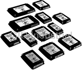
Lambda PH75F Series DC-DC Converters, 200 - 400VDC for 280V Modules & 36 - 76VDC for 48V Modules; 3....
Lambda PXD2024S05N Single Output 20 Watt DC-DC Converter
Request a Quote

The quote request has been received
Close

Facing challenges or have inquiries? Feel free to contact us!
Call Us +1-469-283-2440
What they say about us
FANTASTIC RESOURCE
One of our top priorities is maintaining our business with precision, and we are constantly looking for affiliates that can help us achieve our goal. With the aid of GID Industrial, our obsolete product management has never been more efficient. They have been a great resource to our company, and have quickly become a go-to supplier on our list!
Bucher Emhart Glass
EXCELLENT SERVICE
With our strict fundamentals and high expectations, we were surprised when we came across GID Industrial and their competitive pricing. When we approached them with our issue, they were incredibly confident in being able to provide us with a seamless solution at the best price for us. GID Industrial quickly understood our needs and provided us with excellent service, as well as fully tested product to ensure what we received would be the right fit for our company.
Fuji
HARD TO FIND A BETTER PROVIDER
Our company provides services to aid in the manufacture of technological products, such as semiconductors and flat panel displays, and often searching for distributors of obsolete product we require can waste time and money. Finding GID Industrial proved to be a great asset to our company, with cost effective solutions and superior knowledge on all of their materials, it’d be hard to find a better provider of obsolete or hard to find products.
Applied Materials
CONSISTENTLY DELIVERS QUALITY SOLUTIONS
Over the years, the equipment used in our company becomes discontinued, but they’re still of great use to us and our customers. Once these products are no longer available through the manufacturer, finding a reliable, quick supplier is a necessity, and luckily for us, GID Industrial has provided the most trustworthy, quality solutions to our obsolete component needs.
Nidec Vamco
TERRIFIC RESOURCE
This company has been a terrific help to us (I work for Trican Well Service) in sourcing the Micron Ram Memory we needed for our Siemens computers. Great service! And great pricing! I know when the product is shipping and when it will arrive, all the way through the ordering process.
Trican Well Service
GO TO SOURCE
When I can't find an obsolete part, I first call GID and they'll come up with my parts every time. Great customer service and follow up as well. Scott emails me from time to time to touch base and see if we're having trouble finding something.....which is often with our 25 yr old equipment.
ConAgra Foods