

 Manufacturers
PANASONIC SEMICONDUCTOR SOLUTIONS MN1381-E

Description
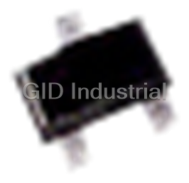
VOLT DETECT IC CMOS 2.2V TO-92
Part Number
MN1381-E
Price
Request Quote
Manufacturer
PANASONIC SEMICONDUCTOR SOLUTIONS
Lead Time
Request Quote
Category
None
Datasheet

Extracted Text
Microcomputer Peripheral LSIs MN1380 Series CMOS LSIs for Voltage Detection Overview Pin Assignment The MN1380 series are elements that monitor the power supply voltage supplied to microcomputers and other LSI systems and issue reset signals for initializing the system after the power is first applied or for preventing runaway 23 operation when the supply voltage fluctuates. MN1380 - R There is a choice of three output types: CMOS output, N-channel open drain output, and inverted CMOS out- put. There are also three package types: M, TO-92, and a mini type for surface mounting. Choose the ideal element for your application from the series' wide selection of detection ranks (17 ranks between 21 3 2.0 and 4.9 volts), output types, and package types. M type package Features Three-pin element requiring no adjustment Wide selection of detection ranks (17 ranks between 2.0 and 4.9 volts) 1381 Highly precise detection voltage 23R Detection voltage with hysteresis characteristic ∆VD = 50 mV for ranks C to K ∆VD = 100 mV for ranks L to U Low current consumption: I = 1µA (typ.) for V DD DD = 5 V Low fluctuation in detection voltage with tempera- 12 3 ture (typ. 1 mV/˚C) TO-92 type package Wide selection of output types: CMOS output, N- channel open drain output, and inverted CMOS output 2 Wide selection of package types: M, TO-92, and a mini type for surface mounting. LCR Applications Battery checkers 1 3 Power outage detectors 1=OUT 2=V DD Level discriminators 3=V SS Memory backup systems Mini type package Microcomputer reset circuits Reset circuits for other electronic circuits SAG00003CEM 1 MN1380 Series Microcomputer Peripheral LSIs MN1380 Series Naming Conventions The MN1380 series offers a wide selection of detection ranks, output types, package types, and packaging. All combinations use the following naming conventions. When ordering, be sure to give the correct part number using these naming conventions. MN13801–R (TA) Winding direction for tape packaging (TA) ...... Tape packaging for TO-92 type package (TX) ...... Embossed tape packing for mini type package (TW) ..... Embossed tape packing for mini type package For further details, see the package specifications. Detection voltage rank (C to U) Output type: Blank ········ CMOS output 1 ················ N-channel open drain output 2 ················ inverted CMOS output Package: 0 ················ M type package 1 ················ TO-92 type package 2 ················ Mini type package Matsushita Electronics Corporation MN1380 series of voltage detection CMOS LSIs with low current consumptions (Example) MN13821–R (TW) Embossed tape packaging R rank (detection voltage of 4.0 to 4.3 V) N-channel open drain output Mini type package MN1380 series of voltage detection CMOS LSIs with low current consumption Minimum Packaging Unit Bulk (M and TO-92 types) ·············· 1,000 Magazine (Mini type) ······················ 50 Taping (Mini and TO-92 types) ······· 3,000 2 Microcomputer Peripheral LSIs MN1380 Series Series Lineup Package Output M type Package TO-92 type Package Mini type Package CMOS output MN1380 MN1381 MN1382 N-channel open drain output MN13801 MN13811 MN13821 Inverted CMOS output MN13802 MN13812 MN13822 Detection Ranks (on Voltage) Detection Voltage for Drop in Power Supply Voltage (V ) Detection Voltage Hysteresis Width (∆VD) DL Rank Unit Unit min max min max C 2.0 2.2 D 2.1 2.3 E 2.2 2.4 V 50 300 mV F 2.3 2.5 G 2.4 2.6 H 2.5 2.7 J 2.6 2.9 V 50 300 mV K 2.8 3.1 L 3.0 3.3 M 3.2 3.5 N 3.4 3.7 P 3.6 3.9 Q 3.8 4.1 V 100 300 mV R 4.0 4.3 S 4.2 4.5 T 4.4 4.7 U 4.6 4.9 3 MN1380 Series Microcomputer Peripheral LSIs Block Diagram 2 V DD Voltage + Reference 1 Comparator – 1 * 1 Level Converter OUT Output Circuit + Comparator Voltage – Reference 2 3 V SS 1 Note * : Circuits vary slightly depending on the output type (CMOS output, N-channel open drain output, or inverted CMOS output) Pin Descriptions Pin No. Symbol Function Description 1 OUT Reset signal output pin 2V Power supply pin DD 3V Ground pin SS 4 Microcomputer Peripheral LSIs MN1380 Series Absolute Maximum Ratings V =0V, Ta=25˚C SS Parameter Symbol Rating Unit Power supply voltage V 7.0 V DD Output voltage V – 0.3 to V +0.3 V O DD Operating ambient temperature Ta –20 to +70 ˚C Storage temperature T –55 to +125 ˚C stg Recommended Operating Conditions V =0V, Ta=25˚C SS Parameter Symbol Conditions min typ max Unit V See Figures 1 and 4. 1.5 6.0 V Power supply DD voltage Electrical Characteristics 1) DC Characteristics V =0V, Ta=–20˚C to +70˚C SS Parameter Symbol Conditions min typ max Unit *1 Power supply current I V = 5 V DD DD 15 µA Load resistance = 10 kW Detection voltage for drop 2 2 * * V V DL *2 in power supply voltage Ta=25˚C Detection voltage hysteresis See Figures 1 and 4. 2 2 * * ∆VD mV *2 width "H" level output voltage V CMOS output I =– 40µA 0.8V V OH OH DD DD Inverted V =1.8V V V DD DD 0.8 CMOS output I =– 0.5mA –1.5 OH "L" level output voltage V N-channel open V =1.8V V 0.4 OL DD SS drain output I =0.7mA OL V Inverted V =6.0V V 0.6 DD SS CMOS output I =0.3mA OH Notes 1 * : This includes the output pin's leakage current. 2 * : For particulars, see the detection voltage rank table. 5 MN1380 Series Microcomputer Peripheral LSIs Electrical Characteristics (continued) 2) AC Characteristics V =0V, Ta=25˚C SS Allowable Value (typ) Parameter Symbol Conditions Unit MN1380 MN13801 MN13802 MN1381 MN13811 MN13812 Rank MN1382 MN13821 MN13822 C D E 3.0 2.5 230.0 F G See H Reset release time t Figures J 3.0 3.0 100.0 µs OH 2 and 3. K L M N P Q 2.0 4.0 30.0 R S T C D E 250.0 160.0 3.0 F G See H Reset time t Figures J 115.0 100.0 3.0 µs OL 2 and 3. K L M N P Q 15.0 35.0 3.0 R S T 6 Microcomputer Peripheral LSIs MN1380 Series Description of Operation V DD V DH V DL 1.5V 0V t CMOS output, N-channel MN1380/1381/1382 open drain output MN13801/13811/13821 V OUT t t OH OH t t OL OL 0V t Inverted CMOS MN13802/13812/13822 output Figure V OUT t OL t OL t t OH OH 0V t Figure 1. Description of Operation Notes 1: Output cannot be specified for power supply voltages under 1.5 V because operation is not guaranteed for that range. 2: V : Detection voltage for drop in power supply voltage DL V : Detection voltage for rise in power supply voltage DH t : Time lag between the time that the power supply voltage reaches the detection voltage (V or V ) and the time that the OL DL DH output pin (OUT) goes to "L" level. t : Time lag between the time that the power supply voltage reaches the detection voltage (V or V ) and the time that OH DL DH the output pin (OUT) goes to "H" level. 3: These characteristics for the N-channel open drain output are when a load resistor is connected between the OUT and V DD pins. 7 MN1380 Series Microcomputer Peripheral LSIs Description for Measuring the Output Characteristics V DD 6.0V 1.6V 0V t 6.0V CMOS output, N-channel open drain output MN1380/1381/1382 MN13801/13811/13821 t OH 1.5V t OL 1.0V 0V t Inverted CMOS output MN13802/13812/13822 6.0V 1.6V t OH 1.5V t OH 1.0V 0V t Figure 2. Description chart of Measuring the Output Characteristics Switch: Connect when measuring 100kΩ N-channel open drain output (MN13801/MN13811/MN13821) V MN1380 Series DD 100pF V OUT Figure 3. Circuit for Measuring the Output Characteristics 8 Microcomputer Peripheral LSIs MN1380 Series Description for Measuring the I/O Characteristics V OUT CMOS output, N-channel open drain output MN1380/1381/1382 MN13801/13811/13821 ∆VD Operation indeterminate 0 0 1.5V V DD V V DL DH V OUT Inverted CMOS output MN13802/13812/13822 ∆VD Operation indeterminate 0 0 1.5V V DD V V DL DH Figure 4. Description chart for Measuring the I/O Characteristics Notes : Output cannot be specified for power supply voltages under 1.5 V because operation is not guaranteed for that range. 1 : V : Detection voltage for drop in power supply voltage 2 DL V : Detection voltage for rise in power supply voltage DH : These characteristics for the N-channel open drain output are when a load resistor is connected between the OUT and V pins. 3 DD 9 MN1380 Series Microcomputer Peripheral LSIs Application Circuit Example Connect resistors, capacitors, and the like only to the output pin on the MN1380 series element. Note that connect- ing them to the Power source pins changes V , V , and ∆VD. DH DL Sample Circuit 1 Sample Circuit 2 V V DD DD R OUT OUT MN1380 MN1380 Series Series C C Select the values of R and C to match the application. 10 Microcomputer Peripheral LSIs MN1380 Series Package Dimensions (Unit: mm) M type package 6.9 1.5 2.5 1.5 1.0 0.7R 0.45±0.1 0.85 0.55±0.1 1.25 2.5±0.5 2.5±0.5 12 3 Note) The package will be changed to lead-free type (M3A). See the new package dimensions section later of this datasheet. 11 1.25 1.25 0.4 1.0 4.1 4.5 MN1380 Series Microcomputer Peripheral LSIs Package Dimensions (Unit: mm)(continued) TO-92 type package 5.0±0.2 4.0±0.2 +0.2 0.45-0.1 2.54±0.15 2.3±0.2 12 3 Note) The package will be changed to lead-free type (SSIP003-P-0000S). See the new package dimensions section later of this datasheet. 12 13.5±0.5 5.1±0.2 Microcomputer Peripheral LSIs MN1380 Series Package Dimensions (Unit: mm)(continued) Mini type package +0.2 -0.3 2.8 +0.25 0.65±0.15 1.5 -0.05 0.65±0.15 0.4±0.2 0.1 to 0.3 Note) The package will be changed to lead-free type (MINI-3DC). See the new package dimensions section later of this datasheet. 13 1.9±0.2 0.5 0.95 0.95 0.5 +0.1 1.45 0.16 -0.05 +0.1 0.4 -0.05 0.8 +0.2 +0.2 0 to 0.1 1.1 -0.1 2.9 -0.05 MN1380 Series Microcomputer Peripheral LSIs Reference Characteristics The following characteristics curves represent results from a specific sample therefore they do not guarantee the characteristics for the final product. 1.4 1.2 1.0 V OUT SS 0.8 V DD 0.6 A 0.4 V 0.2 0 0 1.0 2.0 5.0 7.0 3.0 4.0 6.0 V (V) DD Figure 5.b. Measurement Circuit Figure 5.a. I vs. V Characteristic (Rank Q) DD DD 2.0 V OUT SS 1.5 V DD A 1.0 5V 0.5 –40 –20 0 20 40 60 80 Ambient temperature, Ta (˚C) Figure 6.a. I Temperature Characteristic (Rank Q) Figure 6.b. Measurement Circuit DD 14 I (µA ) DD I (µA ) DD Microcomputer Peripheral LSIs MN1380 Series Reference Characteristics (continued) 4.8 4.6 4.4 V OUT SS 4.2 V DH V DD V 4.0 V DL 3.8 V 3.6 3.4 –40 –20 0 20 40 60 80 Temperature Ta(˚C) Figure 7.a. V /V Temperature Characteristic (Rank Q) Figure 7.b. Measurement Circuit DL DH 0.3 0.25 V OUT SS 0.2 V V DD 0.15 0.1 V 0.05 0 –40 –20 0 2040 6080 Ambient temperature, Ta (˚C) Figure 8.a. ∆VD Temperature Characteristic (Rank Q) Figure 8.b. Measurement Circuit 15 V ,V (V) ∆VD(V) DL DH MN1380 Series Microcomputer Peripheral LSIs Reference Characteristics (continued) 3 –30˚C Room temperature 80˚C V OUT SS 2 V DD A 1 1.8V V 0 0 1.0 1.5 2.0 3.0 0.5 2.5 V (V) OL Figure 9.a. I vs. V Characteristic Figure 9.b. Measurement Circuit OL OL 20 –30˚C Room temperature 15 V OUT SS 80˚C V DD 10 A 5V V 5 0 01 2 3 4 5 V (V) OL Figure 10.a. I vs. V Characteristic Figure 10.b. Measurement Circuit OH OH 16 | I | (mA) OH I (mA) OL Microcomputer Peripheral LSIs MN1380 Series Reference Characteristics (continued) 2.5 2.0 V OUT SS 1.5 V DD A 1.0 1.8V V 0.5 0 –40 –20 020 40 60 80 Ambient temperature, Ta (˚C) Figure 11.a. I vs. Temperature Characteristic Figure 11.b. Measurement Circuit OL 7.0 6.5 V OUT SS 6.0 V DD A 5.5 5V V 5.0 4.5 –40 –20 020 40 60 80 Ambient temperature, Ta (˚C) Figure 12.b. Measurement Circuit Figure 12.a. I vs. Temperature Characteristic OH 17 | I | (mA) OH I (mA) OL MN1380 Series Microcomputer Peripheral LSIs TO-92 Type Package Taping-Specifications (MN1381/MN13811/MN13812) 0 ∆h1 ∆h2 A1 T P1 P d F1 F2 şD0 Drawing direction P0 Figure 13. TO-92 Type Package Taping-Dimensions (Ammunition pack) TO-92 Type Package Taping Dimensions (Ammunition pack) Name Symbol Length (mm) Name Symbol Length (mm) Product height* A 5.3 max Adhesive tape width W0 6.0±0.5 Product width* A1 5.2 max Feed hole position W1 9.0±0.5 Product thickness* T 4.2 max Adhesive tape position W2 0.5 max +0.15 Lead width* d 0.45 Distance to top of product H 25.0 max – 0.1 Taped lead length l1 2.0 max Distance to H0 19.0±0.5 bottom of product Product pitch P 12.7±1.0 Feed hole pitch P0 12.7±0.3 Lead clinch height H1 16.0±0.5 Feed hole position P1 6.35±0.5 Feed hole diameter D0 4.0±0.2 +0.5 Lead spacing F1, F2 2.5 Tape thickness t1 0.7±0.2 – 0.2 Product deflection angle ∆h1, ∆h2 2.0 max Total tape thickness t2 1.5 max +1.0 Tape width W 18.0 – 0.5 1 Note* : For further details, see the specifications issued separately. 25 elements (example) Leave the space for at WH D least three elements 330 250 41 Unit: mm W Figure 14. Box Dimensions for TO-92 Type Packages with Ammunition pack 18 D H0 H A l1 H1 W0 W2 W t2 H E t1 B 2±0.5 Microcomputer Peripheral LSIs MN1380 Series Embossed Taping Specifications for Mini Type Package (MN1382/MN13821/MN13822) There is a choice of two orientations, TW and TX, for the product relative to the tape. TW TX Tape feed hole Tape feed hole Drawing Drawing direction direction (Marking surface on top) (Marking surface on top) Figure 15. TW Orientation Figure 16. TX Orientation Unit: mm +0.1 ş1.5 -0 4.0±0.1 t+0.3±0.1 A B 4.0±0.1 3.2±0.1 Product orientation A is labeled TW; orientation B, TX. Figure 17. Embossed Taping Dimensions for Mini Type Package Unit: mm ş21±0.8 2±0.5 10±1.5 3,000 packages per reel Figure 18. Embossed Taping Reel Dimensions for Mini Type Package 19 8.0±0.3 3.5±0.05 1.75±0.1 ş13±0.5 ş80±1.0 3.3±0.1 1.75±0.1 ş178±2.0 MN1380 Series Microcomputer Peripheral LSIs Reliability Testing Results for MN1380 Series (1) M type package (MN1380/MN13801/MN13802) and TO-92 type package (MN1381/MN13811/MN13812) Test Subjects Test Conditions Results Operating lifetime test V =5.5V, Ta=125˚C, t=1000hrs 0/15 DD High-temperature storage test Ta=150˚C, t=1000hrs 0/15 Low-temperature storage test Ta=–65˚C, t=1000hrs 0/15 High-temperature, Ta=85˚C, RH=85%, t=1000hrs 0/15 high-humidity storage test High-temperature, V =5.5V, Ta=85˚C, RH=85%, t=1000hrs 0/15 DD high-humidity bias test Thermal shock test Ta=150˚C and –65˚C. 0/15 Five minutes at each temperature for ten cycles Temperature cycle test Ta=150˚C and –65˚C. 0/15 Thirty minutes at each temperature for ten cycles Pressure cooker test Two atmospheres for 50 hours at ambient temperature (Ta) of 121˚C 0/15 Soldering test Ambient temperature (Ta) of 230˚C for five seconds 0/15 Solder heat resistance test Ambient temperature (Ta) of 270˚C for ten seconds 0/15 (2) Mini type package (MN1382/MN13821/MN13822) Test Subjects Test Conditions Results Operating lifetime test V =5.5V, Ta=125˚C, t=1000hrs 0/15 DD High-temperature storage test Ta=150˚C, t=1000hrs 0/15 Low-temperature storage test Ta=–65˚C, t=1000hrs 0/15 High-temperature, Ta=85˚C, RH=85%, t=1000hrs 0/15 high-humidity storage test High-temperature, V =5.5V, Ta=85˚C, RH=85%, t=1000hrs 0/15 DD high-humidity bias test Thermal shock test Ta=150˚C and –65˚C. 0/15 Five minutes at each temperature for ten cycles Temperature cycle test Ta=150˚C and –65˚C. 0/15 Thirty minutes at each temperature for ten cycles 1 Pressure cooker test * Two atmospheres for 24 hours at ambient temperature (Ta) of 121˚C 0/15 Soldering test Ambient temperature (Ta) of 230˚C for five seconds 0/15 1 Solder heat resistance test * Ambient temperature (Ta) of 260˚C for five seconds 0/15 1 Note* : Note that the testing conditions for the mini package differ from those for the other two packages. 20 Microcomputer Peripheral LSIs MN1380 Series New Package Dimensions (Unit: mm) • M3A (Lead-free package) 6.90±0.10 2.50±0.10 (1.50) (1.00) (1.50) R0.90 2−R0.70 1 3 +0.10 0.40 -0.05 (0.85) 0.55±0.10 2.50 2.50 21 (0.40) 1.00±0.10 2.25±0.20 2.85±0.20 3.50±0.10 (1.00) 4.10±0.20 4.50±0.10 MN1380 Series Microcomputer Peripheral LSIs New Package Dimensions (Unit: mm)(continued) • SSIP003-P-0000S (Lead-free package) 5.00±0.20 4.00±0.20 0.60±0.15 2.30±0.20 +0.10 0.40 0.40±0.10 -0.05 1 3 1.27 1.27 22 (1.00) (1.00) 5.00±0.20 13.30±0.50 Microcomputer Peripheral LSIs MN1380 Series New Package Dimensions (Unit: mm)(continued) • MINI-3DC (Lead-free package) (1.45) +0.10 0.40 -0.05 2 1 3 0.95 0.95 1.90+0.20 +0.20 2.90 -0.05 Seating plane 0.40±0.20 0.10 to 0.30 23 +0.20 1.10 -0.10 0 to 0.10 +0.25 +0.30 1.50 1.20 (0.65) (0.65) -0.05 -0.10 +0.20 2.80 -0.30 +0.10 0.16 -0.06 Request for your special attention and precautions in using the technical information and semiconductors described in this material (1) An export permit needs to be obtained from the competent authorities of the Japanese Govern- ment if any of the products or technologies described in this material and controlled under the "Foreign Exchange and Foreign Trade Law" is to be exported or taken out of Japan. (2) The technical information described in this material is limited to showing representative character- istics and applied circuit examples of the products. It does not constitute the warranting of industrial property, the granting of relative rights, or the granting of any license. (3) The products described in this material are intended to be used for standard applications or gen- eral electronic equipment (such as office equipment, communications equipment, measuring in- struments and household appliances). Consult our sales staff in advance for information on the following applications: • Special applications (such as for airplanes, aerospace, automobiles, traffic control equipment, combustion equipment, life support systems and safety devices) in which exceptional quality and reliability are required, or if the failure or malfunction of the products may directly jeopardize life or harm the human body. • Any applications other than the standard applications intended. (4) The products and product specifications described in this material are subject to change without notice for reasons of modification and/or improvement. At the final stage of your design, purchas- ing, or use of the products, therefore, ask for the most up-to-date Product Standards in advance to make sure that the latest specifications satisfy your requirements. (5) When designing your equipment, comply with the guaranteed values, in particular those of maxi- mum rating, the range of operating power supply voltage and heat radiation characteristics. Other- wise, we will not be liable for any defect which may arise later in your equipment. Even when the products are used within the guaranteed values, redundant design is recommended, so that such equipment may not violate relevant laws or regulations because of the function of our products. (6) When using products for which dry packing is required, observe the conditions (including shelf life and after-unpacking standby time) agreed upon when specification sheets are individually exchanged. (7) No part of this material may be reprinted or reproduced by any means without written permission from our company. Please read the following notes before using the datasheets A. These materials are intended as a reference to assist customers with the selection of Panasonic semiconductor products best suited to their applications. Due to modification or other reasons, any information contained in this material, such as available product types, technical data, and so on, is subject to change without notice. Customers are advised to contact our semiconductor sales office and obtain the latest information before starting precise technical research and/or purchasing activities. B. Panasonic is endeavoring to continually improve the quality and reliability of these materials but there is always the possibility that further rectifications will be required in the future. Therefore, Panasonic will not assume any liability for any damages arising from any errors etc. that may ap- pear in this material. C. These materials are solely intended for a customer's individual use. Therefore, without the prior written approval of Panasonic, any other use such as reproducing, selling, or distributing this material to a third party, via the Internet or in any other way, is prohibited. 2001 MAR
Frequently asked questions
How does Industrial Trading differ from its competitors?

Is there a warranty for the MN1381-E?
Which carrier will Industrial Trading use to ship my parts?
Can I buy parts from Industrial Trading if I am outside the USA?
Which payment methods does Industrial Trading accept?


What they say about us
FANTASTIC RESOURCE
One of our top priorities is maintaining our business with precision, and we are constantly looking for affiliates that can help us achieve our goal. With the aid of GID Industrial, our obsolete product management has never been more efficient. They have been a great resource to our company, and have quickly become a go-to supplier on our list!
Bucher Emhart Glass
EXCELLENT SERVICE
With our strict fundamentals and high expectations, we were surprised when we came across GID Industrial and their competitive pricing. When we approached them with our issue, they were incredibly confident in being able to provide us with a seamless solution at the best price for us. GID Industrial quickly understood our needs and provided us with excellent service, as well as fully tested product to ensure what we received would be the right fit for our company.
Fuji
HARD TO FIND A BETTER PROVIDER
Our company provides services to aid in the manufacture of technological products, such as semiconductors and flat panel displays, and often searching for distributors of obsolete product we require can waste time and money. Finding GID Industrial proved to be a great asset to our company, with cost effective solutions and superior knowledge on all of their materials, it’d be hard to find a better provider of obsolete or hard to find products.
Applied Materials
CONSISTENTLY DELIVERS QUALITY SOLUTIONS
Over the years, the equipment used in our company becomes discontinued, but they’re still of great use to us and our customers. Once these products are no longer available through the manufacturer, finding a reliable, quick supplier is a necessity, and luckily for us, GID Industrial has provided the most trustworthy, quality solutions to our obsolete component needs.
Nidec Vamco
TERRIFIC RESOURCE
This company has been a terrific help to us (I work for Trican Well Service) in sourcing the Micron Ram Memory we needed for our Siemens computers. Great service! And great pricing! I know when the product is shipping and when it will arrive, all the way through the ordering process.
Trican Well Service
GO TO SOURCE
When I can't find an obsolete part, I first call GID and they'll come up with my parts every time. Great customer service and follow up as well. Scott emails me from time to time to touch base and see if we're having trouble finding something.....which is often with our 25 yr old equipment.
ConAgra Foods