

 Manufacturers
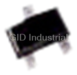
PANASONIC SEMICONDUCTOR SOLUTIONS AN8011S-E1V

Description
IC DC/DC CONVERTER 2CH SO-16
Part Number
AN8011S-E1V
Price
Request Quote
Manufacturer
PANASONIC SEMICONDUCTOR SOLUTIONS
Lead Time
Request Quote
Category
None
Datasheet

Extracted Text
Voltage Regulators AN8011S 2-channel step-down, step-up, or inverting use DC-DC converter control IC Unit: mm � Overview 10.1±0.3 16 9 The AN8011S is a DC-DC converter control IC with two-channel output using the PWM method which allows 500 kHz high-speed control. Respective output operation can be completely synchronized with each other by using the same 0.3 oscillation output. 18 � Features • PWM control frequency of 500 kHz is available. • Wide operating supply voltage range 1.27 0.4 0.40±0.25 (V = 3.6 V to 34 V) CC Seating plane Seating plane • Built-in 2-channel of open collector type for out- put (A single-channel is also usable for inverted SOP016-P-0225A amplification type) • Each output can be stopped independently by the Note) The package of this product will be changed to lead-free type external control . (SOP016-P-0225E). See the new package dimensions section • Built-in on/off function for the operation/stop of later of this datasheet. IC Incorporating circuit for short-circuit protec- tion and under-voltage lock-out (U.V.L.O.) • The latch circuit is externally controllable. • Low consumption current (during operation: 5 mA, during standby: 2 µA) � Applications • LCD displays, digital still cameras, and PDAs � Block Diagram Error amp. Latch V PWM1 REF Unlatch pro. Short pro. U.V.L.O. Unlatch pro. PWM2 OSC On/ Off Error amp. Publication date: December 2001 SDH00002BEB 1 1 16 CT V REF 15 2 Latch RT 14 3 IN+ On/Off 13 4 IN−1 IN−2 12 5 FB1 FB2 11 6 DTC1 DTC2 10 7 Out1 Out2 4.2±0.3 0.1±0.1 1.5±0.2 6.5±0.3 9 8 GND V CC (0.15) AN8011S � Pin Descriptions Pin No. Symbol Description 1 CT Pin for connecting the oscillation frequency setting capacitor for triangular oscillation circuit. Frequency of triangular oscillation is set by connecting a capacitor between this terminal and GND. 2 RT Resistor connection pin for setting the oscillation frequency of triangular oscillation circuit. Frequency of triangular oscillation is set by connecting resistance between the pin and GND 3 On/Off "On/Off" pin for turning on/off IC. "Low" stops IC (output off) and "High" operates IC. 4IN−2 Inverted input pin for channel 2 error amplifier 5 F/B 2 Output pin for channel 2 error amplifier. Gain setting or phase compensation is perfor- med by connecting resistor or capacitor between the pin and IN−2. It is also connected to PWM short-circuit protection. 6 DTC 2 Pin for setting dead-time period of channel 2. The dead-time of channel 2 is set by conn- ecting external resistor. Soft start function can be also given by connecting capacitor in parallel with the external resistor. In addition, only channel 2 output can be turned off by decreasing the pin voltage to below 0.12 V. (short-circuit protection function stop circuit) 7 Out 2 Channel 2 open-collector type output pin. I = 100 mA maximum O 8 GND Grounding pin of signal system. 9V Power supply voltage application pin. It detects start voltage and stop voltages CC 10 Out 1 Channel 1 open-collector type output pin. I = 100 mA maximum O 11 DTC 1 Pin for setting dead-time period of channel 1. The dead-time period of channel 1 is set by connecting external resistor. Soft start function can be also given by connecting capacitor in parallel with the external resistor. In addition, only channel 1 output can be turned off by decreasing the pin voltage to below 0.12 V. (short-circuit protection function stop circuit) 12 F/B 1 Output pin for channel 1 error amplifier. Gain setting or phase compensation is perfor- med by connecting resistor or capacitor between the pin and IN−1. It is also connected to PWM short-circuit protection. 13 IN−1 Inverted input pin for channel 1 error amplifier. 14 IN+ Pin for noninverted input of channel 1 error amplifier. 15 Latch Pin for connecting the time constant setting capacitor for timer latch type short-circuit protection circuit. The time constant for short-circuit protection is set by connecting a capa- citor between this terminal and GND. 16 V Internal reference voltage output pin (2.5 V (allowance: ±3%)). If a load of 20 mA typical REF or more is applied, the overcurrent protection operates to reduce V and switching REF operation stops. SDH00002BEB 2 AN8011S � Absolute Maximum Ratings at T = 25°C a Parameter Symbol Rating Unit Supply voltage V 35 V CC * Power dissipation P 380 mW D Operating ambient temperature T −30 to +85 °C opr Storage temperature T −40 to +125 °C stg Note) 1. Do not apply external currents or voltages to any pins not specifically mentioned. For circuit currents, '+' denotes current flowing into the IC, and '−' denotes current flowing out of the IC. 2 : When using the IC at T of 25°C or more, the power dissipation should be decreased 3.8 mW per 1°C. * a � Recommended Operating Range Parameter Symbol Range Unit Supply voltage V 3.6 to 34 V CC � Electrical Characteristics at V = 12 V, T = 25°C CC a Parameter Symbol Conditions Min Typ Max Unit Reference voltage block Output voltage V 2.413 2.5 2.588 V REF Input regulation with input fluctuation Line V = 3.6 V to 34 V 320 mV CC Load regulation Load I = 0 mA to 5 mA 210 mV REF Output voltage temperature V T = −25°C to + 25°C ±1 % TC1 a * characteristics 1 Output voltage temperature V T = 25°C to 85°C ±1 % TC2 a * characteristics 2 * Overcurrent protection drive current I −20 mA CC U.V.L.O. block Circuit operation start voltage V 2.8 3.1 3.4 V UON Hysteresis width V 100 200 300 mV HYS Error amplifier block 1 Input offset voltage 1 V −6 6mV IN-O1 Input current 1 I −500 −25 100 nA B1 Common-mode input voltage range V 0.5 0.8 V CM High-level output voltage 1 V V − 0.3 V EH1 REF Low-level output voltage 1 V 0.5 V EL1 Error amplifier block 2 Input current 2 I 25 100 nA B2 Common mode input threshold voltage V + 0.72 0.75 0.78 V IN High-level output voltage 2 V V − 0.3 V EH2 REF Low-level output voltage 2 V 0.5 V EL2 SDH00002BEB 3 AN8011S � Electrical Characteristics at V = 12 V, T = 25°C (continued) CC a Parameter Symbol Conditions Min Typ Max Unit PWM comparator 1/2 block High-level input threshold voltage V f = 200 kHz, duty = 100% 1.2 V DT-H OSC Low-level input threshold voltage V f = 200 kHz, duty = 100% 0.6 V DT-L OSC Input current I R = 20 kΩ−37 −34 −31 µA DTC T Output 1/2 block Output frequency 1 f C = 150 pF, R = 20 kΩ, I = 30 mA 180 200 220 kHz OUT1 T T O Frequency 1 f V = 3.6 V to 34 V −2 2% dv CC C = 150 pF, R = 20 kΩ T T Output duty ratio 1 Du C = 150 pF, R = 20 kΩ, R = 24 kΩ 40 45 50 % 1 T T DTC Output duty ratio 2 Du C = 150 pF, R = 20 kΩ, R = 33 kΩ 65 75 85 % 2 T T DTC Output saturation voltage 1 V I = 30 mA 0.9 V O(sat)1 O Output saturation voltage 2 V I = 100 mA 1.2 V O(sat)2 O Output leak current 1 I V = 34 V, when output 10 µA OLe1 CC transistor is off * Frequency temperature characteristics 1 f f = 200 kHz, T = −30°C to +25°C ±9 % dT1 OSC a * Frequency temperature characteristics 2 f f = 200 kHz, T = 25°C to 85°C ±9 % dT2 OSC a * Output frequency 2 f C = 150 pF, R = 6.6 kΩ, I = 30 mA 500 kHz OUT2 T T O * Frequency 2 f V = 3.6 V to 34 V, ±2 % dv2 CC C = 150 pF, R = 6.6 kΩ T T Short-circuit protection block Input threshold voltage V 1.75 1.85 1.95 V SLTH Latch drive voltage V 1.15 1.25 1.35 V SLON Charge current I −120 −50 −40 µA CHG Unlatch pro. 1/2 block Input threshold voltage V 0.12 V ULTH On/off block Threshold voltage V 0.8 2V TH Whole device Total consumption current I V = 12 V, R = 20 kΩ 57 mA CC CC T Total consumption current fluctuation I V = 3.6 V to 34 V, R = 20 kΩ 2mA CC(max.) CC T Standby consumption current I V = 12 V, V is down 2 µA CC(SB) CC REF Maximum standby consumption current I V = 34 V, V is down 5 µA CC(SB-M) CC REF Note) : These characteristics are theoretical values based on the IC design and are not guaranteed. * SDH00002BEB 4 AN8011S � Terminal Equivalent Circuits Pin No. Equivalent circuit Description I/O 1 CT: O V REF 16 The terminal used for connecting a timing capacitor to set oscillator frequency. Use a To PWM input I O capacitance value within the range of 100 pF CT to 0.1 mF. For frequency setting method, OSC 1 comp. refer to the "Application Notes, [2] Function descriptions" section. Use the oscillation fre- 2I O quency in the range of 1 kHz to 500 kHz. 2 RT: I V REF 16 The terminal used for connecting a timing resistor to set oscillation frequency. Use a resistance value ranging from 5.1 kΩ to 20 kΩ. The terminal voltage is 0.67 V typ. OSC PWM RT (= 0.67 V) 2 3 On/Off: I The terminal for on/off control. Internal High-level input: normal operation circuit start/stop On/Off 17 kΩ (V > 2.0 V typ.) ON/OFF 3 Low-level input: standby state 13 kΩ (V < 0.8 V typ.) ON/OFF The total current consumption in the standby state can be suppressed to a value below 5 µA. 4IN−2: I V REF The terminal for the inverted input of ch.2 16 error amplifier. Use a common-mode input ranging from − 0.1 V to 0.8 V. 0.75 V 4 IN−2 SDH00002BEB 5 AN8011S � Terminal Equivalent Circuits (continued) Pin No. Equivalent circuit Description I/O 5 FB2: O V REF 16 The output terminal of ch.2 error amplifier. 25 µA typ. Its source current is −25 µA typ. and sink PWM2 current is 8 mA typ. CT Correct the frequency characteristics of the gain and the phase by connecting a resistor 8 mA and a capacitor between the terminal and typ. IN−2 terminal. 5 FB2 6 DTC2: I 1) Terminal for connecting a resistor and a capacitor for setting the dead-time and the soft start period of ch.2 PWM output. V REF 16 Input current I is determined by the tim- DTC ing resistor RT so that dispersion, and fluc- I DTC2 PWM2 tuation with temperature are suppressed. The CT input current is −35 µA typ. U.V.L.O. output when R = 20 kΩ T V RT I = × 1.04 (A) DTC2 R T 6 DTC2 (V : 0.67 V typ.) RT 2) The ch.2 output can be turned off by reduc- ing the terminal voltage to below 0.12 V. (short-circuit protection function stop) 7 Out2: O V REF 16 The ch.2 open-collector type (Darlington) Out2 output terminal. 7 The absolute maximum rating of output cur- rent is 150 mA. Use with an output current under 100 mA normally. 8 GND: GND pin 8 GND 9V : CC 9 The pin to which supply voltage is applied. V CC Use within an operating supply voltage range of 3.6 V to 34 V. SDH00002BEB 6 AN8011S � Terminal Equivalent Circuits (continued) Pin No. Equivalent circuit Description I/O 10 Out1: O V REF 16 Out1 The ch.1 open collector type (darlington) 10 output terminal. The absolute maximum rating of output cur- rent is 150 mA. Use with an output current of 100 mA or less normally. 11 DTC1: I 1) Terminal for connecting a resistor and a capacitor for setting the dead-time and the soft V start period of ch.1 PWM output. REF 16 Input current I is determined by the tim- DTC I DTC1 ing resistor RT so that dispersion and fluctu- PWM1 CT ation with temperature are suppressed. The U.V.L.O. input current is −35 µA typ, when R = 20 kΩ. output T V RT I = × 1.04 (A) DTC2 R T (V : 0.67 V typ.) 11 DTC1 RT 2) The ch.1 output can be turned off by reduc- ing the terminal voltage to below 0.12 V. (short-circuit protection function stop) 12 FB1: O V REF 16 The output terminal of ch.1 error amplifier. 25 µA typ. Its source current is −25 µA typ. and sink PWM1 current is 8 mA typ. CT Correct the frequency characteristics of the gain and the phase by connecting a resistor 8 mA and a capacitor between the terminal and typ. IN−1 terminal. 12 FB1 13 IN−1: I V REF The terminal for the inverted input of ch.1 error amplifier. Use a common-mode input ranging from − 0.1 V to +0.8 V. 14 IN+:I The terminal for noninverted input of ch.1 13 14 error amplifier. Use a common-mode input IN − 1 IN + ranging from − 0.1 V to +0.8 V. SDH00002BEB 7 AN8011S � Terminal Equivalent Circuits (continued) Pin No. Equivalent circuit Description I/O 15 Latch: O V REF 16 Terminal for connecting the time constant setting capacitor for timer latch short-circuit I CHG protection circuit. The charge current I is CHG 4.2 kΩ Latch about −80 µA. typ. S Q R 1.25 V 30 kΩ typ. typ. 10kΩ typ. 1.25 V 15 Latch typ. 16 V:O REF V CC 9 The output terminal for the reference voltage (2.5 V typ.). V overcurrent REF Use it with a load current of −1 mA or under. detection The terminal has a built-in short-circuit pro- tection circuit, and the short-circuit current Bias to is −20 mA typ. other blocks Use the terminal for setting the reference in- V put of the error amplifier. 16 REF SDH00002BEB 8 AN8011S � Application Notes [1] Main characteristics Reference voltage temperature characteristics Maximum duty ratio temperature characteristics 2.500 54 53 2.495 52 2.490 51 2.485 50 2.480 49 −40 −20 0 20 40 60 80 100 −40 −20 0 20 40 60 80 100 Ambient temperature T (°C) Ambient temperature T (°C) a a Output frequency temperature characteristics DTC pin voltage Output duty ratio 210 100 209 90 208 80 207 70 206 60 205 50 f = 500 kΩ OUT f = 200 kΩ OUT 204 40 203 30 202 20 201 10 200 0 −40 −20 0 20 40 60 80 100 0 0.5 1 1.5 Ambient temperature T (°C) DTC pin voltage (V) a Output frequency characteristics 500 100 R = 10 kΩ T R = 5.1 kΩ T R = 20 kΩ T 10 0 2 3 4 5 10 10 10 10 C (pF) T SDH00002BEB 9 Output frequency f (kHz) Reference voltage V (V) OUT REF Output frequency f (kHz) OUT Maximum duty ratio Du(45) (%) Output duty ratio (%) AN8011S � Application Notes (continued) [2] Function descriptions 1. Reference voltage block This block is composed of the band gap circuit, and outputs the temperature compensated 2.5 V reference voltage to the V terminal. The reference voltage is stabilized when the supply voltage is 3.6 V or higher, and REF used as the operating power supply for the IC inside. It is possible to take out a load current of up to −3 mA. Also, an overcurrent protection circuit is built in for the load, thereby protecting the IC from destruction when V REF terminal is short circuited. 2. Triangular wave oscillation block The triangular wave which swings from the wave peak of approximately 1.4 V to the wave bottom of approximately 0.4 V will be generated by connecting a timing capacitor and a resistor to the CT terminal and RT terminal respectively. The oscillation frequency can be freely decided by the value of C and R connected T T externally. The triangular wave is connected with the inverted input of PWM comparator of the IC inside. 3. Error amplifier block This block detects the output voltage of DC-DC converter, and inputs the signal amplified by the pnp transistor input type differential amplifier to the PWM comparator. The common-mode input voltage range is − 0.1 V to 0.8 V, and is a voltage obtained by dividing the reference voltage with resistors. Also, it is possible to perform the gain setting and the phase compensation arbitrarily by connecting the feedback resistor and the capacitor from the error amplifier output terminal to the inverted input terminal. The output voltage V , if positive, is obtained by connecting the resistor-divided reference voltage to the OUT noninverted input terminal as shown in figure 1. 1), and the output voltage V , if negative, is obtained by OUT connecting to the inverted input terminal as shown in figure 1. 2). The output voltages in each of these cases are given in the following equations. R1 + R2 R3 + R4 V = V × V = − (V − V ) × + V OUT1 IN OUT1 REF IN-1 REF R2 R3 R1 + R2 R2 V = V × V = V × IN+ REF IN−1 REF R2 R1 + R2 V V V OUT1 REF 16 REF 16 R1 R3 R1 R3 Error amp.1 Error amp.1 PWM comparator PWM comparator IN+ 14 IN+ 14 input input IN−1 IN−1 13 13 12 12 R2 R4 R2 R4 R R FB1 FB1 NF NF V OUT1 C C NF NF 1) Positive output 2) Negative output Figure 1. Connection method of error amplifier 1 FB2 5 The output voltage of channel 2 V is OUT2 V OUT2 V : 2.5 V exclusively for positive voltage output, and REF method of connection is as shown in figure 2. R R3 NF C PWM comparator NF Error amp.2 R1 R1 + R2 input V = 0.75 × OUT2 0.75V R2 IN−2 4 R4 R2 Figure 2. Connection method of error amplifier 2 SDH00002BEB 10 AN8011S � Application Notes (continued) [2] Function descriptions (continued) 4. Timer latch short-circuit protection circuit This circuit protects the external main switching devices, switching diodes, choke coils, and etc. from destruction or deterioration if overload or short-circuit of power supply output lasts for a certain time. The timer latch type short-circuit protection circuit detects the output level of each error amplifier, and when the output level of either one or both of the error amplifiers exceeds 1.85 V typical, the timer circuit is actuated, and initiates charging the external capacitor for protection enable. If the output of the error amplifier does not return to a normal voltage range by the time when the voltage of this capacitor reaches 1.25 V, it sets the latch circuit, cuts off the output drive transistor, and sets the dead time to 100%. 5. Low input voltage malfunction prevention circuit (U.V.L.O.) This circuit protects the system from destruction or deterioration due to control malfunction caused by the supply voltage reduction in the transient state of power on or off. The low input voltage malfunction prevention circuit detects the internal reference voltage according to the supply voltage level, and cuts off the output drive transistor by resetting the latch circuit, thereby setting the dead- time to 100% and keeping the latch terminal low. 6. PWM comparator block The PWM comparators, each has one inverted input, and two noninverted inputs, and controls the on-period of output pulse in accordance with the input voltage. It turns on the output transistor during the period when the triangular wave of C terminal is lower than either the error amplifier output voltage or the DTC terminal voltage. T The dead-time is set by the addition of a resistor between the DTC terminal and GND. By the addition of a capacitor in parallel with the external resistor R , the soft start function which gradually extends the on-period DTC of the output pulse by the RC time constant when the power supply is turned on starts to work. 7. Output block The output drive transistor is of open-collector type output connected in Darlington circuit of emitter common GND. The breakdown voltage of the collector output terminal is 34 V and it is possible to obtain up to 100 mA output current. 8. Remote circuit It is possible to switch on/off the IC control by an external control signal. When the on/off terminal voltage is lowered to a value below approximately 0.8 V, the internal reference voltage goes down, thereby the IC control is stopped and the circuit current is decreased to 5 µA or less. When the on/off terminal voltage is increased to a value higher than approximately 2.0 V, the internal reference voltage raises and the control operation is started. [3] The time constant setting method for timer latch type short-circuit protection circuit Figure 3 shows the block diagram of the protection latch circuit. The comparator for short-circuit protection compares the output voltage of error amplifier V with the reference voltage (1.85 V) at all the time. When the load FB conditions of DC-DC converter output is stabilized, there is no fluctuation of error amplifier output, and the short- circuit protection comparator also keeps the balance. At this moment, the switch SW1 will be in the off state, and the latch terminal voltage will be kept at approximately 0.9 V typical. When the load conditions suddenly change, and high-level signal (1.85 V typical of higher) is inputted from the error amplifier to the noninverted input of the short-circuit protection comparator, the short-circuit protection com- parator outputs the high-level signal. This signal turns on the switch SW1, and the charging to the capacitor C S connected externally to the latch terminal is started with a current of 80 µA typical. When the external capacitor C is charged up to approximately 1.25 V typical, the latch circuit is set and the under- S voltage lock-out circuit (U.V.L.O.) is enabled, thereby the output drive transistor is cut off and the dead-time is set to 100%. Once the under-voltage lock-out circuit (U.V.L.O.) is enabled, the latch circuit will not be reset unless the power supply is switched off. SDH00002BEB 11 AN8011S � Application Notes (continued) [3] The time constant setting method for timer latch type short-circuit protection circuit (continued) V REF I CHG 80 µA typ. 5 FB2 SW1 Latch comp. 12 4.2 kΩ typ. FB1 30 kΩ Cut output off typ. SR R 1.25 V typ. 1.85 V Latch U.V.L.O. 10 kΩ typ. 4 Latch C S Figure 3. Short-circuit protection circuit When the power supply is turned on, the output is considered to be short-circuited state, so that the error amplifier output becomes high-level, then SW1 becomes on state and the charging starts. It is necessary to set the external capacitor so as to start up the DC-DC converter output voltage before setting the latch circuit in the later stage. Especially, pay attention to the delay of the start-up time when applying the soft-start. [4] Explanation of unlatch protection circuit operation Figure 4 shows the block diagram of the unlatch protection circuit. It is possible to suppress FB terminal, the error amplifier output terminal of the channel, to low by setting DTC terminal to 0.12 V or less through external signal. Consequently, by controlling the DTC terminal voltage, it is possible to operate only one channel, or to start and stop each channel in any required sequence. 12 5 FB1 FB2 Error amp.1 Error amp.2 14 To PW1 To PW2 4 IN+ IN−2 13 IN−1 I I DTC1 DTC2 11 6 DTC1 DTC2 Unlatch protection Unlatch protection comp.1 comp.2 0.12 V typ. 0.12 V typ. Figure 4. Unlatch protection circuit SDH00002BEB 12 AN8011S � Application Notes (continued) [5] Triangular wave oscillation circuit • Oscillation frequency setting method The waveform of triangular wave oscillation is obtained by charging and discharging of the constant current I O from the external timing capacitor C which is connected to CT terminal. The constant current is set by the externally T attached timing resistor R . T The peak value of the wave V and the trough CTH V = 1.4 V typ. CTH value of the wave V are fixed at approximately 1.4 V CTL typical and 0.4 V typical respectively. The oscillation frequency f is obtained by the OSC following formula; V = 0.4 V typ. CTL t t 1 I 1 2 O f = = OSC t + t 2 × C × (V − V ) Charging Discharging 1 2 T CTH CHL (typ.) V 0.67 RT Where I = 2 × = 2 × O R R T T T Because V − V = 1 V CTH CTL 0.67 Figure 5. Triangular wave oscillation waveform f = [Hz] OSC C × R T T (typ.) The output frequency f is equal to f since it is PWM-controlled. OUT OSC [6] Dead-time (maximum duty) setting method The setting of the dead-time is conducted by adjusting the DTC terminal voltage V as shown in figure 6. Since DTC the DTC terminal provides a constant current output through the resistor R , V is adjusted by attaching the external T DTC resistor R . DTC The output duty ratio Du and the DTC terminal voltage V are expressed by the following formula. When the DTC oscillation frequency f is 200 kHz, the output duty ratio is 0% at V = 0.42 V, and 100% at V = 1.35 V. OSC DTC DTC Pay attention to the peak value and the trough value of triangular wave because the overshoot and undershoot voltages depend on the frequency. C waveform V V T CTH REF V RT V I = × 1.04 [A] DTC waveform DTC DTC I DTC R T PWM V CT CTL t t OFF ON FB Out waveform Off On Off DTC t ON Du = × 100 [%] t + t ON OFF R C (typ.) DTC DTC V −V CTH DTC = × 100 [%] V −V CTH CTL ex.) When f = 200 kHz (R = 20 kΩ, C = 150 pF), OSC T T V = I × R DTC DTC DTC V ≈ 1.4 V (typ.) V ≈0.67 V (typ.) (typ.) CTH RT R DTC V ≈ 0.4 V (typ.) I ≈ 35 µA (typ.) = V × × 1.04 [V] CTL DTL RT R T Figure 6. Dead-time setting method When the capacitor C is added in parallel with the external resistor R , the soft start function gradually extends DTC DTC the on-period of the output pulse when the power supply is turned on. This prevents the overshoot of the DC-DC converter output. SDH00002BEB 13 AN8011S � Application Notes (continued) [7] Timing chart Supply voltage (V ) CC 3.6 V 3.1 V typ. Reference voltage (V ) REF Lock-out release 2.5 V Error amplifier output (FB) 1.83 V Power supply Triangular wave (CT) Latch terminal voltage on 1.3 V 0.9 V 0.40 V 0.03 V High Dead-time voltage (V ) DT Low Output transistor collector waveform (OUT) Soft start operation Maximum duty Figure 7. Operation waveform of PWM comparator 2.5 V Reference voltage (V ) REF Short-circuit protection input threshold level 1.85 V Comparator threshold level 1.4 V DTC terminal voltage Latch terminal voltage 0.9 V Error amplifier output (FB) 0.40 V Triangular wave (CT) High Output transistor collector waveform (OUT) Low High Short-circuit protection comparator t PE output Low Figure 8. Operation waveform of short-circuit protection SDH00002BEB 14 AN8011S � Application Circuit Examples • Application circuit example 1 SBD 23 kΩ 3 V −5 V 7 kΩ 0.01 µF 120 kΩ V CC 7 SBD 3 V 5 V f = 200 kHz Error 25.5 kΩ Duty = 75% amp. Latch V PWM1 Unlatch pro. REF 4.5 kΩ Short pro. U.V.L.O. To pin 4 Unlatch pro. OSC PWM2 On/ Error Off amp. 120 kΩ 0.01 µF SBD 5V 3 V 25.5 kΩ 4.5 kΩ SDH00002BEB 15 6 kΩ 14 kΩ 150 pF V 1 16 REF CT 20 kΩ Latch 2 15 RT 3 14 IN+ On/Off IN−2 4 13 IN−1 FB2 5 12 FB1 0.1 µF 0.1 µF DTC2 6 11 DTC1 33 kΩ 33 kΩ 7 10 Out2 Out1 V GND 8 9 CC AN8011S � Application Circuit Examples • Application circuit example 2 500 Ω V = 7 V IN 3.3 V 0.01 µF 100 Ω 120 kΩ V = 7 V 2.5 V CC 10 µF Error amp. Latch V Unlatch pro. PWM1 REF Short pro. U.V.L.O. Unlatch pro. OSC PWM2 On/ Error Off amp. 120 kΩ 0.01 µF R 500 Ω V = 7 V 5 V CC 25.5 kΩ 0.75 V 4.5 kΩ � New Package Dimensions (Unit: mm) • SOP016-P-0225E (Lead-free package) 10.09±0.20 16 9 (1.05) 0° to 10° 0.50±0.10 1 8 +0.10 (0.60) 1.27 0.40 -0.05 Seating plane Seating plane SDH00002BEB 16 150 pF V REF 1 16 CT 20 kΩ 2 Latch 15 RT On/Off 3 14 IN+ IN−2 4 13 IN−1 FB2 5 12 FB1 0.1 µF 0.1 µF 6 4.30±0.20 DTC2 11 DTC1 0.10±0.10 1.50±0.20 6.40±0.30 33 kΩ 33 kΩ Out2 7 10 Out1 100 Ω V 9 GND 8 CC +0.10 0.15 -0.05 Request for your special attention and precautions in using the technical information and semiconductors described in this material (1) An export permit needs to be obtained from the competent authorities of the Japanese Govern- ment if any of the products or technologies described in this material and controlled under the "Foreign Exchange and Foreign Trade Law" is to be exported or taken out of Japan. (2) The technical information described in this material is limited to showing representative character- istics and applied circuit examples of the products. It does not constitute the warranting of industrial property, the granting of relative rights, or the granting of any license. (3) The products described in this material are intended to be used for standard applications or gen- eral electronic equipment (such as office equipment, communications equipment, measuring in- struments and household appliances). Consult our sales staff in advance for information on the following applications: • Special applications (such as for airplanes, aerospace, automobiles, traffic control equipment, combustion equipment, life support systems and safety devices) in which exceptional quality and reliability are required, or if the failure or malfunction of the products may directly jeopardize life or harm the human body. • Any applications other than the standard applications intended. (4) The products and product specifications described in this material are subject to change without notice for reasons of modification and/or improvement. At the final stage of your design, purchas- ing, or use of the products, therefore, ask for the most up-to-date Product Standards in advance to make sure that the latest specifications satisfy your requirements. (5) When designing your equipment, comply with the guaranteed values, in particular those of maxi- mum rating, the range of operating power supply voltage and heat radiation characteristics. Other- wise, we will not be liable for any defect which may arise later in your equipment. Even when the products are used within the guaranteed values, redundant design is recommended, so that such equipment may not violate relevant laws or regulations because of the function of our products. (6) When using products for which dry packing is required, observe the conditions (including shelf life and after-unpacking standby time) agreed upon when specification sheets are individually exchanged. (7) No part of this material may be reprinted or reproduced by any means without written permission from our company. Please read the following notes before using the datasheets A. These materials are intended as a reference to assist customers with the selection of Panasonic semiconductor products best suited to their applications. Due to modification or other reasons, any information contained in this material, such as available product types, technical data, and so on, is subject to change without notice. Customers are advised to contact our semiconductor sales office and obtain the latest information before starting precise technical research and/or purchasing activities. B. Panasonic is endeavoring to continually improve the quality and reliability of these materials but there is always the possibility that further rectifications will be required in the future. Therefore, Panasonic will not assume any liability for any damages arising from any errors etc. that may ap- pear in this material. C. These materials are solely intended for a customer's individual use. Therefore, without the prior written approval of Panasonic, any other use such as reproducing, selling, or distributing this material to a third party, via the Internet or in any other way, is prohibited. 2001 MAR
Frequently asked questions
How does Industrial Trading differ from its competitors?

Is there a warranty for the AN8011S-E1V?
Which carrier will Industrial Trading use to ship my parts?
Can I buy parts from Industrial Trading if I am outside the USA?
Which payment methods does Industrial Trading accept?


What they say about us
FANTASTIC RESOURCE
One of our top priorities is maintaining our business with precision, and we are constantly looking for affiliates that can help us achieve our goal. With the aid of GID Industrial, our obsolete product management has never been more efficient. They have been a great resource to our company, and have quickly become a go-to supplier on our list!
Bucher Emhart Glass
EXCELLENT SERVICE
With our strict fundamentals and high expectations, we were surprised when we came across GID Industrial and their competitive pricing. When we approached them with our issue, they were incredibly confident in being able to provide us with a seamless solution at the best price for us. GID Industrial quickly understood our needs and provided us with excellent service, as well as fully tested product to ensure what we received would be the right fit for our company.
Fuji
HARD TO FIND A BETTER PROVIDER
Our company provides services to aid in the manufacture of technological products, such as semiconductors and flat panel displays, and often searching for distributors of obsolete product we require can waste time and money. Finding GID Industrial proved to be a great asset to our company, with cost effective solutions and superior knowledge on all of their materials, it’d be hard to find a better provider of obsolete or hard to find products.
Applied Materials
CONSISTENTLY DELIVERS QUALITY SOLUTIONS
Over the years, the equipment used in our company becomes discontinued, but they’re still of great use to us and our customers. Once these products are no longer available through the manufacturer, finding a reliable, quick supplier is a necessity, and luckily for us, GID Industrial has provided the most trustworthy, quality solutions to our obsolete component needs.
Nidec Vamco
TERRIFIC RESOURCE
This company has been a terrific help to us (I work for Trican Well Service) in sourcing the Micron Ram Memory we needed for our Siemens computers. Great service! And great pricing! I know when the product is shipping and when it will arrive, all the way through the ordering process.
Trican Well Service
GO TO SOURCE
When I can't find an obsolete part, I first call GID and they'll come up with my parts every time. Great customer service and follow up as well. Scott emails me from time to time to touch base and see if we're having trouble finding something.....which is often with our 25 yr old equipment.
ConAgra Foods