2-R4.5
2-R2.25
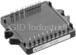
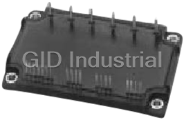
MITSUBISHI SEMICONDUCT MITSUBISHI SEMICONDUCT OR ower Module>
PS11034 PS11034
FLA FLA T-BT ASE TYPE -BASE TYPE
INSULA INSULA TED TYPE TED TYPE
PS11034
INTEGRATED FUNCTIONS AND FEATURES
• Converter bridge for 3 phase AC-to-DC power conversion.
• 3 phase IGBT inverter bridge configured by the latest 3rd.
generation IGBT and diode technology.
O (Note 1):
• Inverter output current capability I
Type Name Motor Rating IO (100%) IO (150%; 60sec)
PS11034 0.75 kW/200V AC 5.0Arms 7.5Arms
(Note 1) : The inverter output current is assumed to be sinu-
soidal and the peak current value of each of the
OP = IO × √ 2,
above loading cases is defined as : I
TC < 100°C
INTEGRATED DRIVE, PROTECTION AND SYSTEM CONTROL FUNCTIONS:
• P-Side IGBTs : Drive circuit, high-level-shift circuit, bootstrap circuit supply scheme for Single Control-Power-Source drive, and un-
der voltage (UV) protection.
• N-Side IGBTs : Drive circuit, DC-Link current sense and amplifier circuits for overcurrent protection, control-supply under-voltage
O) signaling circuit.
protection (UV), and fault output (F
• Fault Output : N-side IGBT short circuit (SC), over-current (OC), and control supply under-voltage (UV).
• Inverter Analog Current Sense : N-Side IGBT DC-Link Current Sense.
• Input Interface : 5V CMOS/TTL compatible, Schmitt Trigger input, and Arm-Shoot-Through interlock protective function.
APPLICATION
Acoustic noise-less 0.75kW/200V AC Class 3 phase inverters, motor control applications,
and motors with built-in small size inverter package
PACKAGE OUTLINES
74±1
60
16.5±0.5
Terminals Assignment :
36
1. CBU+ 21. P1
2. CBU– 22. R
3. CBV+ 23. S
1 2 3 4 5 6 7 8 910 12 14 16
11 4. CBV– 24. T
13 15
3±0.5
0.6
2
5. CBW+ 25. N1
6. CBW– 26. P2
4
7. VD 27. U
8. UP 28. V
9. VP 29. W
10. WP 30. N2
11. UN
12. VN
1.2
5.08 13. WN
14. FO
21 22 23 24 25 26 27 28 29 30
15. Vamp
16. GND
4-R3
45.72
8.5±0.5
(69)
16.5±0.5
22 55.5
Type name,LotNo.
(Fig. 1)
Jan. 2000
63±1
25
15
9
3.5
4.5
(25.7)
25±0.5
50.7±0.8
440 4
0.6 0.4
MITSUBISHI SEMICONDUCTOR
PS11034
FLAT-BASE TYPE
INSULATED TYPE
INTERNAL FUNCTIONS BLOCK DIAGRAM
P1
R
S
T
N1
P2
UV Protection
VD
UP
VP
WP
UN
VN U
WN
V
Fo Circuit
FO
W
V(amp)
+–
N2
GND
(Fig. 2)
MAXIMUM RATINGS (Tj = 25°C)
INVERTER PART
Symbol Item Condition Ratings Unit
VCC Supply voltage Applied between P2-N2 450
V
VCC(surge) Supply voltage (surge) Applied between P2-N2, Surge-value 500 V
VP or VN Each output IGBT collector-emitter static voltage Applied between P2-U.V.W, U.V.W-N2 600 V
VP(S) or Each output IGBT collector-emitter
Applied between P2-U.V.W, U.V.W-N2 600 V
VN(S) switching voltage
±Ic(±Icp) Each output IGBT collector current TC = 25°C, “( )” means IC peak value ±15 (±30) A
CONVERTER PART
Symbol Item Condition Ratings Unit
VRRM 800 V
Repetitive peak reverse voltage
Ea
Recommended AC input voltage 220 Vrms
IO DC output current 3φ rectifying circuit 15 A
IFSM Surge (non-repetitive) forward current 1 cycle at 60Hz, peak value non-repetitive 150 A
2 2 2
I t t for fusing s
I Value for one cycle of surge current 93 A
CONTROL PART
Symbol Item Ratings Unit
VD, VDB Supply voltage
–0.5 ~ 20 V
VCIN
Input signal voltage –0.5 ~ +7.5 V
VFO Fault output supply voltage –0.5 ~ +7.5 V
IFO 15 mA
Fault output current
Iamp
DC-Link IGBT current signal Amp output current 1 mA
Jan. 2000
Input signal conditioning
(Interlock circuit)
OC/SC Protection
UV Protection
Level shifter
Drive circuit Drive circuit
MITSUBISHI SEMICONDUCTOR
PS11034
FLAT-BASE TYPE
INSULATED TYPE
TOTAL SYSTEM
Symbol Condition Ratings Unit
Item
j Junction temperature (Note 2) –20 ~ +125
T °C
Tstg Storage temperature — –40 ~ +125 °C
TC Module case operating temperature (Fig. 3) –20 ~ +100 °C
60 Hz sinusoidal AC applied between all terminals and
VISO Isolation voltage
2500 Vrms
the base plate for 1 minute.
— Mounting torque Mounting screw: M4 0.98 ~ 1.47 N·m
(Note 2) : The indicated values are specified considering the safe operation of all the parts within the ASIPM. The max. ratings for the ASIPM
power chips (IGBT & FWDi) is Tj < 150.
CASE TEMPERATURE MEASUREMENT POINT
TC
(Fig. 3)
THERMAL RESISTANCE
Ratings
Symbol Item Condition Unit
Typ. Max.
Min.
Q Inverter IGBT (1/6)
Rth(jc) — — 2.8 °C/W
Junction to case Thermal
Rth(jc)F Inverter FWDi (1/6) — — 3.9 °C/W
Resistance
Rth(jc)FR Converter Di (1/6) — — 4.8 °C/W
Rth(cf) Contact Thermal Resistance
Case to fin thermal, grease applied (1 Module) — — 0.074 °C/W
ELECTRICAL CHARACTERISTICS (Tj = 25°C, VD = 15V, VDB = 15V unless otherwise noted)
Ratings
Symbol Item
Condition Unit
Min. Typ. Max.
Collector-emitter saturation Tj = 25°C, Input = ON, Ic = 15A, VD = VDB = 15V
VCE(sat) — — 2.9 V
(Shunt voltage drop not included)
voltage
VEC C = 15A
FWDi forward voltage Tj = 25°C, –I — — 2.9 V
VFR Converter diode voltage Tj = 25°C, IFR = 10A — — 1.5 V
IRRM Converter diode reverse current VR = VRRM, Tj = 125°C — — 8 mA
ton
0.3 0.6 1.5 μs
1/2 Bridge inductive, Input = 5V ↔ 0V
tc(on) — 0.5 1.0 μs
VCC = 300V, IC = 15A, Tj = 125°C
Switching times
VD = 15V, VDB = 15V
toff — 1.6 2.5 μs
Note: ton, toff include delay time of the internal control
tc(off) — 0.5 1.3 μs
circuit.
trr FWDi reverse recovery time — 0.12 — μs
Short circuit endurance @VCC ≤ 400V, Input = 5V → 0V (One-Shot) • No destruction
(Output, Arm, and Load Short Circuit Modes) –20°C ≤ Tj (start) ≤ 125°C, 13.5V ≤ VD = VDB ≤ 16.5V • FO output by protection operation
• No destruction
CC ≤ 400V, Input = 5V ↔ 0V, Tj ≤ 125°C
@V
Switching SOA • No protecting operation
IC < OC trip level, 13.5V ≤ VD = VDB ≤ 16.5V
O output
• No F
Jan. 2000
MITSUBISHI SEMICONDUCTOR
PS11034
FLAT-BASE TYPE
INSULATED TYPE
ELECTRICAL CHARACTERISTICS (Tj = 25°C, VD = 15V, VDB = 15V unless otherwise noted)
Ratings
Symbol Item
Condition Unit
Min. Typ. Max.
ID Circuit current (Average) D = 15V, Vin = 5V
Tj = 25°C, V — — 50 mA
IDB Circuit current (Average) Tj = 25°C, VD = VDB = 15V, Vin = 5V — — 5 mA
Vth(on) Input on threshold voltage 0.8 1.4 2.0 V
Vth(off) Input off threshold voltage
2.5 3.0 4.0 V
Ri Input pull-up resistor Applied between input terminal-inside power supply — 50 — kΩ
fPWM PWM input frequency TC ≤ 100°C, Tj ≤ 125°C 1 — 15 kHz
Relates to corresponding inputs
tdead
Arm shoot-through blocking time 2.2 — — μs
TC = –20°C ~ +100°C (Note 3)
tint Input interlock sensing Relates to corresponding input (Fig. 6) — 100 — ns
Vamp(100%) IC = IOP(100%) VD = 15V
Inverter DC-Link IGBT current sense voltage 1.5 2.0 2.5 V
Vamp(200%) output signal IC = IOP(200%) Tj = 25°C (Fig. 4) 3.0 4.0 5.0 V
Vamp(250%) Inverter DC-Link IGBT current sense voltage IC = IOP(250%) VD = 15V 5.0 — — V
C = 0A (Fig. 4)
Vamp(0) output limit I — 50 100 mV
OC Over current trip level Tj = 25°C (Fig. 5) 14.2 17.7 25.0 A
tOC Over current delay time Tj = 25°C (Fig. 5) — 10 — μs
SC
Short circuit trip level Tj = 25°C (Fig. 5) — 30 — A
tSC Short circuit delay time Tj = 25°C (Fig. 5) — 2 — μs
UVD Trip level 11.0 12.0 13.0 V
UVDr
Reset level 11.5 12.5 13.5 V
Supply circuit under
UVDB Trip level TC = Tj = 25°C (Fig. 5) 10.1 10.8 11.6 V
voltage protection
UVDBr 10.6 11.3 12.1 V
Reset level
tdV
Delay time — 10 — μs
tFO Fault output pulse width Tj = 25°C (Note 4) 1.0 1.8 — ms
IFo(H) — — 1 μA
Open collector output (Note 4)
Fault output current
IFo(L)
— — 15 mA
(Note 3) : The dead-time has to be set externally by the CPU; it is not part of the ASIPM internal functions.
(Note 4) : Fault output signaling is given only when the internal OC, SC, & UV protection circuits are activated.
The OC, SC and UV protection (and fault output) operate for the lower arms only. The OC and SC protection Fault output is given
in a pulse format while that of UV protection is maintained throughout the duration of the under-voltage condition.
RECOMMENDED OPERATING CONDITIONS
Ratings
Symbol Item Condition Unit
Min. Typ. Max.
VCC Applied across P2-N2 terminals
Supply voltage — 300 400 V
VD Supply voltage Applied between VD-GND 13.5 15.0 16.5 V
VDB Applied between CBU+ & CBU–, CBV+ & CBV–, CBW+ & CBW–
Supply voltage 13.5 15.0 16.5 V
ΔVD, VDB Supply voltage ripple –1 — +1 V/μs
VCIN(ON) Input on voltage 0 — 0.8 V
Applied between UP • VP • WP • UN • VN • WN and
GND
VCIN(OFF)
Input off voltage 4.0 — 5.0 V
tdead Arm shoot-through blocking time Relates to corresponding inputs 2.2 — — μs
TC Module case operating temperature — — 100 °C
fPWM PWM Input frequency C ≤ 100°C, Tj ≤ 125°C
T — — 15 kHz
tXX Allowable minimum input on-pulse width 1 — — μs
Vamp
5
INVERTER DC-LINK IGBT CURRENT ANALOGUE
VD = 15V
SIGNALING OUTPUT (TYPICAL)
4 Tj = 25°C
Vamp (200%)
3
2
Vamp (100%)
1
(Fig. 4)
0
200 300
0 100
Actual Load Peak Current (%), (IC = IO5 2)
Jan. 2000
Vamp (V)
MITSUBISHI SEMICONDUCTOR
PS11034
FLAT-BASE TYPE
INSULATED TYPE
CURRENT ABNORMALITY PROTECTIVE FUNCTIONS
Protection is achieved by monitoring and filtering the N-side
Ic(A)
DC-Bus current. The over-current protection is activated (after al-
Short circuit trip level
lowing a filtering time of 10 μs) when the line current reaches
SC
250% of the rated load-current IO (rms). Similarly, the short circuit
protection is activated (after allowing a filtering time of 2 μs) when
Over current trip level
the line current reaches twice the rated collector-current (IC).
When a current trip-level is exceeded (OC or SC), all the N-side
IGBTs are intercepted (turned OFF) and a fault-signal is output.
OC
After the fault-signal output duration (1.8 ms - typ.), the intercep-
tion is Reset at the following OFF input signal. However, since the
fault may be repetitive, it is recommended to stop the system after
Collector current
the fault-signal is received and check the fault. The trip-level set-
0
tings described above are summarized in the following figure:
2 10
tw (ms)
(Fig. 5)
ARM-SHOOT-THROUGH INTER-LOCK PROTECTIVE FUNCTION
a1
b4
P-Side Input Signal : VCIN(p) ON
a4
b1
N-Side Input Signal : VCIN(n) ON
a3
b2
P-Side IGBT Gate : VGE(p)
0
a2
b3
N-Side IGBT Gate : VGE(n)
0
(Fig. 6)
Description:
(1) During the ON-State of either of the upper-arm or the lower-arm IGBT, the inter-lock protection circuit blocks any erroneous ON pulses (re-
sulting from input noise) from triggering the other arm IGBT and thus it prevents the arm-shoot-through situation.
(2) When two ON-signals are received for both the upper and the lower arms, the signal received first will be passed to the IGBT and the sec-
ond signal will be blocked. The second signal will be passed to its corresponding IGBT immediately after the first signal is OFF.
Note: This protective function provides no fault signaling output. The Dead-Time has to be set using the micro-controller (CPU).
Operation:
a1. P-side normal ON-signal ⇒ P-side IGBT gate turns ON. b1. N-side normal ON-signal ⇒ N-side IGBT gate turns ON.
a2. N-side erroneous ON-signal ⇒ N-side IGBT gate remains OFF. b2. Simultaneous ON-signals ⇒ P-side IGBT gate remains OFF.
a3. While P-side ON-signal remains ⇒ P-side IGBT gate remains ON. b3. N-side receives OFF-signal ⇒ N-side IGBT gate turns OFF.
a4. N-side normal ON-signal ⇒ N-side IGBT gate turns ON. b4. Immediately after (b3) ⇒ P-side IGBT gate turns ON.
RECOMMENDED I/O INTERFACE CIRCUIT
5V
5V
ASIPM
VD(15V)
5.1kW
R
UP,VP,WP,UN,VN,WN
R
Fo
CPU
10kW
V(amp)
0.1nF
0.1nF
GND(Logic)
(Fig. 7)
Jan. 2000


 Manufacturers


What they say about us
FANTASTIC RESOURCE
One of our top priorities is maintaining our business with precision, and we are constantly looking for affiliates that can help us achieve our goal. With the aid of GID Industrial, our obsolete product management has never been more efficient. They have been a great resource to our company, and have quickly become a go-to supplier on our list!
Bucher Emhart Glass
EXCELLENT SERVICE
With our strict fundamentals and high expectations, we were surprised when we came across GID Industrial and their competitive pricing. When we approached them with our issue, they were incredibly confident in being able to provide us with a seamless solution at the best price for us. GID Industrial quickly understood our needs and provided us with excellent service, as well as fully tested product to ensure what we received would be the right fit for our company.
Fuji
HARD TO FIND A BETTER PROVIDER
Our company provides services to aid in the manufacture of technological products, such as semiconductors and flat panel displays, and often searching for distributors of obsolete product we require can waste time and money. Finding GID Industrial proved to be a great asset to our company, with cost effective solutions and superior knowledge on all of their materials, it’d be hard to find a better provider of obsolete or hard to find products.
Applied Materials
CONSISTENTLY DELIVERS QUALITY SOLUTIONS
Over the years, the equipment used in our company becomes discontinued, but they’re still of great use to us and our customers. Once these products are no longer available through the manufacturer, finding a reliable, quick supplier is a necessity, and luckily for us, GID Industrial has provided the most trustworthy, quality solutions to our obsolete component needs.
Nidec Vamco
TERRIFIC RESOURCE
This company has been a terrific help to us (I work for Trican Well Service) in sourcing the Micron Ram Memory we needed for our Siemens computers. Great service! And great pricing! I know when the product is shipping and when it will arrive, all the way through the ordering process.
Trican Well Service
GO TO SOURCE
When I can't find an obsolete part, I first call GID and they'll come up with my parts every time. Great customer service and follow up as well. Scott emails me from time to time to touch base and see if we're having trouble finding something.....which is often with our 25 yr old equipment.
ConAgra Foods