

 Manufacturers
M-SYSTEMS DiskOnChip G4

Description
M-Systems DiskOnChip G4 128MB (1Gb)/256MB (2Gb) 1.8V Flash Disk with MLC NAND and M-Systems’ x2 Technology
Part Number
DiskOnChip G4
Price
Request Quote
Manufacturer
M-SYSTEMS
Lead Time
Request Quote
Category
DiskOnChip
Datasheet

Extracted Text
DiskOnChip G4 128MB (1Gb)/256MB (2Gb) 1.8V Flash Disk with MLC NAND and M-Systems’ x2 Technology Data Sheet, November 2005 Small form factors: Highlights th 69-ball FBGA 9x12 mm package DiskOnChip G4 is M-Systems' 4 generation of Enhanced performance by implementation the DiskOnChip family of products. Based on of: Multi-Level Cell (MLC) NAND, utilizing DMA support Toshiba’s 90nm MLC NAND Large Block MultiBurst operation flash technology and x2 technology from M- Systems, it is one of the industry’s most Unrivaled data integrity with a robust Error efficient storage solutions. MLC NAND flash Detection Code/Error Correction Code technology provides the smallest die size by (EDC/ECC) tailored for MLC NAND flash storing 2 bits of information in a single memory technology ® cell. x2 technology enables MLC NAND to Maximized flash endurance with TrueFFS achieve highly reliable, high-performance data 6.3.2 (and higher) and code storage with a specially designed error Support for major operating systems (OSs), detection and correction mechanism, optimized including Symbian OS, Microsoft Windows file management, and proprietary algorithms for Mobile, Palm OS, Nucleus, Linux, OSE, enhanced performance. Windows CE, and more. Further cost benefits derive from the Compatible with major CPUs, including cost-effective architecture of DiskOnChip G4, TI OMAP, TI DBB, Intel XScale, Infinion, which includes a boot block that can replace EGold and SGold, ADI 652x, Freescale expensive NOR flash, and incorporates both the MX, and Qualcomm MSMxxxx. flash array and an embedded thin controller in a single die. DiskOnChip G4 provides: Flash disk for both code and data storage Low voltage: 1.8V core and I/O Hardware protection and security-enabling features High capacity: single die - 1Gb (128MB), dual die - 2Gb (256MB) Device cascade capacity: up to 4Gb (512MB) Enhanced Programmable Boot Block enabling eXecute In Place (XIP) functionality using 16-bit interface 1 Data Sheet (Preliminary) Rev. 0.3 92-DS-1105-00 DiskOnChip G4 128MB (1Gb)/256MB (2Gb) 1.8V Performance Boot Capability MultiBurst read: 15 MB/sec 2KB Programmable Boot Block with XIP Sustained read: 9 MB/sec capability to replace boot NOR Sustained write: 2.4 MB/sec Download Engine (DE) for automatic download of boot code from Programmable Access time: Boot Block Normal: 33 nsec Asynchronous Boot mode to boot from Protection & Security-Enabling Features ARM-based CPUs, e.g. XScale, TI OMAP, 16-byte Unique Identification (UID) Freescale MX without the need for external number glue logic 16KByte user-controlled One Time Virtual and Paged RAM boot modes.Enable Programmable (OTP) area booting from DiskOnChip under Secure Two configurable hardware-protected Boot platforms partitions for data and code: Exceptional boot performance with Read-only mode MultiBurst operation and DMA support Write-only mode enhanced by external clock One-Time Write mode (ROM-like) partition Hardware Compatibility Protection key and LOCK# signal Configurable interface: simple NOR-like or Sticky Lock (SLOCK) to lock boot multiplexed address/data interface partition CPU compatibility, including: Protected Bad Block Table ARM-based CPUs Reliability and Data Integrity Texas Instruments OMAP, DBB Hardware- and software-driven, on-the-fly Intel XScale PXAxxx family EDC and ECC algorithms Infinion xGold family Analog Devices (ADI) AD652x 4-bit Error Detection Code/Error Correction family Code (EDC/ECC), based on a patented Freescale MX family combination of BCH and Hamming code Zoran ER4525 algorithms, tailored for MLC NAND flash Renesas SH mobile technology Qualcomm MSMxxxx Guaranteed data integrity after power AMD Alchemy failure Motorola PowerPC™ MPC8xx Transparent bad-block management Hitachi SuperH™ SH-x Dynamic and static wear-leveling Supports 8-, 16- and 32-bit architectures 2 Data Sheet (Preliminary) Rev. 0.3 92-DS-1105-00 DiskOnChip G4 128MB (1Gb)/256MB (2Gb) 1.8V ® TrueFFS Software Power Requirements Full hard-disk read/write emulation for Operating voltage transparent file system management Core, I/O: 1.65 to 1.95V Patented TrueFFS Current Consumption Flash file system management Active mode: Automatic block management Read 4.2mA Data management to maximize the Program 7.4mA limit of typical flash life expectancy Erase 7.4mA Dynamic virtual mapping Deep Power-Down mode: Dynamic and static wear-leveling 10 µA (1Gb/128MB) Programming, duplicating, testing and 20 µA (2Gb/256MB) debugging tools available in source code Capacity and Packaging Operating Environment 128MB (1Gb) capacity (single die): Wide OS support, including: Device cascading option for up to Symbian OS four devices (4Gb) Microsoft Windows Mobile 69-ball FBGA package: 9x12x1.2 mm (width x length x Palm OS Nucleus height) Windows CE Ballout compatible with Linux DiskOnChip G3/P3, G3/P3 LP and OSE H1 FBGA products VxWorks 256MB (2Gb) capacity (dual die): TrueFFS Software Development Kit (SDK) Device cascading option for up to for quick and easy support for proprietary two devices (4Gb) OSs, or OS-less environment 69-ball FBGA package: 9x12x1.4 mm (width x length x TrueFFS Boot Software Development Kit height) (BDK) Ballout compatible with DiskOnChip G3/P3, G3/P3 LP, H1 and, H3 FBGA products 3 Data Sheet (Preliminary) Rev. 0.3 92-DS-1105-00 DiskOnChip G4 128MB (1Gb)/256MB (2Gb) 1.8V REVISION HISTORY Doc. No Revision Date Description Reference 92-DT-0305-00 0.1 March 2005 Preliminary version - 0.2 October 2005 Device ball number was reduced Section 2 from 115 to 69 balls (only not connected balls were reduced). Updated mechanical dimensions. Section 10.4 Updated Ordering Information. Section 11 92-DS-1105-00 0.3 November Updated electrical information - 4 Data Sheet (Preliminary) Rev. 0.3 92-DS-1105-00 DiskOnChip G4 128MB (1Gb)/256MB (2Gb) 1.8V TABLE OF CONTENTS 1. Introduction ............................................................................................................................... 9 2. Product Overview.................................................................................................................... 10 2.1 Product Description .......................................................................................................... 10 2.2 Standard Interface............................................................................................................ 11 2.2.1 Ball Diagrams ..................................................................................................................... 11 2.2.2 System Interface ................................................................................................................12 2.2.3 Signal Description ..............................................................................................................13 2.3 Multiplexed Interface ........................................................................................................ 15 2.3.1 Ball Diagram....................................................................................................................... 15 2.3.2 System Interface ................................................................................................................16 2.3.3 Signal Description ..............................................................................................................17 3. Theory of Operation ................................................................................................................ 19 3.1 Overview........................................................................................................................... 19 3.2 System Interface...............................................................................................................20 3.2.1 Standard (NOR-Like) Interface........................................................................................... 20 3.2.2 Multiplexed Interface .......................................................................................................... 20 3.3 Configuration Interface ..................................................................................................... 20 3.4 Protection and Security-Enabling Features...................................................................... 21 3.4.1 Read/Write Protection ........................................................................................................ 21 3.4.2 Unique Identification (UID) Number ................................................................................... 21 3.4.3 One-Time Programmable (OTP) Area ............................................................................... 21 3.4.4 One-Time Write (ROM-Like) Partition ................................................................................ 22 3.4.5 Sticky Lock (SLOCK).......................................................................................................... 22 3.5 Programmable Boot Block with eXecute In Place (XIP) Functionality.............................. 22 3.6 Download Engine (DE)..................................................................................................... 22 3.7 Error Detection Code/Error Correction Code (EDC/ECC) ................................................ 23 3.8 Control and Status............................................................................................................ 23 3.9 Flash Architecture.............................................................................................................23 4. x2 Technology ......................................................................................................................... 25 4.1 MultiBurst Operation......................................................................................................... 25 4.2 DMA Operation................................................................................................................. 28 4.3 Combined MultiBurst Mode and DMA Operation ............................................................. 29 5. Hardware Protection ............................................................................................................... 30 5 Data Sheet (Preliminary) Rev. 0.3 92-DS-1105-00 DiskOnChip G4 128MB (1Gb)/256MB (2Gb) 1.8V 5.1 Method of Operation......................................................................................................... 30 6. Modes of Operation................................................................................................................. 31 6.1 Normal Mode....................................................................................................................32 6.2 Reset Mode ......................................................................................................................32 6.3 Deep Power-Down Mode ................................................................................................. 32 6.4 TrueFFS Technology........................................................................................................ 33 6.4.1 General Description............................................................................................................ 33 6.4.2 Built-In Operating System Support..................................................................................... 34 6.4.3 TrueFFS Software Development Kit (SDK)........................................................................ 34 6.4.4 File Management................................................................................................................ 34 6.4.5 Bad-Block Management..................................................................................................... 34 6.4.6 Wear-Leveling .................................................................................................................... 34 6.4.7 Power Failure Management ............................................................................................... 35 6.4.8 Error Detection/Correction.................................................................................................. 36 6.4.9 Special Features Through I/O Control (IOCTL) Mechanism.............................................. 36 6.4.10 Compatibility....................................................................................................................... 36 6.5 8KB Memory Window....................................................................................................... 36 7. Register Descriptions ............................................................................................................. 38 7.1 Definition of Terms ........................................................................................................... 38 7.2 Reset Values ....................................................................................................................39 7.3 RAM Page Command Register ........................................................................................ 39 7.4 RAM Page Select Register............................................................................................... 39 7.5 Paged RAM COTP Status Download Register....................... Error! Bookmark not defined. 7.6 Paged RAM COTP Select Register........................................ Error! Bookmark not defined. 7.7 Paged RAM Unique ID Download Register...................................................................... 40 7.8 No Operation (NOP) Register........................................................................................... 40 7.9 Chip Identification (ID) Register [0:1]................................................................................ 40 7.10 Test Register .................................................................................................................... 41 7.11 Endian Control Register ................................................................................................... 41 7.12 DiskOnChip Control Register/Control Confirmation Register........................................... 42 7.13 Device ID Select Register................................................................................................. 43 7.14 Configuration Register...................................................................................................... 43 7.15 Interrupt Control Register ................................................................................................. 44 7.16 Interrupt Status Register................................................................................................... 45 7.17 Output Control Register.................................................................................................... 45 6 Data Sheet (Preliminary) Rev. 0.3 92-DS-1105-00 DiskOnChip G4 128MB (1Gb)/256MB (2Gb) 1.8V 7.18 DPD Control Register....................................................................................................... 46 7.19 DMA Control Register [1:0]............................................................................................... 47 7.20 MultiBurst Mode Control Register..................................................................................... 48 7.21 Virtual/Paged RAM Status Register ................................................................................. 49 8. Booting from DiskOnChip G4................................................................................................. 51 8.1 Introduction....................................................................................................................... 51 8.2 Boot Replacement............................................................................................................ 51 8.2.1 Asynchronous Boot Mode .................................................................................................. 51 8.2.2 Virtual RAM Boot................................................................................................................51 8.2.3 Paged RAM Boot................................................................................................................ 52 9. Design Considerations ...........................................................................................................53 9.1 General Guidelines........................................................................................................... 53 9.2 Standard NOR-Like Interface ........................................................................................... 54 9.3 Multiplexed Interface ........................................................................................................ 56 9.4 Connecting Control Signals.............................................................................................. 56 9.4.1 Standard Interface..............................................................................................................56 9.4.2 Multiplexed Interface .......................................................................................................... 57 9.5 Implementing the Interrupt Mechanism ............................................................................ 58 9.5.1 Hardware Configuration ..................................................................................................... 58 9.5.2 Software Configuration....................................................................................................... 58 9.6 Device Cascading............................................................................................................. 59 9.7 Boot Replacement............................................................................................................ 60 9.8 Platform-Specific Issues................................................................................................... 61 9.8.1 Wait State........................................................................................................................... 61 9.8.2 Big and Little Endian Systems............................................................................................ 61 9.8.3 Busy Signal......................................................................................................................... 61 9.8.4 Working with 8/16/32-Bit Systems...................................................................................... 61 9.9 Design Environment ......................................................................................................... 63 10. Product Specifications ........................................................................................................... 64 10.1 Environmental Specifications ........................................................................................... 64 10.1.1 Operating Temperature...................................................................................................... 64 10.1.2 Thermal Characteristics ..................................................................................................... 64 10.1.3 Humidity.............................................................................................................................. 64 10.1.4 Endurance ................................................................................ Error! Bookmark not defined. 10.2 Electrical Specifications.................................................................................................... 64 10.2.1 Absolute Maximum Ratings................................................................................................ 64 7 Data Sheet (Preliminary) Rev. 0.3 92-DS-1105-00 DiskOnChip G4 128MB (1Gb)/256MB (2Gb) 1.8V 10.2.2 Capacitance........................................................................................................................ 64 10.2.3 DC Electrical Characteristics over Operating Range ......................................................... 65 10.2.4 AC Operating Conditions.................................................................................................... 67 10.3 Timing Specifications........................................................................................................ 68 10.3.1 Read Cycle Timing Standard Interface .............................................................................. 68 10.3.2 Write Cycle Timing Standard Interface .............................................................................. 71 10.3.3 Read Cycle Timing Multiplexed Interface........................................................................... 72 10.3.4 Write Cycle Timing Multiplexed Interface........................................................................... 74 10.3.5 Read Cycle Timing MultiBurst............................................................................................ 76 10.3.6 Flash Characteristics.......................................................................................................... 78 10.3.7 Power Supply Sequence.................................................................................................... 78 10.3.8 Power-Up Timing................................................................................................................ 79 10.3.9 Interrupt Timing .................................................................................................................. 81 10.3.10 DMA Request Timing ......................................................................................................... 81 10.4 Mechanical Dimensions.................................................................................................... 83 11. Ordering Information............................................................................................................... 84 How to Contact Us ........................................................................................................................ 85 8 Data Sheet (Preliminary) Rev. 0.3 92-DS-1105-00 DiskOnChip G4 128MB (1Gb)/256MB (2Gb) 1.8V 1. INTRODUCTION This data sheet includes the following sections: Section 1: Overview of data sheet contents Section 2: Product overview, including a brief product description, ball diagrams and signal descriptions Section 3: Theory of operation for the major building blocks Section 4: Major features and benefits of x2 technology Section 5: Detailed description of hardware protection and security-enabling features Section 6: Detailed description of modes of operation and TrueFFS technology, including power failure management and 8KByte memory window Section 7: DiskOnChip G4 register descriptions Section 8: Overview of how to boot from DiskOnChip G4 Section 9: Hardware and software design considerations Section 10: Environmental, electrical, timing and product specifications Section 11: Information on ordering DiskOnChip G4 For additional information on M-Systems’ flash disk products, please contact one of the offices listed on the back page. 9 Data Sheet (Preliminary) Rev. 0.3 92-DS-1105-00 DiskOnChip G4 128MB (1Gb)/256MB (2Gb) 1.8V 2. PRODUCT OVERVIEW 2.1 Product Description DiskOnChip G4 is the latest addition to M-Systems’ DiskOnChip product family. DiskOnChip G4, packed in a small FBGA package with 128MB (1Gb) capacity, is a single-die device with an embedded thin flash controller and flash memory. It uses Toshiba’s cutting-edge, 90nm NAND- based Multi-Level Cell (MLC) large block flash technology, enhanced by M-Systems’ proprietary x2 technology. A dual-die device is available with a single chip capacity of 256MB (2Gb). MLC NAND technology enables two bits of data to be stored on a single cell, cutting in half the physical die size. M-Systems’ proprietary x2 technology overcomes MLC-related error patterns and slow transfer rates by using a robust error detection and correction (EDC/ECC) mechanism. Furthermore, it provides performance enhancement with multi-plane operation, DMA support, turbo operation and MultiBurst operation. The combination of MLC and x2 technology results in a low- cost, minimal-sized flash disk that achieves unsurpassed reliability levels and enhanced performance. This breakthrough in performance, size and cost makes DiskOnChip G4 the ideal solution for product manufacturers who require high-capacity, small size, high-performance, and above all, high-reliability storage to enable applications such as Digital TVs (DTVs), rugged handheld terminals, Digital Still Cameras (DSCs), Mobile Point of Sale (POS), telecom equipment, multimedia phones, camera and Video on Demand (VOD) phones, MP3 phones, enhanced Multimedia Messaging Service (MMS), gaming, video and Personal Information Management (PIM) on mobile handsets, and Personal Digital Assistants (PDAs). As with the DiskOnChip G3, DiskOnChip G4 content protection and security-enabling features offer several benefits. Two write- and read-protected partitions, with both software- and hardware- based protection, can be configured independently for maximum design flexibility. The 16-byte Unique ID (UID) identifies each flash device, eliminating the need for a separate ID device on the motherboard. The 16KB One Time Programmable (OTP) area is written to once and then locked to prevent data and code from being altered, is ideal for storing customer and product-specific information. DiskOnChip G4 has a 2KB Programmable Boot Block. This block provides eXecute In Place (XIP) functionality, enabling DiskOnChip G4 to replace the boot device and function as the only non-volatile memory device on-board. Eliminating the need for an additional boot device reduces hardware expenditures, board real estate, programming time, and logistics. M-Systems’ patented TrueFFS software technology fully emulates a hard disk to manage the files stored on DiskOnChip G4. This transparent file system management enables read/write operations that are identical to a standard, sector-based hard disk. In addition, TrueFFS employs patented methods, such as virtual mapping, dynamic and static wear-leveling, and automatic block management to ensure high data reliability and to maximize flash life expectancy. 10 Data Sheet (Preliminary) Rev. 0.3 92-DS-1105-00 DiskOnChip G4 128MB (1Gb)/256MB (2Gb) 1.8V 2.2 Standard Interface 2.2.1 Ball Diagrams See Figure 1 for the DiskOnChip G4 128MB (1Gb)/256MB (2Gb) ballout for the standard interface. To ensure proper device functionality, balls marked RSRVD are reserved for future use and should not be connected. Note: Fourth-generation DiskOnChip G4 is designed as a drop-in replacement for all DiskOnChip products. assuming that the latter were integrated according to migration guide guidelines. Refer to the DiskOnChip G3/P3 to G3/P3 LP, G4/P4, H1 to DiskOnChip H3 migration guide for further information. 9x12 FBGA Package 12 3 4 5 6 7 8 910 NC NC A NC NC B C NC A7 RSRVD RSRVD WE# A8 A11 A3 A6 RSRVD RSTIN# RSRVD RSRVD A12 RSRVD D A2 A5 NC BUSY# RSRVD A9 LOCK# RSRVD E NC A1 A4 IF_CFG A10 ID0 IRQ# NC F A0/DPD VSS DMARQ# NC D1 D6 ID1 NC G CE# OE# D9 D3 D4 D13 D15 RSRVD H RSRVD D0 D10 VCC VCCQ D12 D7 VSS J D8 D2 D11 D5 D14 CLK K NC NC L NC NC M Figure 1: 9x12 FBGA Ballout for Standard Interface 11 Data Sheet (Preliminary) Rev. 0.3 92-DS-1105-00 DiskOnChip G4 128MB (1Gb)/256MB (2Gb) 1.8V 2.2.2 System Interface See Figure 2 for a simplified I/O diagram for a standard interface of DiskOnChip G4 128MB (1Gb) and 256MB (2Gb). BUSY# CE#. OE#, WE# RSTIN# CLK A] [12:0 DiskOnChip G4 DMARQ# IRQ# D[ [15:0 DPD IF_CFG ID[1:0] LOCK# System Interface Control Configuration Figure 2: Standard Interface Simplified I/O Diagram 12 Data Sheet (Preliminary) Rev. 0.3 92-DS-1105-00 DiskOnChip G4 128MB (1Gb)/256MB (2Gb) 1.8V 2.2.3 Signal Description DiskOnChip G4 FBGA related ball designations are listed in the signal descriptions, presented in logic groups, in Table 1. Table 1: Signal Descriptions for Standard Interface Input Signal Ball No. Description Signal Type 1 Type System Interface A[12:11] D8, C8 ST Address bus. A0 is multiplexed with the DPD ball. Input A[10:8] F7, E7, C7 A[7:4] C3, D3, E3, F3 A[3:0] D2, E2, F2, G2 D[15:14] H8, K8 ST, R8 Data bus, high byte. Not used and may be left Input/ D[13:12] H7, J7 floating when IF_CFG is set to 0 (8-bit mode). Output D[11:8] K5, J4, H4, K3 D[7:6] J8, G7 ST Data bus, low byte. Input/ D[5:3] K7, H6, H5 Output D[2:0] K4, G4, J3 CE# H2 ST Chip Enable, active low. Input OE# H3 ST Output Enable, active low. Input WE# C6 ST Write Enable, active low. Input Configuration ID[1:0] G9, F8 ST Identification. Configuration control. Input DiskOnChip G4 128MB(1Gb) supports up to four chips cascaded in the same memory window: Chip 1 = ID1, ID0 = VSS, VSS (0,0); must be used for single chip configuration. Chip 2 = ID1, ID0 = VSS, VCCQ (0,1) Chip 3 = ID1, ID0 = VCCQ, VSS (1,0) Chip 4 = ID1, ID0 = VCCQ, VCCQ (1,1) DiskOnChip G4 256MB(2Gb) supports up to two chips cascaded in the same memory window: Chip 1 = ID1, ID0 = VSS, VSS (0,0); must be used for single chip configuration Chip 2 = ID1, ID0 = VCCQ, VCCQ (1,1) LOCK# E8 ST Lock, active low. When active, provides full Input hardware data protection of selected partitions. IF_CFG F4 ST Interface Configuration, 1 (VCCQ) for 16-bit Input interface mode, 0 (VSS) for 8-bit interface mode. 13 Data Sheet (Preliminary) Rev. 0.3 92-DS-1105-00 DiskOnChip G4 128MB (1Gb)/256MB (2Gb) 1.8V Input Signal Ball No. Description Signal Type 1 Type Control BUSY# E5 OD Busy, active low, open drain. Indicates that Output DiskOnChip is initializing and should not be accessed. A 10 KΩ pull-up resistor is required if this ball drives an input. A 10 KΩ pull-up resistor is recommended even if this ball is not used. RSTIN# D5 ST Reset, active low. Input CLK K6 ST System Clock. Input DMARQ# G8 OD DMA Request, active low. A 10 KΩ pull-up resistor is Output required if this ball drives an input. A 10 KΩ pull-up resistor is recommended even if this ball is not used. IRQ# F9 OD Interrupt Request, active low. A 10 KΩ pull-up Output resistor is required if this ball drives an input. A 10 KΩ pull-up resistor is recommended even if this ball is not used. DPD G2 ST Deep Power-Down. Used to enter and exit Deep Input Power-Down mode. This ball is assigned A0 instead of DPD when working in 8-bit mode. Power VCC J5 - Device supply. Requires a 10 nF and 0.1 µF Supply capacitor. VCCQ J6 - I/O power supply. Sets the logic 1 voltage level Supply range of I/O balls. VCCQ may be 1.65V to 1.95V. Requires a 10 nF and 0.1 µF capacitor. VSS G3, J9 - Ground. All VSS balls must be connected. Supply Other RSRVD See Figure 1 - Reserved. Other reserved signals are not connected internally and must be left floating to guarantee forward compatibility with future products. M - Mechanical. These balls are for mechanical placement, and are not connected internally. 1. The following abbreviations are used: IN - Standard (non-Schmidt) input, ST - Schmidt Trigger input, OD - Open drain output, R8 - Nominal 22K pull-up resistor, enabled only for 8-bit interface mode (IF_CFG input is 0) 14 Data Sheet (Preliminary) Rev. 0.3 92-DS-1105-00 DiskOnChip G4 128MB (1Gb)/256MB (2Gb) 1.8V 2.3 Multiplexed Interface 2.3.1 Ball Diagram See Figure 3 for the DiskOnChip G4 ballout for the multiplexed interface. To ensure proper device functionality, balls marked RSRVD are reserved for future use and should not be connected. Note: Forth-generation DiskOnChip G4 is designed as a drop-in replacement for all DiskOnChip products, assuming that the latter were integrated according to migration guide guidelines. Refer to the DiskOnChip G3/P3 to G3/P3 LP, G4/P4, H1 to DiskOnChip H3 migration guide for further information. 9x12 FBGA Package 12 3 4 5 6 78 910 A NC NC NC B NC C NC VSS RSRVD RSRVD WE# VSS VSS VSS VSS RSRVD RSTIN# RSRVD RSRVD VSS RSRVD D VSS VSS NC BUSY# RSRVD VSS LOCK# RSRVD E NC VSS VSS VCCQ VSS ID0 IRQ# NC F NC DPD VSS AD1 AD6 DMARQ# AVD# NC G CE# OE# AD9 AD3 AD4 AD13 AD15 RSRVD H AD0 AD10 VCC VCCQ AD12 AD7 VSS RSRVD J AD8 AD2 AD11 CLK AD5 AD14 K NC NC L NC NC M Figure 3 Ballout for Multiplexed Interface 15 Data Sheet (Preliminary) Rev. 0.3 92-DS-1105-00 DiskOnChip G4 128MB (1Gb)/256MB (2Gb) 1.8V 2.3.2 System Interface See Figure 4 for a simplified I/O diagram of DiskOnChip G4. BUSY# RSTIN# CE OC ,# WE# ,# CLK DiskOnChip G 4 DMARQ# AD[15:0] IRQ# DPD ID0 AVD# LOCK# System Interface Configuration Control Figure 4: Multiplexed Interface Simplified I/O Diagram 16 Data Sheet (Preliminary) Rev. 0.3 92-DS-1105-00 DiskOnChip G4 128MB (1Gb)/256MB (2Gb) 1.8V 2.3.3 Signal Description DiskOnChip G4 FBGA related ball designations are listed in the signal descriptions, presented in logic groups, in Table 2. Table 2: Signal Descriptions for Multiplexed Interface Signal Input Signal Pin No. Description 1 Type Type System Interface AD[15:14] H8, K8 ST Multiplexed bus. Address and data signals Input/ Output AD[13:12] H7, J7 AD[11:9] K5, J4, H4 AD[8:6] K3, J8, G7 AD[5:3] K7, H6, H5 AD[2:0] K4, G4, J3 CE# H2 ST Chip Enable, active low Input OE# H3 ST Write Enable, active low Input WE# C6 ST Output Enable, active low Input Configuration AVD# G9 ST Address Valid. Set multiplexed interface Input ID0 F8 ST Identification. Configuration control to support up to two chips Input cascaded in the same memory window. Chip 1 = ID0 = VSS; must be used for single-chip configuration Chip 2 = ID0 = VCC LOCK# E8 ST Lock, active low. When active, provides full hardware data Input protection of selected partitions. Control BUSY# E5 OD Busy, active low, open drain. Indicates that DiskOnChip is Output initializing and should not be accessed A 10 KΩ pull-up resistor is required if this ball drives an input. A 10 KΩ pull-up resistor is recommended even if this ball is not used. RSTIN# D5 ST Reset, active low. Input CLK K6 ST System Clock. Input DMARQ# G8 OD Output DMA Request, active low. A 10 KΩ pull-up resistor is required if this ball drives an input. A 10 KΩ pull-up resistor is recommended even if this ball is not used. IRQ# F9 OD Interrupt Request, active low. A 10 KΩ pull-up resistor is Output required if this ball drives an input. A 10 KΩ pull-up resistor is recommended even if this ball is not used. 17 Data Sheet (Preliminary) Rev. 0.3 92-DS-1105-00 DiskOnChip G4 128MB (1Gb)/256MB (2Gb) 1.8V Input Signal Signal Pin No. Description 1 Type Type DPD G2 ST Deep Power-Down. Used to enter and exit Deep Power- Input Down mode. Pin is assigned A0 instead of DPD when working in 8-bit mode. Power VCC J5 - Device core supply. Requires a 10 nF and 0.1 µF capacitor. Supply VCCQ J6, F4 - I/O power supply. Sets the logic 1 voltage level range of I/O Supply balls. VCCQ may be 1.65V to 1.95V. Requires a 10 nF and 0.1 µF capacitor. VSS G3, J9, D8, - Ground. All VSS pins must be connected. Supply C8, F7, E7, C7, C3, D3, E3, F3, D2, E2, F2 Other RSRVD See Figure 3 - Reserved. Reserved signals are not connected internally and must be left floating to guarantee forward compatibility with future products. M Mechanical. These balls are for mechanical placement, and are not connected internally. 1. The following abbreviations are used: IN - Standard (non-Schmidt) input, ST - Schmidt Trigger input, OD - Open drain output 18 Data Sheet (Preliminary) Rev. 0.3 92-DS-1105-00 DiskOnChip G4 128MB (1Gb)/256MB (2Gb) 1.8V 3. THEORY OF OPERATION 3.1 Overview DiskOnChip G4 consists of the following major functional blocks, as shown in Figure 5. *ADDR[0] and DPD are multiplexed on the same ball/pin. Figure 5: Simplified Block Diagram, Standard Interface These components are described briefly below and in more detail in the following sections. • System Interface for the host interface. • Configuration Interface for configuring DiskOnChip G4 to operate in 8-bit, 16-bit mode, cascaded configuration, hardware read/write protection and entering/exiting Deep Power- Down mode. • Read/Write Protection and OTP for advanced data/code security and protection. • Programmable Boot Block with XIP functionality enhanced with a Download Engine (DE) for system initialization capability. • Error Detection and Error Correction Code (EDC/ECC) for on-the-fly error handling. • Data Pipeline through which the data flows from the system to the NAND flash arrays. • Control & Status block that contains registers responsible for transferring the address, data and control information between the TrueFFS driver and the flash media. • Flash Interface that interfaces to two NAND flash planes. • Bus Control for translating the host bus address, and data and control signals into valid NAND flash signals. • Address Decoder to enable the relevant unit inside the DiskOnChip controller, according to the address range received from the system interface. 19 Data Sheet (Preliminary) Rev. 0.3 92-DS-1105-00 DiskOnChip G4 128MB (1Gb)/256MB (2Gb) 1.8V 3.2 System Interface 3.2.1 Standard (NOR-Like) Interface The system interface block provides an easy-to-integrate NOR-like (also SRAM and EEPROM- like) interface to DiskOnChip G4 enabling it to interface with various CPU interfaces, such as a local bus, ISA bus, NOR interface, SRAM interface, EEPROM interface or any other compatible interface. In addition, the EEPROM-like interface enables direct access to the Programmable Boot Block to permit XIP (Execute-In-Place) functionality during system initialization. A 13-bit wide address bus enables access to the DiskOnChip G4 8KB memory window (as shown in Section 6.5). The Chip Enable (CE#), Write Enable (WE#) and Output Enable (OE#) signals trigger read and write cycles. A write cycle occurs while both the CE# and the WE# inputs are asserted. Similarly, a read cycle occurs while both the CE# and OE# inputs are asserted. Note that DiskOnChip G4 does not require a clock signal. It features a unique analog static design, optimized for minimal power consumption. The CE#, WE# and OE# signals trigger the controller (e.g., system interface block, bus control and data pipeline) and flash access. The Reset In (RSTIN#) and Busy (BUSY#) control signals are used in the reset phase. The Interrupt Request (IRQ#) signal can be used when long I/O operations, such as Block Erase, delay the CPU resources. The signal is also asserted when a Data Protection violation has occurred. This signal frees the CPU to run other tasks, continuing read/write operations with DiskOnChip G4 only after the IRQ# signal has been asserted and an interrupt handling routine (implemented in the OS) has been called to return control to the TrueFFS driver. The DMARQ# output is used to control multi-page DMA operations, and the CLK input is used to support MultiBurst operation when reading flash data. See Section 4.1 for further information. 3.2.2 Multiplexed Interface In this configuration, the address and data signals are multiplexed. The ID[1] input is driven by the host AVD# signal, and the D[15:0] pins/balls, used for both address inputs and data, are connected to the host AD[15:0] bus. While AVD# is asserted, the host drives AD[11:0] with bits [12:1] of the address. Host signals AD[15:12] are not significant during this part of the cycle. This interface is automatically used when a falling edge is detected on ID[1]. This edge must occur after RSTIN# is negated and before the first read or write cycle to the controller. When using a multiplexed interface, the value of ID[1] is internally forced to logic-0. The only possible device ID values are 0 and 1; therefore, only up to two DiskOnChip G4 128MB (1Gb) devices may be cascaded in multiplexed configuration (dual-die DiskOnChip G4 256MB (2Gb) cannot be cascaded when used in a multiplexed interface). 3.3 Configuration Interface The Configuration Interface block enables the designer to configure DiskOnChip G4 to operate in different modes. The ID[1:0] signals are used in a cascaded configuration (refer to Section 9.6), the DPD signal is used to enter and exit Deep Power-Down mode (see Section 6.3), the LOCK# signal 20 Data Sheet (Preliminary) Rev. 0.3 92-DS-1105-00 DiskOnChip G4 128MB (1Gb)/256MB (2Gb) 1.8V is used for hardware write/read protection, and the IF_CFG signal is used to configure 8/16-bit access. 3.4 Protection and Security-Enabling Features The Protection and Security-Enabling block, consisting of read/write protection, UID and an OTP area, enables advanced data and code security and content protection. Located on the main route of traffic between the host and the flash, this block monitors and controls all data and code transactions to and from DiskOnChip G4. 3.4.1 Read/Write Protection Data and code protection is implemented through a Protection State Machine (PSM). The user can configure one or two independently programmable areas of the flash memory as read protected, write protected, or read/write protected. A protected partition may be protected by either/both of these hardware mechanisms: • 64-bit protection key • Hard-wired LOCK# signal If the Lock option is enabled (by means of software) and the LOCK# signal is asserted, the protected partition has an additional hardware lock that prevents read/write access to the partition, even with the use of the correct protection key. The size and protection attributes of the protected partition are defined during the media-formatting stage. In the event of an attempt to bypass the protection mechanism, illegally modify the protection key or in any way sabotage the configuration parameters, the entire DiskOnChip G4 becomes both read and write protected, and is completely inaccessible. For further information on hardware protection, please refer to the TrueFFS Software Development Kit (SDK) developer guide. 3.4.2 Unique Identification (UID) Number Each DiskOnChip G4 is assigned a 16-byte UID number. Burned onto the flash during production, the UID cannot be altered and is unique worldwide. The UID is essential in security-related applications, and can be used to identify end-user products in order to fight fraudulent duplication by imitators. 3.4.3 One-Time Programmable (OTP) Area The 16KB OTP area is user programmable for complete customization. The user can write to this area once, after which it is automatically and permanently locked. After it is locked, the OTP area becomes read only, just like a ROM device. Regardless of the state of any of the LOCK bytes, the OTP pages cannot be erased. Typically, the OTP area is used to store customer and product information such as: product ID, software version, production data, customer ID, Service provider information and tracking information. 21 Data Sheet (Preliminary) Rev. 0.3 92-DS-1105-00 DiskOnChip G4 128MB (1Gb)/256MB (2Gb) 1.8V 3.4.4 One-Time Write (ROM-Like) Partition A partition in the DiskOnChip G4 can be set as One-Time Write. After it is locked, this partition becomes read only, just like a ROM device. Its capacity is defined during the media-formatting stage. 3.4.5 Sticky Lock (SLOCK) The boot partition can be locked automatically by hardware after the boot phase is completed and the device is in Normal mode. This is done by setting the Sticky Lock (SLOCK) bit in the Output Control register to 1. This has the same effect as asserting the LOCK# signal. Once set, SLOCK can only be cleared by asserting the RSTIN# input. Like the LOCK# input, assertion of this bit prevents the protection key from disabling the protection for a given partition. There is no need to mount the partition before calling a hardware protection routine. This feature can be useful when the boot code in the boot partition must be read/write protected. Upon power-up, the boot code must be unprotected so the CPU can boot directly from DiskOnChip. At the end of the boot process, protection can be set until the next power-up or reset. 3.5 Programmable Boot Block with eXecute In Place (XIP) Functionality The Programmable Boot Block with XIP functionality enables DiskOnChip G4 to act as a boot device in addition to performing flash disk data storage functions. This eliminates the need for expensive, legacy NOR flash or any other boot device on the motherboard. The Programmable Boot Block on DiskOnChip G4 is 2KB in size. The Download Engine (DE), described in the next section, expands the functionality of this block by copying the boot code from the flash into the boot block. DiskOnChip G4 128MB (1Gb) devices may be cascaded in order to form a larger flash disk. When DiskOnChip G4 128MB (1Gb) is connected with a standard NOR-like interface, up to four devices may be cascaded to create a 4Gb flash disk. When DiskOnChip G4 128MB (1Gb) is connected with a multiplexed interface, up to two devices may be cascaded to create a 256MB (2Gb) flash disk. Notes: 1. When more than one DiskOnChip G4 128MB (1Gb) device is cascaded, a maximum boot block of 2KB is available. 2. The Programmable Boot Block size available for DiskOnChip G4 256MB (2Gb) is 2 KB as well. 3.6 Download Engine (DE) Upon power-up or when the RSTIN# signal is asserted, the DE automatically downloads the Initial Program Loader (IPL) to the Programmable Boot Block. The IPL is responsible for starting the booting process. The download process is quick, and is designed so that when the CPU accesses DiskOnChip G4 for code execution, the IPL code is already located in the Programmable Boot Block. During the download process, DiskOnChip G4 does not respond to read or write accesses. Host systems must therefore observe the requirements described in Section 10.3.8. In addition, the DE downloads the data protection rules from the flash to the Protection State Machines (PSM), so that DiskOnChip G4 is secure and protected from the first moment it is active. 22 Data Sheet (Preliminary) Rev. 0.3 92-DS-1105-00 DiskOnChip G4 128MB (1Gb)/256MB (2Gb) 1.8V During the download process, DiskOnChip G4 asserts the BUSY# signal to indicate to the system that it is not yet ready to be accessed. Once BUSY# is negated, the system can access DiskOnChip G4. A failsafe mechanism prevents improper initialization due to a faulty VCC or invalid assertion of the RSTIN# input. Another failsafe mechanism is designed to overcome possible NAND flash data errors. It prevents internal registers from powering up in a state that bypasses the intended data protection. In addition, any attempt to sabotage the data structures causes the entire DiskOnChip to become both read and write protected, and completely inaccessible. 3.7 Error Detection Code/Error Correction Code (EDC/ECC) Because NAND-based MLC flash is prone to errors, it requires unique error-handling capability. M- Systems’ x2 technology implements 4-bit Error Detection Code/Error Correction Code (EDC/ECC), based on a patented combination of Bose, Chaudhuri and Hocquenghem (BCH) and Hamming code algorithms. Error Detection Code (EDC) is implemented in hardware to optimize performance, while Error Correction Code (ECC) is performed in software, when required, to save silicon costs. Each time a 512-byte page is written, additional parity bits are calculated and written to the flash. Each time data is read from the flash, the parity bits are read and used to calculate error locations. The Hamming code can detect 2 errors per page and correct 1 error per page. The BCH code can detect and correct 4 errors per page. It can even detect 5 errors per page with a probability of 99.9%. It ensures that the minimal amount of code required is used for detection and correction to deliver the required reliability without degrading performance. 3.8 Control and Status The Control and Status block contains registers responsible for transferring address, data and control information between the DiskOnChip TrueFFS driver and the flash media. Additional registers are used to monitor the status of the flash media (ready/busy) and the DiskOnChip controller. For further information on the DiskOnChip registers, refer to Section 7. 3.9 Flash Architecture DiskOnChip G4 128MB (1Gb) consists of one 128MB (1Gb) flash planes that consist of 512 blocks, organized in 128 pages, as follows: • Page – Each page contains 2048 bytes of user data and a 64-byte extra area that is used to store flash management and EDC/ECC signature data, as shown in Figure 6. • Block (Erase Unit) – Each block contains 128 pages (total of 256KB), as shown in Figure 7. A block is the minimal unit that can be erased, and is sometimes referred to as an erase block. Flash Management & User Data ECC/EDC Signature 512 Bytes 16 Bytes 2 KB 23 Data Sheet (Preliminary) Rev. 0.3 92-DS-1105-00 DiskOnChip G4 128MB (1Gb)/256MB (2Gb) 1.8V Figure 6: Page Structure 2 KB 64 Bytes Page 0 Page 1 256 KB Page 126 Page 127 Figure 7: Block Structure 24 Data Sheet (Preliminary) Rev. 0.3 92-DS-1105-00 DiskOnChip G4 128MB (1Gb)/256MB (2Gb) 1.8V 4. X2 TECHNOLOGY DiskOnChip G4 enhances performance using various proprietary techniques: • MultiBurst operation to read large chunks of data, providing a MultiBurst read speed of up to 15 MB/sec. • DMA operation to release the CPU for other tasks in coordination with the platform’s DMA controller. This is especially useful during the boot stage. Up to 256KB of data can be transferred during a DMA operation. 4.1 MultiBurst Operation MultiBurst operation is especially effective for large file reads that are typical during boot-up. During MultiBurst operation, data is read from the flash through a 16-bit wide internal flash interface. Data is read by the host one 16-bit word after another using the CLK input, resulting in a MultiBurst read mode of up to 15 MB/sec. MultiBurst operation can only be performed on hosts that support burst reads. See Figure 8 below. Note: A 30 nsec cycle time during MultiBurst can be achieved at VCC = VCCQ = 1.65 ~ 1.95V). FIFO W O 16-bit to 16- bit Data R Flash Plane Host D 1 Internal data transfers /Flash_OE Datatransfer from 16- bit Transfer 16- bit Transfer Flash Planesto FIFO External data transfers / DiskOnChip _OE Datatransfer from 16- bit Transfer 16- bit Transfer 16- bit Transfer 16- bit Transfer FIFO to Host Figure 8: MultiBurst Operation Note: DiskOnChip G4 does not support MultiBurst write operations. 25 Data Sheet (Preliminary) Rev. 0.3 92-DS-1105-00 WORD 0 WORD 1 WORD 2 WORD 3 WORD 4 WORD 5 WORD 6 WORD 7 16-Bit Data Mux DiskOnChip G4 128MB (1Gb)/256MB (2Gb) 1.8V MultiBurst operation is controlled by 5 bits in the MultiBurst Mode Control register: BURST_EN, CLK_INV, LATENCY, HOLD and LENGTH. For full details on this register, please refer to Section 7. MultiBurst mode read cycles are supported via the CLK input, which is enabled by setting the BURST_EN bit in the MultiBurst Mode Control register. To determine whether the rising or falling edge of the CLK input is sampled (called CLK0), the CLK_INV bit in the MultiBurst Mode Control register must be specified. When the CLK_INV bit is set to 0, CE# and OE# are sampled on the rising edge of CLK; when the CLK_INV bit is set to 1, sampling is done on the falling edge of CLK. Notes: 1. When the CLK_INV bit is set to 1, sampling is done on the falling edge of CLK, and an additional half-clock cycle of latency is incurred. Data continues to be output on D[15:0] on the rising edge of CLK. 2. Burst mode is disabled upon assertion of the RSTIN# input, and the signal may therefore be left floating. The LATENCY field is the third field that must be set in the MultiBurst Mode Control register. When the LATENCY field is set to 0, the host can latch the first 16-bit data word two clock cycles after CLK0. This time can be extended by up to seven clock cycles by programming the LATENCY field. After latching the first word, additional 16-bit data words can be latched on each subsequent clock cycle. The HOLD bit in the MultiBurst Mode Control register can be set to hold each data word valid for two clock cycles rather than one. The LENGTH field in the MultiBurst Mode Control register must be programmed with the length of the burst to be performed. As read cycles from the flash are volatile, each burst cycle must read exactly this number of words. The CLK input can be toggled continuously or can be halted. When halting the CLK input, the following guidelines must be observed: • After asserting OE# and CE#, LATENCY + 2 CLK cycles are required prior to latching the first word (2.5 CLK cycles if CLK_INV is set to 1). • If the HOLD bit is set to 0, the host must provide one rising CLK edge for each word read, except for the last word latched, for which CLK does not need to be toggled. • If the HOLD bit is set to 1, the host must provide two rising CLK edges for each word read, except for the last word, for which the second of the two CLK rising edges is not required. • Subsequent toggling of the CLK is optional. Two modes are provided to improve compatibility with hosts which can provide only a high CLK frequency. In each of these modes, a clock divider is used to generate only one DiskOnChip clock cycle for every two cycles of the CLK input. • Hold mode: Causes each data word to be held for two clock cycles instead of one. Best used on platforms which support Hold mode and offer large burst lengths. 26 Data Sheet (Preliminary) Rev. 0.3 92-DS-1105-00 DiskOnChip G4 128MB (1Gb)/256MB (2Gb) 1.8V • FIFO mode: Enables FIFO in the data path. The FIFO outputs data on each cycle of the CLK input, while the FIFO is filled with Flash data on every other cycle. o 16-bit hosts: Burst length is limited to 16 bytes. One cycle of latency is required for each word in the burst length. Best used on platforms which do not support Hold mode or which offer only shorter burst lengths. o 8-bit host: No special limits on burst length, and only one additional cycle of latency is required. Note: Hold and FIFO modes are enabled by the HOLD and FIFO bits bit of Burst Mode control Register respectively. Usage of these modes is mutually exclusive. 27 Data Sheet (Preliminary) Rev. 0.3 92-DS-1105-00 DiskOnChip G4 128MB (1Gb)/256MB (2Gb) 1.8V 4.2 DMA Operation DiskOnChip G4 provides a DMARQ# output that enables up to 256KB to be read from the flash by the host DMA controller. During DMA operation, the DMARQ# output is used to notify the host DMA controller that the next flash page is ready to be read, and the IRQ# pin indicates whether an error occurred while reading the data from the flash or the end of the DMA transfer was reached. The DMARQ# output sensitivity is chosen by setting the EDGE bit in the DMA Control register[0]: • Edge − The DMARQ# output pulses to logic 0 for 250~500 nsec to indicate to the DMA controller that a flash page is ready to be read. The EDGE bit is set to 1 for this mode. • Level − The DMARQ# output is asserted to initiate the block transfer and returns to the negated state at the end of each block transfer. The EDGE bit is set to 0 for this mode. The following steps are required to initiate a DMA operation: 1. Initialize the platform’s DMA controller to transfer 512 bytes upon each assertion of the DMARQ# output. If the DMA controller supports an edge-sensitive DMARQ# signal, then initialize the DMA controller to transfer 512 bytes upon each DMA request. If the DMA controller supports a level-sensitive DMARQ# signal, then initialize the DMA controller to transfer data while DMARQ# is asserted. 2. Set the bits in the Interrupt Control register (see Section 7) to enable interrupts on an ECC error and at the end of the DMA operation. 3. Write to the DMA Control register[0] to set the DMA_EN bit, the EDGE bit and the number of sectors (SECTOR_COUNT field) to be transferred to the host. At this point, DiskOnChip G4 generates a DMA request to indicate to the host that it is ready to transfer data. 4. The host DMA controller reads one sector (512 bytes) of data from DiskOnChip G4. 5. If an ECC error is detected, an interrupt is generated (IRQ# signal asserted), the transfer of data is halted and control is returned to the host. If no ECC error is detected, a DMA request is initiated (DMARQ# signal asserted) and the next sector is read by the host. 6. The process continues until the last sector is read, after which DiskOnChip G4 generates an interrupt (IRQ# signal asserted) to indicate that it has transferred the last byte. Notes: 1. DiskOnChip G4 generates a DMA request (DMARQ# signal asserted) after the last byte is read. It may therefore be necessary to clear the final DMA request from the DMA controller. 2. DMA operation may be aborted after transferring each 512-byte block (step 4) by clearing the DMA_EN bit in the DMA Control register[0]. 28 Data Sheet (Preliminary) Rev. 0.3 92-DS-1105-00 DiskOnChip G4 128MB (1Gb)/256MB (2Gb) 1.8V 4.3 Combined MultiBurst Mode and DMA Operation When using MultiBurst mode and DMA operation together, and an interrupt is generated (IRQ# signal asserted), the Download Status register cannot be polled, as it will not comply with the MultiBurst mode timing specification. The following sequence is therefore required to respond to an interrupt request while in MultiBurst mode: • Perform 7 write cycles to the NOP register. • Turn off MultiBurst mode by writing to the MultiBurst Mode Control register. 29 Data Sheet (Preliminary) Rev. 0.3 92-DS-1105-00 DiskOnChip G4 128MB (1Gb)/256MB (2Gb) 1.8V 5. HARDWARE PROTECTION 5.1 Method of Operation DiskOnChip G4 enables the user to define two partitions that are protected (in hardware) against any combination of read or write operations. The two protected areas can be configured as read protected or write protected, and are protected by a protection key (i.e. password) defined by the user. Each of the protected areas can be configured separately and can function separately, providing maximum flexibility for the user. The size and protection attributes (protection key, read, write, changeable, lock) of the protected partition are defined in the media formatting stage (DFORMAT utility or the format function in the TrueFFS SDK). In order to set or remove read/write protection, the protection key (i.e., password) must be used, as follows: • Insert the protection key to remove read/write protection. • Remove the protection key to set read/write protection. DiskOnChip G4 has an additional hardware safety measure. If the Lock option is enabled (by means of software) and the LOCK# signal is asserted, the protected partition has an additional hardware lock that prevents read/write access to the partition, even with the use of the correct protection key. It is possible to set the Lock protection for one session only; that is, until the next power-up or reset. This Sticky Lock feature can be useful when the boot code in the boot partition must be read/write protected. Upon power-up, the boot code must be unprotected so the CPU can run it directly from DiskOnChip G4. At the end of the boot process, protection can be set until the next power-up or reset. Setting the Sticky Lock (SLOCK) bit in the Output Control register to 1 has the same effect as asserting the LOCK# signal. Once set, SLOCK can only be cleared by asserting the RSTIN# input. Like the LOCK# input, the assertion of this bit prevents the protection key from disabling the protection for a given partition. For more information, see Section 3.4.5. The target partition does require mounting before calling a hardware protection routine. The only way to read or write from a protected partition is to insert the key (even DFORMAT cannot remove the protection). This is also true for modifying its attributes (protection key, read, write and lock). Read/write protection is disabled (the key is automatically removed) in each of the following events: • Power-down • Change of any protection attribute (not necessarily in the same partition) • Write operation to the IPL area • Removal of the protection key. For further information on hardware protection, please refer to the TrueFFS Software Development Kit (SDK) developer guide. 30 Data Sheet (Preliminary) Rev. 0.3 92-DS-1105-00 DiskOnChip G4 128MB (1Gb)/256MB (2Gb) 1.8V 6. MODES OF OPERATION DiskOnChip G4 operates in one of three basic modes: • Normal mode • Reset mode • Deep Power-Down mode The current mode of the chip can always be determined by reading the DiskOnChip Control register. Mode changes can occur due to any of the following events: • Assertion of the RSTIN# signal sets the device in Reset mode. • During host power-up, boot detector circuitry sets the device in Reset mode. • A valid write sequence to DiskOnChip G4 sets the device in Normal mode. This is done automatically by the TrueFFS driver on power-up (reset sequence end). • Switching back from Normal mode to Reset mode can be done by a valid write sequence to DiskOnChip G4, or by triggering the boot detector circuitry (via a soft reset). • Deep Power-Down • A valid write sequence, initiated by software, sets the device from Normal mode to Deep Power-Down mode. Twelve read cycles from offset 0x1FFF set the device back to Normal mode. Alternately, the device can be set back to Normal mode with an extended access time during a read from the Programmable Boot Block. • Asserting the RSTIN# signal and holding it in this state puts the device in Deep Power- Down mode. When RSTIN# is released, the device is left in Reset mode. • Toggling the DPD signal as defined by the DPD Control register. Power-Up Reset Mode Power Off Power-Down Power-Down Reset Assert RSTIN#, Sequence Boot Detect or Power-Down Assert RSTIN# End Software Control Release RSTIN# 12x Read Cycles from Deep Power- offset 0x1FFF or Normal Mode Down Mode extended read cycle Assert RSTIN# Software Control Figure 9: Operation Modes and Related Events 31 Data Sheet (Preliminary) Rev. 0.3 92-DS-1105-00 DiskOnChip G4 128MB (1Gb)/256MB (2Gb) 1.8V 6.1 Normal Mode This is the mode in which standard operations involving the flash memory are performed. Normal mode is entered when a valid write sequence is sent to the DiskOnChip Control register and Control Confirmation register. A write cycle occurs when both the CE# and WE# inputs are asserted. Similarly, a read cycle occurs when both the CE# and OE# inputs are asserted. Because the flash controller generates its internal clock from these CPU bus signals and some read operations return volatile data, it is essential that the timing requirements specified in Section 10.3 be met. It is also essential that read and write cycles not be interrupted by glitches or ringing on the CE#, WE#, and OE# inputs. All inputs to DiskOnChip G4 are Schmidt Trigger types to improve noise immunity. 6.2 Reset Mode In Reset mode, DiskOnChip G4 ignores all write cycles, except for those to the DiskOnChip Control register and Control Confirmation register. All register read cycles return a value of 00H. Before attempting to perform any operation, the device is set to Normal mode by TrueFFS software. 6.3 Deep Power-Down Mode While in Deep Power-Down mode, DiskOnChip G4’s quiescent power dissipation is reduced by disabling internal high current consumers (e.g. voltage regulators, input buffers, oscillator etc.). The following signals are also disabled in this mode: • Standard interface: Input buffers A[12:0], WE#, D[15:0] and OE# (when CE# is negated) • Multiplexed interface: Input buffers AD[15:0], AVD#, WE# and OE# (when CE# is negated). To enter Deep Power-Down mode, a proper sequence must be written to the DiskOnChip G4 Control registers and the CE# input must be negated. All other inputs should be VSS or VCC. Asserting the RSTIN# signal and holding it in low state puts the device in Deep Power-Down mode. When the RSTIN# signal is released, the device is left in Reset mode. Toggling the DPD signal, as defined by the DPD Control register, puts the device in Power-Down mode as well. In Deep Power-Down mode, write cycles have no effect and read cycles return indeterminate data (DiskOnChip G4 does not drive the data bus). Entering Deep Power-Down mode and then returning to the previous mode does not affect the value of any register. To exit Deep Power-Down mode, use one of the following methods: • Read twelve times from address 1FFFH (Programmable Boot Block). The data returned is undefined. • Perform a single read cycle from the Programmable Boot Block with an extended access time and address hold time as specified in the timing diagrams. The data returned will be correct. Please note that this option can only be used with a standard interface, not with a multiplexed interface. 32 Data Sheet (Preliminary) Rev. 0.3 92-DS-1105-00 DiskOnChip G4 128MB (1Gb)/256MB (2Gb) 1.8V • Toggle the DPD input as defined by the DPD Control register, wait a minimum of 700 nS, and then perform a read/write cycle with normal timing, as specified in the timing diagrams. Applications that use DiskOnChip G4 as a boot device must ensure that the device is not in Deep Power-Down mode before reading the Boot vector/instructions. This can be done by pulsing RSTIN# to the asserted state and waiting for the BUSY# output to be negated, toggling the DPD signal, or by entering Reset mode via software. 6.4 TrueFFS Technology 6.4.1 General Description M-Systems’ patented TrueFFS technology was designed to maximize the benefits of flash memory while overcoming inherent flash limitations that would otherwise reduce its performance, reliability and lifetime. TrueFFS emulates a hard disk, making it completely transparent to the OS. In addition, since it operates under the OS file system layer (see Figure 10), it is completely transparent to the application. Application OS File System TrueFFS DiskOnChip Figure 10: TrueFFS Location in System Hierarchy TrueFFS technology support includes: • Binary driver support for all major OSs • TrueFFS Software Development Kit (TrueFFS SDK) • Boot Software Development Kit (BDK) • Support for all major CPUs, including 8, 16 and 32-bit bus architectures. TrueFFS technology features: • Block device API • Flash file system management • Bad-block management • Dynamic virtual mapping • Dynamic and static wear-leveling 33 Data Sheet (Preliminary) Rev. 0.3 92-DS-1105-00 DiskOnChip G4 128MB (1Gb)/256MB (2Gb) 1.8V • Power failure management • Implementation of MLC-tailored EDC/ECC • Performance optimization • Compatibility with all DiskOnChip products 6.4.2 Built-In Operating System Support The TrueFFS driver is integrated into all major OSs, including Symbian, Palm OS, Microsoft Windows Mobile, Windows CE, Linux (various kernels), Nucleus, OSE and others. For a complete listing of all available drivers, please refer to M-Systems’ website, www.m-systems.com. It is advised to use the latest driver versions that can be downloaded from the website. 6.4.3 TrueFFS Software Development Kit (SDK) The basic TrueFFS Software Development Kit (SDK) developer guide provides the source code for the TrueFFS driver. It can be used in an OS-less environment or when special customization of the driver is required for proprietary OSs. When using DiskOnChip G4 as the boot replacement device, TrueFFS SDK also incorporates in its source code the boot software that is required for this configuration (this package is also available separately). Please refer to the DiskOnChip Boot Software Development Kit (BDK) developer guide for further information on using this software package. Note: DiskOnChip G4 is supported by TrueFFS 6.3 and above. 6.4.4 File Management TrueFFS accesses the flash memory within DiskOnChip G4 through an 8KB window in the CPU memory space. TrueFFS provides block device API by using standard file system calls, identical to those used by a mechanical hard disk, to enable reading from and writing to any sector on DiskOnChip G4. This makes DiskOnChip G4 compatible with any file system and file system utilities, such as diagnostic tools and applications. Note: DiskOnChip G4 is shipped unformatted and contains virgin media. 6.4.5 Bad-Block Management Since NAND flash is an imperfect storage media, it can contain bad blocks that cannot be used for storage because of their high error rates. TrueFFS automatically detects and maps out bad blocks upon system initialization, ensuring that they are not used for storage. This management process is completely transparent to the user, who is unaware of the existence and location of bad blocks, while remaining confident of the integrity of data stored. 6.4.6 Wear-Leveling Flash memory can be erased a limited number of times. This number is called the erase cycle limit, or write endurance limit, and is defined by the flash array vendor. The erase cycle limit applies to each individual erase block in the flash device. 34 Data Sheet (Preliminary) Rev. 0.3 92-DS-1105-00 DiskOnChip G4 128MB (1Gb)/256MB (2Gb) 1.8V In a typical application, and especially if a file system is used, specific pages are constantly updated (e.g., the page/s that contain the FAT, registry, etc.). Without any special handling, these pages would wear out more rapidly than other pages, reducing the lifetime of the entire flash. To overcome this inherent deficiency, TrueFFS uses M-Systems’ patented wear-leveling algorithm. This wear-leveling algorithm ensures that consecutive writes of a specific sector are not written physically to the same page in the flash. This spreads flash media usage evenly across all pages, thereby maximizing flash lifetime. Dynamic Wear-Leveling TrueFFS uses statistical allocation to perform dynamic wear-leveling on newly written data. This minimizes the number of erase cycles per block. Because a block erase is the most time-consuming operation, dynamic wear-leveling has a major impact on overall performance. This impact cannot be noticed during the first write to flash (since there is no need to erase blocks beforehand), but it is more and more noticeable as the flash media becomes full. Static Wear-Leveling Areas on the flash media may contain static files, characterized by blocks of data that remain unchanged for very long periods of time, or even for the whole device lifetime. If wear-leveling were only applied on newly written pages, static areas would never be cycled. This limited application of wear-leveling would lower life expectancy significantly in cases where flash memory contains large static areas. To overcome this problem, TrueFFS forces data transfer in static areas as well as in dynamic areas, thereby applying wear-leveling to the entire media. 6.4.7 Power Failure Management TrueFFS uses algorithms based on “erase after write” instead of "erase before write" to ensure data integrity during normal operation and in the event of a power failure. Used areas are reclaimed for erasing and writing the flash management information into them only after an operation is complete. This procedure serves as a check on data integrity. The “erase after write” algorithm is also used to update and store mapping information on the flash memory. This keeps the mapping information coherent even during power failures. The only mapping information held in RAM is a table pointing to the location of the actual mapping information. This table is reconstructed during power-up or after reset from the information stored in the flash memory. To prevent data from being lost or corrupted, TrueFFS uses the following mechanisms: • When writing, copying, or erasing the flash device, the data format remains valid at all intermediate stages. Previous data is never erased until the operation has been completed and the new data has been verified. • A data sector cannot exist in a partially written state. The operation is either successfully completed, in which case the new sector contents are valid, or the operation has not yet been completed or has failed, in which case the old sector contents remain valid. 35 Data Sheet (Preliminary) Rev. 0.3 92-DS-1105-00 DiskOnChip G4 128MB (1Gb)/256MB (2Gb) 1.8V 6.4.8 Error Detection/Correction TrueFFS implements a unique MLC-tailored Error Correction Code (ECC) algorithm to ensure data reliability. Refer to Section 3.7 for further information on the EDC/ECC mechanism. 6.4.9 Special Features through I/O Control (IOCTL) Mechanism In addition to standard storage device functionality, the TrueFFS driver provides extended functionality. This functionality goes beyond simple data storage capabilities to include features such as: formatting the media, read/write protection, boot partition(s) access, flash defragmentation and other options. This unique functionality is available in all TrueFFS-based drivers through the standard I/O control command of the native file system. 6.4.10 Compatibility DiskOnChip G4 requires TrueFFS driver 6.3 or higher. Migrating from other than DiskOnChip G4 to DiskOnChip G4 requires changing the TrueFFS driver. TrueFFS 6.3.supports all DiskOnChip product lines including DiskOnChip G4/P4, DiskOnChip G3/P3, DiskOnChip H1 and DiskOnChip- based MCP. When using different drivers (e.g. TrueFFS SDK, BDK, etc.) to access DiskOnChip G4, verify that all software is based on the same code base version. It is also important to use only tools (e.g. DFORMAT, DINFO, DIMAGE, etc.) from the same version as the TrueFFS drivers used in the application. Failure to do so may lead to unexpected results, such as lost or corrupted data. The driver version can be verified by the sign-on messages displayed, or by the version information presented by the driver or tool. 6.5 8KB Memory Window TrueFFS utilizes an 8KB memory window in the CPU address space, consisting of four 2KB sections as depicted in Figure 11. When in Reset mode, read cycles from sections 1 and 2 always return the value 00H to create a fixed and known checksum. When in Normal mode, these two sections are used for the internal registers. The 2KB Programmable Boot Block is in section 0 and section 3, to support systems that search for a checksum at the boot stage both from the top and bottom of memory. The addresses described here are relative to the absolute starting address of the 8KB memory window. 36 Data Sheet (Preliminary) Rev. 0.3 92-DS-1105-00 DiskOnChip G4 128MB (1Gb)/256MB (2Gb) 1.8V Reset Mode Normal Mode 000H Programmable Programmable Boot Block Boot Block Section 0 800H Flash area 00H window Section 1 (+ aliases) 1000H Control 00H Section 2 Registers 1800H Programmable Programmable Boot Block Boot Block Section 3 Figure 11: DiskOnChip G4 Memory Map 37 Data Sheet (Preliminary) Rev. 0.3 92-DS-1105-00 DiskOnChip G4 128MB (1Gb)/256MB (2Gb) 1.8V 7. REGISTER DESCRIPTIONS This section describes various DiskOnChip G4 registers and their functions, as listed in Table 3. Most DiskOnChip G4 registers are 8-bit, unless otherwise denoted as 16-bit. Table 3: DiskOnChip G4 Registers Address (Hex) Register Name 0030 Paged RAM command 0070 Paged RAM Select 0080 Paged RAM Unique ID Download 100A Device ID Select 100C DiskOnChip Control 100E Configuration 101C Burst Mode Control 103E No Operation (NOP) 107C DPD Control 1000/1074 Chip Identification [1:0] 1004 Test 1008 Endian Control 1010 Interrupt Control 1014 Output Control 1020 Interrupt Status 1024 Virtual/Paged RAM status 1072 DiskOnChip Control Confirmation 1078/107A DMA Control [1:0] 7.1 Definition of Terms The following abbreviations and terms are used within this section: RFU Reserved for future use. This bit is undefined during a read cycle and “don’t care” during a write cycle. RFU_0 Reserved for future use; when read, this bit always returns the value 0; when written, software should ensure that this bit is always set to 0. RFU_1 Reserved for future use; when read, this bit always returns the value 1; when written, software should ensure that this bit is always set to 1. Reset Value Refers to the value immediately present after exiting from Reset mode to Normal mode. 38 Data Sheet (Preliminary) Rev. 0.3 92-DS-1105-00 DiskOnChip G4 128MB (1Gb)/256MB (2Gb) 1.8V 7.2 Reset Values All registers return 00H while in Reset mode. The Reset value written in the register description is the register value after exiting Reset mode and entering Normal mode. Some register contents are undefined at that time (N/A). 7.3 RAM Page Command Register Description: This 8-bit register is used to write the value 71H prior to writing to the RAM Page Select register. Address (hex): 0030 Type: Write D7 D6 D5 D4 D3 D2 D1 D0 Read/Write W W W W W W W W Bit Name COMMAND Reset Value N/A Bit No. Description 0-7 COMMAND The value 71H must be written to enable a subsequent write cycle to the RAM Page Select register. All other values: Reserved. 7.4 RAM Page Select Register Description: This 8-bit register is used to initiate a download operation of the specified 1KB page. If the value 71H is not written to the RAM Page Command register immediately before to writing this register, the write cycle will be ignored. This register is writeable in Reset mode. Address (hex): 0070 Type: Write D7 D6 D5 D4 D3 D2 D1 D0 Read/Write W W W W W W W W Description SEQ PAGE Reset Value N/A 00H Bit No. Description 7 SEQ (Sequential]). Setting this bit initiates a download from the NEXT_PAGE pointer of the previously downloaded page. The value written to the PAGE field is ignored. PAGE. Specifies the page to load. Only significant when writing a 0 to the SEQ field. A 0-6 PAGE value of 00H loads the same data as a hardware or software reset. 39 Data Sheet (Preliminary) Rev. 0.3 92-DS-1105-00 DiskOnChip G4 128MB (1Gb)/256MB (2Gb) 1.8V 7.5 Paged RAM Unique ID Download Register Description: Writing to this 8 bit register initiates a download of the 16-byte Unique Identification (UID) number to offset 0 of the downloadable section of the IPL RAM .After polling for ready status, the requested data may be read from the IPL RAM. Writes to this register will be ignored if the prior bus cycle was not a write cycle to the Paged RAM Command Register with data 71H (intervening RAM read cycles are allowed). This register is writeable in Reset mode. Address (hex): 0080 Type: Write D7-D0 W Read/Write Bit Name RFU_0 N/A Reset Value 7.6 No Operation (NOP) Register Description: A call to this 16-bit register results in no operation. To aid in code readability and documentation, software should access this register when performing cycles intended to create a time delay. Address (hex): 103E Type: Write Reset Value: None 7.7 Chip Identification (ID) Register [0:1] Description: These two 16-bit registers are used to identify the DiskOnChip device residing on the host platform. They always return the same value. Address (hex): 1000/1074 Type: Read only Reset Value: Chip Identification Register[0]: 0400H Chip Identification Register[1]: FBFFH 40 Data Sheet (Preliminary) Rev. 0.3 92-DS-1105-00 DiskOnChip G4 128MB (1Gb)/256MB (2Gb) 1.8V 7.8 Test Register Description: This register enables software to identify multiple DiskOnChip G4 devices or multiple aliases in the CPUs memory space. Data written is stored but does not affect the behavior of DiskOnChip G4. Address (hex): 1004 Type: Read/Write Reset Value: 0 Bit No. Description 7-0 D[7:0]: Data bits 7.9 Endian Control Register Description: This 16-bit register is used to control the swapping of the low and high data bytes when reading or writing with a 16-bit host. This provides an Endian- independent method of enabling/disabling the byte swap feature. Note: Hosts that support 8-bit access only do not need to write to this register. Address (hex): 1008 Bit 7 Bit 6 Bit 5 Bit 4 Bit 3 Bit 2 Bit 1 Bit 0 Read/Write R R/W Description RFU_0 SWAPL Reset Value 0 0 0 0 0 0 0 0 Bit 15 Bit 14 Bit 13 Bit 12 Bit 11 Bit 10 Bit 9 Bit 8 Read/Write R R/W Description RFU_0 SWAPH Reset Value 0 0 0 0 0 0 0 0 Bit No. Description 0 SWAPL (Swap Low Byte): This bit must be set to enable byte swapping. If the bit is cleared, then byte swapping is disabled. 7-1 Reserved for future use. 8 SWAPH (Swap High Byte): This bit must be set to enable byte swapping. If the bit is cleared, then byte swapping is disabled. 15-9 Reserved for future use. 41 Data Sheet (Preliminary) Rev. 0.3 92-DS-1105-00 DiskOnChip G4 128MB (1Gb)/256MB (2Gb) 1.8V 7.10 DiskOnChip Control Register/Control Confirmation Register Description: These two registers are identical and contain information about the DiskOnChip G4 operational mode. After writing the required value to the DiskOnChip Control register, the complement of that data byte must also be written to the Control Confirmation register. The two writes cycles must not be separated by any other read or write cycles to the DiskOnChip G4 memory space, except for reads from the Programmable Boot Block space. Address 100C/1072 (hex): Bit No Bit 7 Bit 6 Bit 5 Bit 4 Bit 3 Bit 2 Bit 1 Bit 0 Read/Write R R R/W R/W R/W R/W R/W R/W Description RFU_0 RST_LATBDET MDWREN Mode[1:0] Reset Value 0 0 0 1 0 0 0 0 Note: The DiskOnChip Control Confirmation register is write only Bit No. Description 1-0 Mode. These bits select the mode of operation, as follows: 00: Reset 01: Normal 10: Deep Power-Down 2 MDWREN (Mode Write Enable). The value 1 must be written to this bit when changing the mode of operation. It always returns 0 when read. 3 BDET (Boot Detect). This bit is set whenever the device has entered Reset mode as a result of the Boot Detector triggering. It is cleared by writing a 1 to this bit. 4 RST_LAT (Reset Latch). This bit is set whenever the device has entered the Reset mode as a result of the RSTIN# input signal being asserted or the internal voltage detector triggering. It is cleared by writing a 1 to this bit. 7-5 Reserved for future use. 42 Data Sheet (Preliminary) Rev. 0.3 92-DS-1105-00 DiskOnChip G4 128MB (1Gb)/256MB (2Gb) 1.8V 7.11 Device ID Select Register Description: In a cascaded configuration, this register controls which device provides the register space. The value of bits ID[0:1] is compared to the value of the ID configuration input pins/balls. The device whose ID input matches the value of bits ID[0:1] responds to read and write cycles. Address (hex): 100A Bit 7 Bit 6 Bit 5 Bit 4 Bit 3 Bit 2 Bit 1 Bit 0 Read/Write R R/W Description RFU_0 ID[1:0] Reset Value 0 0 0 0 0 0 0 0 Bit No. Description 1-0 ID[1:0] (Identification). The device whose ID input pins/balls match the value of bits ID[0:1] responds to read and write cycles to register space. 7-2 Reserved for future use. 7.12 Configuration Register Description: This register indicates the current configuration of DiskOnChip G4. Unless otherwise noted, the bits are reset only by a hardware reset, and not upon boot detection or any other entry to Reset mode. Address (hex): 100E Bit 7 Bit 6 Bit 5 Bit 4 Bit 3 Bit 2 Bit 1 Bit 0 Read/Write R R/W R Description IF_CFG RFU_0 MAX_ID RFU RFU_0 VCCQ_3V Reset Value X 0 0 0 0 0 0 X Bit No. Description 0 VCCQ_3V: Reflects the level of VCCQ input. 0: VCCQ < 2.0V 1: VCCQ > 2.5V 6, 3-1 Reserved for future use. 5-4 MAX_ID (Maximum Device ID). This field controls the Programmable Boot Block address mapping when multiple devices are used in a cascaded configuration, using the ID[1:0] inputs. It should be programmed to the highest ID value that is found by software in order to map all available boot blocks into usable address spaces. 7 IF_CFG (Interface Configuration). Reflects the state of the IF_CFG input pin. 43 Data Sheet (Preliminary) Rev. 0.3 92-DS-1105-00 DiskOnChip G4 128MB (1Gb)/256MB (2Gb) 1.8V 7.13 Interrupt Control Register Description: This 16-bit register controls how interrupts are generated by DiskOnChip G4, and indicates which of the following five sources has asserted an interrupt: 0: Flash array is ready 1: Data protection violation 2: Reading or writing more flash data than was expected 3: BCH ECC error detected (this feature is provided to support multi-page DMA transfers) 4: Completion of a DMA operation Address (hex): 1010 Bit 7 Bit 6 Bit 5 Bit 4 Bit 3 Bit 2 Bit 1 Bit 0 Read/Write R R/W Description RFU_0 ENABLE Reset Value 0 0 0 0 0 0 0 0 Bit 15 Bit 14 Bit 13 Bit 12 Bit 11 Bit 10 Bit 9 Bit 8 Read/Write R/W Description GMASK EDGE MASK Reset Value 0 0 0 0 0 0 0 0 Bit No. Description 5-0 ENABLE. For each bit in this field: 1: Enables the respective bit in the STATUS field of the Interrupt Status register to latch activity and cause an interrupt if the corresponding MASK bit is set. 0: Holds the respective bit in the STATUS field in the cleared state. To clear a pending interrupt and re-enable further interrupts on that channel, the respective ENABLE bit must be cleared and then set. 7-6 Reserved for future use. 13-8 MASK. For each bit in this field: 1: Enables the respective bit in the STATUS field of the Interrupt Status register to generate an interrupt by asserting the IRQ# output. 0: Prevents the respective STATUS bit from generating an interrupt. 14 EDGE. Selects edge or level triggered interrupts: 0: Specifies level-sensitive interrupts in which the IRQ# output remains asserted until the interrupt is cleared. 1: Specifies edge-sensitive interrupts in which the IRQ# output pulses low and return to logic 1. 44 Data Sheet (Preliminary) Rev. 0.3 92-DS-1105-00 DiskOnChip G4 128MB (1Gb)/256MB (2Gb) 1.8V Bit No. Description 15 GMASK (Global Mask). 1: Enables the IRQ# output to be asserted. Setting this bit while one or more interrupts are pending will generate an interrupt. 0: Forces the IRQ# output to the negated state. 7.14 Interrupt Status Register Description: This register indicates which interrupt source created an interrupt. Address (hex): 1020 Bit 7 Bit 6 Bit 5 Bit 4 Bit 3 Bit 2 Bit 1 Bit 0 R R/W Read/Write Description RFU_0 STATUS 0 0 0 0 0 0 0 0 Reset Value Bit No. Description 5-0 STATUS. Indicates which interrupt sources created an interrupt. For a list of the interrupt sources, please refer to the description of the Interrupt Control register. 7-6 Reserved for future use. 7.15 Output Control Register Description: This register controls the behavior of certain output signals. This register is reset by a hardware reset, not by entering Reset mode. Note: When multiple devices are cascaded, writing to this register will affect all devices regardless of the value of the ID[1:0] inputs. Address (hex): 1014 Bit 7 Bit 6 Bit 5 Bit 4 Bit 3 Bit 2 Bit 1 Bit 0 Read/Write R R/W Description RFU_0 Turbo PU_DIS BUSY_EN Reset Value 0 0 0 0 0 0 0 1 Bit No. Description 0 BUSY_EN (Busy Enable). Controls the assertion of the BUSY# output during a download initiated by a soft reset. 1: Enables the assertion of the BUSY# output 0: Disables the assertion of the BUSY# output Upon the assertion of the RSTIN# input, this bit will be set automatically and the BUSY# 45 Data Sheet (Preliminary) Rev. 0.3 92-DS-1105-00 DiskOnChip G4 128MB (1Gb)/256MB (2Gb) 1.8V output signal will be asserted until the completion of the download process. 1 PU_DIS (Pull-Up Disable). Controls the pull-up resistors D[15:8] as follows: 1: Always disable the pull-ups 0: Enable the pull-ups when IF_CFG = 0 2 TURBO. Activates turbo operation. 0: DiskOnChip is used in normal operation, without improved access time. Output buffers are enabled only after a long enough delay to guarantee that there will be no more than a single transition on each bit. 1. DiskOnChip is used in Turbo operation. Output buffers are enabled immediately after the assertion of OE# and CE#, resulting in improved access time. Read cycles from the Programmable Boot Block may result in additional noise and power dissipation due to multiple transitions on the data bus. 7-3 Reserved for future use. 7.16 DPD Control Register Description: This register specifies the behavior of the DPD input signal. Address (hex): 107C Bit 7 Bit 6 Bit 5 Bit 4 Bit 3 Bit 2 Bit 1 Bit 0 Read/Write R R/W PD_OK RFU_0 MODE[0:3] Description Reset Value 0 0 0 0 0 0 0 0 Bit No. Description 3-0 MODE[0:3]. Controls the behavior of the DPD input: 0000: DPD input is not used to control DPD mode 0001: DPD mode exited on rising edge of DPD input 0010: DPD mode exited on falling edge of DPD input 0100: DPD mode is entered when DPD=1 and exited when DPD=0 1000: DPD mode is entered when DPD=0 and exited when DPD=1 6-4 Reserved for future use. 7 PD_OK (Power- Down OK). This read-only bit indicates that it is currently possible to put DiskOnChip G4 in Deep Power-Down mode. 46 Data Sheet (Preliminary) Rev. 0.3 92-DS-1105-00 DiskOnChip G4 128MB (1Gb)/256MB (2Gb) 1.8V 7.17 DMA Control Register [1:0] Description: These two 16-bit registers specify the behavior of the DMA operation. Address (hex): 1078/107A DMA Control Register [o] Bit 7 Bit 6 Bit 5 Bit 4 Bit 3 Bit 2 Bit 1 Bit 0 Read/Write R R/W Description RFU_0 SECTOR_COUNT Reset Value 0 0 0 0 0 0 0 0 Bit 15 Bit 14 Bit 13 Bit 12 Bit 11 Bit 10 Bit 9 Bit 8 Read/Write R R/W R Description DMA_EN PAUSE EDGE POLRTY RFU_0 Reset Value 0 0 0 0 0 0 0 0 Bit No. Description 6-0 SECTOR_COUNT. Specifies the number of 512-byte sectors to be transferred plus one. Writing a value of 0 indicates a transfer of one sector. Reading a value of 0 indicates that there is still one sector to be transferred). This field is decremented by DiskOnChip G4 after reading the ECC checksum from each sector. In the event of an ECC error, this field indicates the number of sectors remaining to be transferred. 11-7 Reserved for future use. 12 POLRTY (Polarity). Specifies the polarity of the DMARQ# output: 0: DMARQ# is normally logic -1 and falls to initiate DMA 1: DMARQ# is normally logic -0 and rises to initiate DMA 13 EDGE. Controls the behavior of the DMARQ# output: 1: DMARQ# pulses to the asserted state for 250 nS (typical) to initiate the block transfer. 0: DMARQ# switches to the active state to initiate the block transfer and returns to the negated state at the beginning of the cycle in which the DCNT field of the ECC Control register[0] reaches the value specified by the NEGATE_COUNT field of the DMA Control register[1]. 14 PAUSE. This bit is set in the event of an ECC error during a DMA operation. After reading the ECC parity registers and correcting the errors, the software must clear this bit to resume the DMA operation. 15 DMA_EN (DMA Enable). Setting this bit enables DMA operation. 47 Data Sheet (Preliminary) Rev. 0.3 92-DS-1105-00 DiskOnChip G4 128MB (1Gb)/256MB (2Gb) 1.8V DMA Control Register [1] Bits 15-10 Bits 9-0 Read/Write R R/W Description RFU_0 NEGATE_COUNT Reset Value 0 0 0 0 0 0 0 0 Bit No. Description 9-0 NEGATE_COUNT. When the EDGE bit of the DMA Control register[0] is 0, this field must be programmed to specify the bus cycle in which DMARQ# will be negated, as follows: NEGATE_COUNT = BYTES_REMAINING + 16 + BYTES_PER_CYCLE. Example: To negate DMARQ# at the beginning of the cycle in which the last word is to be transferred by a 16-bit host: NEGATE_COUNT = 2 + 16 + 2 = 20. 15-10 Reserved for future use. 7.18 MultiBurst Mode Control Register Description: This 16-bit register controls the behavior of DiskOnChip G4 during MultiBurst mode read cycles. Address (hex): 101C Bit 7 Bit 6 Bit 5 Bit 4 Bit 3 Bit 2 Bit 1 Bit 0 Read/Write R R R R R/W Description RFU_0 LATPI EBRA FIFO HOLD CLK_INVBST_EN Reset Value 0 0 0 0 0 0 0 0 Bit 15 Bit 14 Bit 13 12 Bit 11 Bit 10 Bit 9 Bit 8 Read/Write R/W LENGTH LATENCY Description Reset Value 0 0 0 0 0 0 0 0 Bit No. Description 0 BST_EN (MultiBurst Mode Enable). Enables MultiBurst mode read cycles. 0: The CLK input is disabled and may be left floating. Burst read cycles are not supported. 1: The CLK input is enabled. Subsequent read cycles must be MultiBurst mode. 1 CLK_INV (Clock Invert). Selects the edge of the CLK input on which CE# and OE# are sampled. 0: CE# and OE# are sampled on the rising edge of CLK. 1: CE# and OE# are sampled on the falling edge of CLK, and there will be an additional ½ 48 Data Sheet (Preliminary) Rev. 0.3 92-DS-1105-00 DiskOnChip G4 128MB (1Gb)/256MB (2Gb) 1.8V clock delay from CE#/OE# asserted until the first data word may be latched on D[15:0]. 2 HOLD. Specifies if the data output on D[15:0] during MultiBurst mode read cycles should be held for an additional clock cycle. 0: Data on the D[15:0] outputs is held for one clock cycle 1: Data on the D[15:0] outputs is held for two clock cycles 3 FIFO. Enables FIFO mode which supports higher CLK frequencies but imposes limitations on LENGTH and LATENCY. This bit must not be set if HOLD=1 4 EBRA (Exit Burst on RAM Access). Enables asynchronous sampling of A[12:11] at the start of each cycle. If a RAM read access is detected while EBRA is set, then BST_EN will be negated and the RAM access will be completed asynchronously 5 LATPI (Latency Plus 1). Externally, setting this bit is equivalent to adding an additional clock cycle of latency. Internally, however, it eliminates a critical timing path which occurs when FIFO=1 and EBRA=1. 6-7 Reserved for future use. 8-11 LATENCY. Controls the number of clock cycles between when DiskOnChip G4 samples OE# and CE# asserted and the first word of data is available to be latched by the host. This number of clock cycles is equal to 2 + LATECNCY. If HOLD = 1, then the data is available to be latched on this clock and on the subsequent clock. 12-15 LENGTH. Specifies the number of byte/words (depending on IF_CFG) to be transferred in each burst cycle: HOLD=0: Number of bytes/words = 2 ^ LENGTH HOLD=1: Number of bytes/words = 2 ^ (LENGTH – 1) Note: The maximum value of LENGTH is 10. 7.19 Virtual/Paged RAM Status Register Description: The 3 LSBs of this 8 bit register indicate the value of the Virtual/Paged RAM status byte. This register also provides a means of temporarily disabling Virtual RAM downloads to permit polling for ready status after a software reset. Address (hex): 1024 Bit 7 Bit 6 Bit 5 Bit 4 Bit 3 Bit 2 Bit 1 Bit 0 Read/Write R R R R RW R R R Description VRS RFU_0 VR_DIS RFU ALT_MAPVR_EN Reset Value 1 0 0 0 0 Varies Bit No. Description 0 VR_EN [Virtual RAM Enable] Indicates that Virtual RAM is enabled. 1 ALT_MAP [Alternate Memory Map] VR_EN = 1: Controls initial data in RAM after a hardware or software reset as follows: 49 Data Sheet (Preliminary) Rev. 0.3 92-DS-1105-00 DiskOnChip G4 128MB (1Gb)/256MB (2Gb) 1.8V 0: The bottom 2KB of data (IPL pages 0-3) are loaded. 1: The top 2KB of data (IPL pages 12-15) are loaded. Setting this bit does not affect the mapping of data from the flash to RAM, or the order of bytes in RAM. VR_EN = 0: Swaps the fixed and downloadable 1KB sections of the RAM as follows: 0: 1KB page starting at 0000H (aliased to 1800H) is fixed, 1KB page starting at 0400H (aliased to 1C00H) is downloadable via Paged RAM command sequence. 1: 1KB page starting at 0400H (aliased to 1C00H) is fixed, 1KB page starting at 0000H (aliased to 1800H) is downloadable via Paged RAM command sequence. After the initial download, the data in the upper and lower 1KB pages is swapped compared to the case of Alternate Memory Map = 0. 3 VR_DIS [Virtual RAM Disable] Setting this bit prevents Virtual RAM downloads from occurring. This feature may be set prior to a software reset in order to allow polling the Download Status Register for ready status without triggering an unwanted Virtual RAM download. After the software reset is complete, this bit must be cleared to allow subsequent Virtual RAM downloads, i.e. warm boot 7 VRS [Virtual RAM Supported] This read-only bit returns a 1 to indicate a device which supports Virtual RAM mode. 50 Data Sheet (Preliminary) Rev. 0.3 92-DS-1105-00 DiskOnChip G4 128MB (1Gb)/256MB (2Gb) 1.8V 8. BOOTING FROM DISKONCHIP G4 8.1 Introduction DiskOnChip G4 can function both as a flash disk and as the system boot device.. If DiskOnChip G4 is configured as a flash disk and as the system boot device, it contains the boot loader, an OS image and a file system. In such a configuration, DiskOnChip G4 can serve as the only non-volatile device on board. 8.2 Boot Replacement In legacy architecture the boot code is executed from a boot ROM, and the drivers are usually loaded from the storage device. When using DiskOnChip G4 as the system boot device, the CPU fetches the first instructions from the DiskOnChip G4 Programmable Boot Block, which contains the IPL. Since in most cases this block cannot hold the entire boot loader, the IPL runs minimum initialization, after which the Secondary Program Loader (SPL) is copied to RAM from flash. The remainder of the boot loader code then runs from RAM. The SPL is located in a separate (binary) partition on DiskOnChip G4, and can be hardware protected if required. 8.2.1 Asynchronous Boot Mode Platforms that host CPUs that wake up in MultiBurst mode should use Asynchronous Boot mode when using DiskOnChip G4 as the system boot device. During platform initialization, certain CPUs wake up in 32-bit mode and issue instruction fetch cycles continuously. An Intel XScale CPU, for example, initiates a 16-bit read cycle, but after the first word is read, it continues to hold CE# and OE# asserted while it increments the address and reads additional data as a burst. Once in Asynchronous Boot mode, the CPU can fetch its instruction cycles from the DiskOnChip G4 Programmable Boot Block. After reading from this block and completing boot, DiskOnChip G4 returns to derive its internal clock signal from the CE#, OE#, and WE# inputs. Please refer to Section 10.3 for read timing specifications for Asynchronous Boot mode. 8.2.2 Virtual RAM Boot The Virtual RAM Boot feature utilizes the 2KB physical IPL SRAM to provide XIP access to up to 8KB of flash data, without requiring any prior knowledge of the device architecture. This feature can be used to support the Processor Secure Boot requirements. The Virtual RAM Boot feature is intended for platforms that support the DiskOnChip G4 BUSY# output. When DiskOnChip G4 is configured with the Virtual RAM Boot feature active, DiskOnChip remains in virtual RAM whenever it is in Reset mode. While in this mode, read cycles from the entire DiskOnChip 8KB memory window return virtual RAM data. Access to an address that is not the physical 2KB SRAM initiates a download operation in which the required data is copied from the NAND flash to the physical SRAM. The DiskOnChip BUSY# output is asserted (low) for the 51 Data Sheet (Preliminary) Rev. 0.3 92-DS-1105-00 DiskOnChip G4 128MB (1Gb)/256MB (2Gb) 1.8V duration of the download, to indicate that the data is not ready, holding the platform in a wait state. When the download is completed the /BUSY line will be negated (high). This handshake mechanism is compatible with CPU bus controllers that support automatic insertion of wait states based on the state of a /RDY signal. The platform must be capable of being held in a wait state for an arbitrary period during each download process, without interference from watchdog timers. The download is transparent to software, and XIP and random access from any location within the 8KB virtual address space are therefore supported. For more information on how to boot from DiskOnChip G4 in Virtual RAM Boot mode, please contact your local M-Systems sales office 8.2.3 Paged RAM Boot The Paged RAM Boot feature separates the 2KB IPL SRAM into two 1KB sections. The first section provides constant data, while the other section can be downloaded with flash data. One application of this feature is to support the processors Secure Boot requirements. The Paged RAM Boot feature does not support XIP (unlike the Virtual RAM Boot feature), but also does not require support of the BUSY# output. After a hardware or software reset, DiskOnChip G4 initializes the first 2KB of RAM from data stored in a fixed location on DiskOnChip G4. The Paged RAM Boot feature permits 1KB of the internal SRAM to be downloaded upon receiving a command sequence from one of many 1KB virtual pages (up to 124 sections of 2KB). Since the DiskOnChip G4 BUSY# output is not asserted by a page-load operation, a polling procedure is required to determine when the download is complete. A XIP operation from the DiskOnChip G4 RAM is not supported during this polling operation, so it must be executed instead from system RAM or ROM. Normally, the data in the first 1KB of RAM is fixed, while the second 1 KB is downloaded upon command. To support platforms that boot from the top rather than the bottom of memory, DiskOnChip G4 can be configured with an alternate memory map where the top 1KB of the DiskOnChip G4 address space returns fixed RAM data, while the 1KB below that is downloadable. When multiple DiskOnChip G4 devices are cascaded, Paged RAM downloads occur only on the first DiskOnChip in the cascaded configuration (device-0). The other cascaded devices move to Reset mode when a Paged RAM download is initiated. For more information on booting from DiskOnChip G4 in Paged RAM Boot mode, please contact your local M-Systems sales office. 52 Data Sheet (Preliminary) Rev. 0.3 92-DS-1105-00 DiskOnChip G4 128MB (1Gb)/256MB (2Gb) 1.8V 9. DESIGN CONSIDERATIONS 9.1 General Guidelines A typical RISC processor memory architecture is shown in Figure 12. It may include the following devices: • DiskOnChip G4: Contains the OS image, applications, registry entries, back-up data, user files and data, etc. It can also be used to perform boot operation, thereby replacing the need for a separate boot device. • CPU: DiskOnChip G4 is compatible with all major CPUs in the mobile phone, Digital TV (DTV) and Digital Still Camera (DSC) markets, including: o ARM-based CPUs o Texas Instruments OMAP, DBB o Intel XScale PXAxxx family o Infinion xGold family o Analog Devices (ADI) AD652x family o Freescale MX family o Zoran ER4525 o Renesas SH mobile o Qualcomm MSMxxxx o AMD Alchemy o Motorola PowerPC™ MPC8xx o Hitachi SuperH™ SH-x • Boot Device: ROM or NOR flash that contains the boot code required for system initialization, kernel relocation, loading the operating systems and/or other applications and files into the RAM and executing them. • RAM/DRAM Memory: This memory is used for code execution. • Other Devices: A DSP processor, for example, may be used in a RISC architecture for enhanced multimedia support. 53 Data Sheet (Preliminary) Rev. 0.3 92-DS-1105-00 DiskOnChip G4 128MB (1Gb)/256MB (2Gb) 1.8V CPU DiskOnChip G4 Boot ROM or NOR RAM/DRAM * Boot Device Other Devices When used as a boot device, DiskOnChip G4 eliminates the need for a dedicated boot ROM/NOR device. Figure 12: Typical System Architecture Using DiskOnChip G4 9.2 Standard NOR-Like Interface DiskOnChip G4 uses a NOR-like interface that can easily be connected to any microprocessor bus. With a standard interface, it requires 13 address lines, 8 data lines and basic memory control signals (CE#, OE#, WE#), as shown in Figure 13 below. Typically, DiskOnChip G4 can be mapped to any free 8KB memory space. 1.8V 1.8V 0.1 uF 10 nF 0.1 uF 10 nF 1-20 KOhm VCC VCCQ Address* A[12:0] BUSY# Data D[15:0] IRQ# Output Enable OE# Write Enable WE# DiskOnChip G4 LOCK# Chip Enable CE# Reset RSTIN# Chip ID ID0 IF_CFG VSS (*) Address A0 is multiplexed with the DPD signal. Figure 13: Standard System Interface 54 Data Sheet (Preliminary) Rev. 0.3 92-DS-1105-00 DiskOnChip G4 128MB (1Gb)/256MB (2Gb) 1.8V Notes: 1. The 0.1 µF and the 10 nF low-inductance, high-frequency capacitors must be attached to each of the device’s VCC and VSS balls. These capacitors must be placed as close as possible to the package leads. 2. DiskOnChip G4 is an edge-sensitive device. CE#, OE#, and WE# should be properly terminated (according to board layout, serial parallel or both terminations) to avoid signal ringing. 55 Data Sheet (Preliminary) Rev. 0.3 92-DS-1105-00 DiskOnChip G4 128MB (1Gb)/256MB (2Gb) 1.8V 9.3 Multiplexed Interface With a multiplexed interface, DiskOnChip G4 requires the signals shown in Figure 14 below. 1.8V 1.8V 0.1 uF 10 nF 0.1 uF 10 nF 1-20 KOhm VCC VCCQ Address / Data AD ] 15 :0 [ BUSY # AVD # AVD # IRQ # Output Enable OE # Write Enable WE # DiskOnChip G4 Chip Enable CE # Reset RSTIN # BHE # Chip ID ID 0 LOCK # VSS AVD # Figure 14: Multiplexed System Interface Notes: 1. The 0.1 µF and the 10 nF low-inductance, high-frequency capacitors must be attached to each of the device’s VCC and VSS balls. These capacitors must be placed as close as possible to the package leads. 9.4 Connecting Control Signals 9.4.1 Standard Interface When using a standard NOR-like interface, connect the control signals as follows: • A[12:0] – Connect these signals to the host’s address signals (see Section 9.8 for platform-related considerations). Address signal A[0] is multiplexed with the DPD signal. • D[15:0] – Connect these signals to the host’s data signals (see Section 9.8 for platform-related considerations). • Output Enable (OE#) and Write Enable (WE#) – Connect these signals to the host RD# and WR# signals, respectively. • Chip Enable (CE#) – Connect this signal to the memory address decoder. Most RISC processors include a programmable decoder to generate various Chip Select (CS) outputs for 56 Data Sheet (Preliminary) Rev. 0.3 92-DS-1105-00 DiskOnChip G4 128MB (1Gb)/256MB (2Gb) 1.8V different memory zones. These CS signals can be programmed to support different wait states to accommodate DiskOnChip G4 timing specifications. • Power-On Reset In (RSTIN#) – Connect this signal to the host active-low Power-On Reset signal. • Chip Identification (ID[1:0]) – Connect these signals as shown in Figure 13. Both signals must be connected to VSS if the host uses only one DiskOnChip. If more than one device is being used, refer to Section 9.6 for more information on device cascading. • Busy (BUSY#) – This signal indicates when the device is ready for first access after reset. It may be connected to an input port of the host, or alternatively it may be used to hold the host in a wait-state condition. The later option is required for hosts that boot from DiskOnChip G4. • DMARQ# (DMA Request) – Output used to control multi-page DMA operations. Connect this output to the DMA controller of the host platform. • IRQ# (Interrupt Request) – Connect this signal to the host interrupt. • Lock (LOCK#) – Connect to a logical 0 to prevent the usage of the protection key to open a protected partition. Connect to logical 1 in order to enable usage of protection keys. • Deep-Power Down (DPD) – multiplexed with A[0]. • 8/16 Bit Interface Configuration (IF_CFG) – This signal is required for configuring the device for 8- or 16-bit access mode. When negated, the device is configured for 8-bit access mode. When asserted, 16-bit access mode is operative. • Clock (CLK) – This input is used to support MultiBurst operation when reading flash data. Refer to Section 4.1 for further information on MultiBurst operation. 9.4.2 Multiplexed Interface DiskOnChip G4 can use a multiplexed interface to connect to the multiplexed bus (asynchronous read/write protocol). In this configuration, the ID[1] input is driven by the host's AVD# signal, and the D[15:0] pins/balls, used for both address inputs and data, are connected to the host AD[15:0] bus. As with a standard interface, only address bits [12:0] are significant. This mode is automatically entered when a falling edge is detected on ID[1]. This edge must occur after RSTIN# is negated and before OE# and CE# are both asserted; i.e., the first read cycle made to DiskOnChip must observe the multiplexed mode protocol. See Section 10.3 for more information about the related timing requirements. Please refer to Section 2.3 for pinout and signal descriptions, and to Section 10.3 for timing specifications for a multiplexed interface. 57 Data Sheet (Preliminary) Rev. 0.3 92-DS-1105-00 DiskOnChip G4 128MB (1Gb)/256MB (2Gb) 1.8V 9.5 Implementing the Interrupt Mechanism 9.5.1 Hardware Configuration To configure the hardware for working with the interrupt mechanism, connect the IRQ# pin/ball to the host interrupt input. Note: A nominal 10 KΩ pull-up resistor must be connected to this pin/ball. 9.5.2 Software Configuration Configuring the software to support the IRQ# interrupt is performed in two stages. Stage 1 Configure the software so that when the system is initialized, the following steps occur: 1. The correct value is written to the Interrupt Control register to configure DiskOnChip G4 for: • Interrupt source: Flash ready, data protection, last byte during DMA has been transferred, or BCH ECC error has been detected (used during multi-page DMA operations). • Output sensitivity: Either edge or level-triggered Note: Refer to Section 7 for further information on the value to write to this register. 2. The host interrupt is configured to the selected input sensitivity, either edge or level-triggered. 3. The handshake mechanism between the interrupt handler and the OS is initialized. 4. The interrupt service routine to the host interrupt is connected and enabled. Stage 2 Configure the software so that for every long flash I/O operation, the following steps occur: 1. The correct value is written to the Interrupt Control register to enable the IRQ# interrupt. Note: Refer to Section 7 for further information on the value to write to this register. 2. The flash I/O operation starts. 3. Control is returned to the OS to continue other tasks. When the IRQ# interrupt is received, other interrupts are disabled and the OS is flagged. 4. The OS either returns control immediately to the TrueFFS driver, or waits for the appropriate condition to return control to the TrueFFS driver. 58 Data Sheet (Preliminary) Rev. 0.3 92-DS-1105-00 DiskOnChip G4 128MB (1Gb)/256MB (2Gb) 1.8V 9.6 Device Cascading When connecting DiskOnChip G4 128MB (1Gb) using a standard interface, up to four devices can be cascaded with no external decoding circuitry. Figure 15 illustrates the configuration required to cascade four devices on the host bus (only the relevant cascading signals are included in this figure, although all other signals must also be connected). All pins/balls of the cascaded devices must be wired in common, except for ID0 and ID1. The ID input pins/balls are strapped to VCC or VSS, according to the location of each DiskOnChip. The ID pin/ball values determine the identity of each device. For example, the first device is identified by connecting the ID pins/balls as 00, and the last device by connecting the ID pins/balls as 11. Systems that use only one DiskOnChip G4 128MB (1Gb) must connect the ID pins/balls as 00. Additional devices must be configured consecutively as 01, 10 and 11. When DiskOnChip G4 128MB (1Gb) uses a multiplexed interface, the value of ID[1] is set to logic 0. Therefore, only two devices can be cascaded using ID[0]. DiskOnChip G4 256MB (2Gb) devices cannot be cascaded when using a multiplexed interface. VCC VSS VSS VCC VSS VCC VCC VSS 1st 3rd 4th ID0 ID0 2nd ID0 ID0 ID1 ID1 ID1 ID1 CE# CE# CE# CE# CE# OE# OE# OE# OE# OE# WE# WE# WE# WE# WE# Figure 15: Standard Interface, Cascaded Configuration 59 Data Sheet (Preliminary) Rev. 0.3 92-DS-1105-00 DiskOnChip G4 128MB (1Gb)/256MB (2Gb) 1.8V 9.7 Boot Replacement A typical RISC architecture uses a boot ROM for system initialization. The boot ROM is also required to access DiskOnChip G4 during the boot sequence in order to load OS images and the device drivers. M-Systems’ Boot Software Development Kit (BDK) and DOS utilities enable full control of DiskOnChip G4 during the boot sequence. For a complete description of these products, refer to the DiskOnChip Boot Software Development Kit (BDK) developer guide and the DiskOnChip Software Utilities user manual. These tools enable the following operations: • Formatting DiskOnChip G4 • Creating multiple partitions for different storage needs (OS images files, backup partitions, and FAT partitions) • Loading the OS image file Figure 16 illustrates an example of one system boot flow using DiskOnChip G4 in a RISC architecture. Pow er-Up Boot Loader Basic System Initialization DiskOnChip G4 Take Image from DiskOnChip G4 Boot Loader Copies BInary Partition OS Image to RAM (OS Image Storage) OS Start-Up Code Flash Disk Partition (File Storage) RAM Copy Image to RAM OS Image Figure 16: System Boot Flow with DiskOnChip G4 60 Data Sheet (Preliminary) Rev. 0.3 92-DS-1105-00 DiskOnChip G4 128MB (1Gb)/256MB (2Gb) 1.8V 9.8 Platform-Specific Issues This section discusses hardware design issues for major embedded RISC processor families. 9.8.1 Wait State Wait states can be implemented only when DiskOnChip G4 is designed in a bus that supports a Wait state insertion, and supplies a WAIT signal. 9.8.2 Big and Little Endian Systems DiskOnChip G4 is a Little Endian device. Therefore, byte lane 0 (D[7:0]) is its Least Significant Byte (LSB) and byte lane 1 (D[15:8]) is its Most Significant Byte (MSB). Within the byte lanes, bit D0 and bit D8 are the least significant bits of their respective byte lanes. DiskOnChip G4 can be connected to a Big Endian device in one of two ways: 1. Make sure to identify byte lane 0 and byte lane 1 of your processor. Then, connect the data bus so that the byte lanes of the CPU match the byte lanes of DiskOnChip G4. Pay special attention to processors that also change the bit ordering within the bytes (for example, PowerPC). Failing to follow these rules results in improper connection of DiskOnChip G4, and prevents the TrueFFS driver from identifying it. 2. Set the bits SWAPH and SWAPL in the Endian Control register. This enables byte swapping when used with 16-bit hosts. 9.8.3 Busy Signal The Busy signal (BUSY#) indicates that DiskOnChip G4 has not yet completed internal initialization. After reset, BUSY# is asserted while the IPL is downloaded into the internal boot block and the Data Protection Structures (DPS) are downloaded to the Protection State Machines. Once the download process is completed, BUSY# is negated. It can be used to delay the first access to DiskOnChip G4 until it is ready to accept valid cycles. Note: DiskOnChip G4 does NOT use this signal to indicate that the flash is in busy state (e.g. program, read, or erase). 9.8.4 Working with 8/16/32-Bit Systems DiskOnChip G4 uses a 16-bit data bus and supports 16-bit data access by default. However, it can be configured to support 8 or 32-bit data access mode. This section describes the connections required for each mode. The default of the TrueFFS driver for DiskOnChip G4 is set to work in 16-bit mode. It must be specially configured to support 8 and 32-bit mode. Please see TrueFFS documentation for further details. Note: The DiskOnChip data bus must be connected to the Least Significant Bits (LSB) of the system. The system engineer must verify whether the matching host signals are SD[7:0], SD[15:8] or D[31:24]. 61 Data Sheet (Preliminary) Rev. 0.3 92-DS-1105-00 DiskOnChip G4 128MB (1Gb)/256MB (2Gb) 1.8V 8-Bit (Byte) Data Access Mode When configured for 8-bit operation, pin/ball IF_CFG should be connected to VSS, and data lines D[15:8] are internally pulled up and may be left unconnected. The controller routes odd and even address accesses to the appropriate byte lane of the flash and RAM. Host address SA0 must be connected to DiskOnChip G4 A0, SA1 must be connected to A1, etc. 16-Bit (Word) Data Access Mode To set DiskOnChip G4 to work in 16-bit mode, the IF_CFG pin/ball must be connected to VCC. In 16-bit mode, the Programmable Boot Block is accessed as a true 16-bit device. It responds with the appropriate data when the CPU issues either an 8-bit or 16-bit read cycle. The flash area is accessed as a 16/32-bit device, regardless of the interface bus width. This has no affect on the design of the interface between DiskOnChip G4 and the host. The TrueFFS driver handles all issues regarding moving data in and out of DiskOnChip G4. See Table 4 for A0 and IF_CFG settings for various functionalities with 8/16-bit data access. Table 4: Active Data Bus Lines in 8/16-Bit Configuration A0 IF_CFG Functionality 0 1 16-bit access through both buses 0 0 8-bit access to even bytes through low 8-bit bus 1 0 8-bit access to odd bytes through low 8-bit bus 1 1 Illegal 32-Bit (Double Word) Data Access Mode In a 32-bit bus system that cannot execute byte- or word-aligned accesses, the system address lines SA0 and SA1 are always 0. Consecutive double words (32-bit words) are differentiated by SA2 toggling. Therefore, in 32-bit systems that support only 32-bit data access cycles, DiskOnChip G4 signal A0 is connected to VSS and A1 is connected to the first system address bit that toggles; i.e., SA2. System Host SA13 SA12 SA11 SA10 SA9 SA8 SA7 SA6 SA5 SA4 SA3 SA2 SA1 SA0 A12 A11 A10 A9 A8A7 A6 A5 A4A3 A2A1 A0 DiskOnChip G4 Note: The prefix “S” indicates system host address lines Figure 17: Address Shift Configuration for 32-Bit Data Access Mode 62 Data Sheet (Preliminary) Rev. 0.3 92-DS-1105-00 DiskOnChip G4 128MB (1Gb)/256MB (2Gb) 1.8V 9.9 Design Environment DiskOnChip G4 provides a complete design environment consisting of: • Evaluation boards (EVBs) for enabling software integration and development with DiskOnChip G4, even before the target platform is available. • Programming solutions: Programmer Programming house On-board programming • TrueFFS Software Development Kit (SDK) and Boot Software Development Kit (BDK) • DOS/XP utilities: DFORMAT DIMAGE DINFO • Documentation: Data sheet Application notes Technical notes Articles White papers Please visit the M-Systems website (www.m-systems.com) for the most updated documentation, utilities and drivers. 63 Data Sheet (Preliminary) Rev. 0.3 92-DS-1105-00 DiskOnChip G4 128MB (1Gb)/256MB (2Gb) 1.8V 10. PRODUCT SPECIFICATIONS 10.1 Environmental Specifications 10.1.1 Operating Temperature Commercial temperature range: 0°C to +70°C Extended temperature range: -40°C to +85°C 10.1.2 Thermal Characteristics Table 5: Thermal Characteristics Thermal Resistance (°C/W) Junction to Case (θJC): 30 Junction to Ambient (θJA): 85 10.1.3 Humidity 10% to 90% relative, non-condensing 10.2 Electrical Specifications 10.2.1 Absolute Maximum Ratings Table 6: Absolute Maximum Ratings Symbol Parameter Rating1 Unit VCC DC core supply voltage -0.6 to 4.6 V VCCQ DC I/O supply voltage -0.6 to 4.6 V Maximum duration of applying T VCCQ without VCC, or VCC 1000 msec 1SUPPLY without VCCQ I Input pin/ball current (25 °C) -10 to 10 mA IN 2 V Input pin/ball voltage -0.6 to VCCQ+0.3V, 4.6V max V IN T Storage temperature -55 to 150 °C STG ESD: Charged Device Model ESD 1000 V CDM ESD: Human Body Model ESD 2000 V HBM Lead temperature Tlead (10 sec) 260 °C 1. Permanent device damage may occur if absolute maximum ratings are exceeded. Exposure to absolute maximum rating conditions for extended periods may affect device reliability. 2. The voltage on any ball may undershoot to -2.0 V or overshoot to 6.6V for less than 20 ns. 3. When operating DiskOnChip G4 with separate power supplies for VCC and VCCQ, it is recommended to turn both supplies on and off simultaneously. Providing power separately (either at power-on or power-off) can cause excessive power dissipation. Damage to the device may result if this condition persists for more than 1 second. 10.2.2 Capacitance Table 7: Capacitance Symbol Parameter ConditionsMin Typ Max Unit Input capacitance (128MB/1Gb device) 10 pF C V = 0V IN IN 64 Data Sheet (Preliminary) Rev. 0.3 92-DS-1105-00 DiskOnChip G4 128MB (1Gb)/256MB (2Gb) 1.8V Input capacitance (256MB/2Gb device) 20 pF Output capacitance (128MB/1Gb device) 10 pF C V = 0V OUT O Output capacitance (256MB/2Gb device) 20 pF Capacitance is not 100% tested. 10.2.3 DC Electrical Characteristics over Operating Range See Table 8 for DC characteristics for VCCQ ranges 1.65-1.95V Table 8: DC Characteristics, VCC=VCCQ = 1.65-1.95V I/O Symbol Parameter Conditions Min Typ Max Unit VCC Core supply voltage 1.65 1.8 1.95 V VCCQ Input/Output supply voltage 1.65 1.8 1.95 V V High-level input voltage VCCQ – 0.4 V IH V Low-level input voltage 0.4 V IL V High-level output voltage I = -100 µA VCCQ – 0.1 V OH OH D[15:0] I = 100 µA 0.1 V OL V Low-level output voltage OL IRQ#, BUSY#, DMARQ# 4 mA 0.3 V 2,4 Input leakage current ±10 µA (128MB/1Gb device) I ILK 2 Input leakage current ±20 µA (256MB/2Gb device) Output leakage current ±10 µA (128MB/1Gb device) I IOLK Output leakage current µA ±20 (256MB/2Gb device) Read 4.2 Program 1 7.4 I Active supply current 25 mA CC Erase 7.4 Cycle Time = 100 ns RSTIN# = VSS or 3 DPD Mode , I 10 40 CCS CE# = VCCQ, Standby supply current, All other inputs VSS or µA (128MB/1Gb device) VCCQ Normal mode, CE# = VCCQ, All other inputs 0V 350 1000 or VCCQ RSTIN# = VSS or 3 DPD Mode , Standby supply current, µA 20 80 CE# = VCCQ, (256MB/2Gb device) All other inputs VSS or VCCQ 65 Data Sheet (Preliminary) Rev. 0.3 92-DS-1105-00 DiskOnChip G4 128MB (1Gb)/256MB (2Gb) 1.8V Symbol Parameter Conditions Min Typ Max Unit Normal mode, CE# = VCCQ, All other inputs 0V 700 2000 or VCCQ Standby supply current I All inputs 0x or VCCQ 0.5 6 µA CCqs VCCQ 1. VCC=VCCQ = 1.8V, Outputs open 2. The CE# input includes a pull-up resistor which sources 0.3~3.0 uA at Vin=0V 3. Deep Power-Down mode is achieved by asserting RSTIN# (when in Normal mode) or writing the proper write sequence to the DiskOnChip registers, and asserting the CE# input = VCCQ. 4. SCL and SDA include bus-holders with a feedback resistor of 250K Ohms +/- 40%. 66 Data Sheet (Preliminary) Rev. 0.3 92-DS-1105-00 DiskOnChip G4 128MB (1Gb)/256MB (2Gb) 1.8V 10.2.4 AC Operating Conditions Timing specifications are based on the conditions defined below. Table 9: AC Characteristics Parameter VCCQ = 1.65-1.95V Ambient temperature (TA) -40°C to +85°C Core supply voltage (VCC) 1.65V-1.95V Input pulse levels 0.2/VCCQ-0.2V Input rise and fall times 3 ns Input timing levels 0.9V Output timing levels 0.9V Output Load, D[15:0] 30 pF Output Load, IRQ#, DMARQ#, BUSY# 560 Ohms to VCCQ, 10 pF to GND 67 Data Sheet (Preliminary) Rev. 0.3 92-DS-1105-00 DiskOnChip G4 128MB (1Gb)/256MB (2Gb) 1.8V 10.3 Timing Specifications 10.3.1 Read Cycle Timing Standard Interface tSU(A) tHO(A) A[12:0] tSU(A-OE1) tW(OE0) CE# tHO(CE1) tSU(CE1) tSU(CE0) tHO(CE0) OE# tACC tREC(OE) WE# tHIZ(D) tLOZ(D) D[15:0] Figure 18: Standard Interface, Read Cycle Timing tSU(A) tHO(A) A[12:0] AX AY CE# tHO(CE1) tSU(CE1) tSU(CE0) tHO(CE0) OE# tACC tACC(A) tREC(OE) WE# tHIZ(D) tLOZ(D) tHO(A-D) D[15:0] DX DY Figure 19: Standard Interface Read Cycle Timing – Asynchronous Boot Mode Error! Objects cannot be created from editing field codes. Figure 20: SRAM Paged Mode Register Read Cycle Timing (3 cycles shown) 68 Data Sheet (Preliminary) Rev. 0.3 92-DS-1105-00 DiskOnChip G4 128MB (1Gb)/256MB (2Gb) 1.8V Table 10: Standard Interface Read Cycle Timing Parameters VCCQ=VCC Symbol Description VCC=1.65-1.95V Units Min Max 1 Tsu(A) Address to OE# È setup time -8 ns 2 Tsu(A-OE1) Address to OE# Ç setup time 27 ns 1,2 Tw(OE0) OE# low pulse width 34 ns 5 Tho(A) OE# È to Address hold time 31 ns 1 Tsu(CE0) CE# È to OE# È setup time — ns 3 Tho(CE0) OE# Ç to CE# Ç hold time — ns 2 Tho(CE1) OE# or WE# Ç to CE# È hold time 5 ns CE# Ç to WE# È or OE# È setup Tsu(CE1) 5 ns time 2 Trec(OE) OE# negated to start of next cycle 20 ns 1,4 Read access time (RAM) 75 Tacc ns Read access time (all other 33 1 addresses) 3 Tloz(D) OE# È to D driven 3 ns 3,7 Thiz(D) OE# Ç to D Hi-Z delay 20 ns RAM Read access time from A[9:1] 68 ns Tacc(A) RAM Read access time from A[0] 39 ns (IF_CFG=0) Tho(A-D) Data hold time from A[9:0] (RAM) 0 ns Start of A[1] single transition region T1X(A1) 30 ns 6 before OE# È Tacc(A1) Access time from A[1] 56 ns Tho(A1-D) A[1] to D output hold time 10 ns 1 Tsu(A1-OE0) A[1] to OE# È setup time -8 ns 2 Tho(OE1-A1) OE# Ç to A[1] hold time -19 ns 1,8 Tho(OE0-A1) OE# È to A[1] hold time 33 ns 10 Trec(A1) A[1] to start of next cycle 98 ns 9 Tcyc(A1) Time between A[1] transitions 60 ns 1. CE# may be asserted any time before or after OE# is asserted. If CE# is asserted after OE#, all timing relative to OE# asserted will be referenced instead to the time of CE# asserted. 2. CE# may be negated any time before or after OE# is negated. If CE# is negated before OE#, all timing relative to OE# negated will be referenced instead to the time of CE# negated. 3. No load (CL = 0 pF). 4. Access time 700 ns on the first read cycle when exiting Power-Down Mode if correct data is required from the RAM.. 5. For RAM read cycles, the Address must be held valid until after the data is latched by the host. 6. A[1] may have no more than 1 transition in the region between t1X(A1) and tsu(A), and may have no transitions between tsu(A) and tho(A). 7. Does not include output buffer Hi-Z delay (TBD). 69 Data Sheet (Preliminary) Rev. 0.3 92-DS-1105-00 DiskOnChip G4 128MB (1Gb)/256MB (2Gb) 1.8V 8. tho(OE0-A1) is effectively limited by Tacc + tho(A1-D). 9. Tcyc(A1) is effectively limited by Tacc(A1). 10. trec(A1) is measured from the last A[1] transition which clocks data out to the assertion of (CE# and OE#) or (CE# and WE#) 70 Data Sheet (Preliminary) Rev. 0.3 92-DS-1105-00 DiskOnChip G4 128MB (1Gb)/256MB (2Gb) 1.8V 10.3.2 Write Cycle Timing Standard Interface tSU(A) tHO(A) A[12:0] tHO(CE1) CE# tSU(CE1) tSU(CE0) tHO(CE0) OE# tWCYC tREC(WE) tW(WE) WE# tSU(D) tHO(D) D[15:0] Figure 21: Standard Interface Write Cycle Timing Table 11: Standard Interface Write Cycle Parameters VCCQ=VCC Symbol Description VCC=1.65-1.95V Units Min Max TSU(A) Address to WE# È setup time -5 ns Tho(A) WE# È to Address hold time 31 ns Tw(WE) WE# asserted width (RAM) 44 ns WE# asserted width (all other addresses) 39 ns 1 Tsu(CE0) CE# È to WE# È setup time -- ns 2 Tho(CE0) WE# Ç to CE# Ç hold time -- ns Tho(CE1) OE# or WE# Ç to CE# È hold time 5 ns Tsu(CE1) CE# Ç to WE# È or OE# È setup time 5 ns 4 Trec(WE) WE# Ç to start of next cycle 26 ns Tsu(D) D to WE# Ç setup time 36 ns Tho(D) WE# Ç to D hold time 0 ns 3 Twcyc Write Cycle Time N/A 1. CE# may be asserted any time before or after WE# is asserted. If CE# is asserted after WE#, all timing relative to WE# asserted should be referenced to the time CE# was asserted. 2. CE# may be negated any time before or after WE# is negated. If CE# is negated before WE#, all timing relative to WE# negated will be referenced to the time CE# was negated. 3. Write cycle time is limited by the sum of tw(WE) and trec(WE). 4. Applies to the cycle which immediately follows entering Power Down mode and to special Paged RAM cycle which start a download operation: after writing to the Paged RAM selected Register following cycle (generally the first polling cycle) actually starts the download process. This spec applies to the period following that cycle, i.e. the time between the first and second polling cycles. 71 Data Sheet (Preliminary) Rev. 0.3 92-DS-1105-00 DiskOnChip G4 128MB (1Gb)/256MB (2Gb) 1.8V 10.3.3 Read Cycle Timing Multiplexed Interface tW(AVD) tHO(AVD-OE) AVD# tHO(AVD) tSU(AVD) AD[15:0] ADDR DATA tLOZ(D) tHIZ(D) tSU(CE0) tACC CE# tHO(CE1) tSU(CE1) tHO(CE0) OE# tW(OE0) tREC(OE) WE# Figure 22: Multiplexed Interface Read Cycle Timing Table 12: Multiplexed Interface Read Cycle Parameters VCCQ=VCC Symbol Description VCC=1.65-1.95V Units Min Max Tsu(AVD) Address to AVD# È setup time 8 ns Tho(AVD) AVD# Ç to address hold time 7 ns Tw(AVD) AVD# low pulse width 8 ns 1 THO(AVD-OE) AVD# Ç to OE# È hold time 7 ns 1 Tsu(CE0) CE# È to OE# È setup time — ns 2 Tho(CE0) OE# Ç to CE# Ç hold time — ns Tho(CE1) OE# or WE# Ç to CE# È hold 5 ns time Tsu(CE1) CE# Ç to WE# È or OE# È 5 ns setup time Trec(OE) OE# negated to start of next cycle 20 ns Read access time (RAM) 75 ns Tacc Read access time (all other 30 ns addresses) 3 Tloz(D) OE# È to D driven 3 ns 3 Thiz(D) OE# Ç to D Hi-Z delay 20 ns 1,2 Tw(OE0) OE# low pulse width 34 Paged Mode Register Read Cycle Parameters 72 Data Sheet (Preliminary) Rev. 0.3 92-DS-1105-00 DiskOnChip G4 128MB (1Gb)/256MB (2Gb) 1.8V Start of A[1] single transition T1X(A1) 30 ns 4 region before OE# È Tacc(A1) Access time from A[1] 56 ns 3 Tho(A1-D) A[1] to D output hold time 10 ns 1 Tsu(A1-OE0) A[1] to OE# È setup time -9 ns 2 Tho(OE1-A1) OE# Ç to A[1] hold time -19 ns 1 Tho(OE0-A1) OE# È to A[1] hold time 33 ns 2 Tho(A1-OE1) A[1] to OE# Ç hold time 61 ns 5 Trec(A1) A[1] to start of next cycle 98 ns Tcyc(A1) Time between A[1] transitions 60 ns 1. CE# may be asserted any time before or after OE# is asserted. If CE# is asserted after OE#, all timing relative to OE# asserted will be referenced instead to the time of CE# asserted. 2. CE# may be negated any time before or after OE# is negated. If CE# is negated before OE#, all timing relative to OE# negated will be referenced instead to the time of CE# negated. 3. No load (CL = 0 pF). 4. A[1] may have no more than 1 transition in the region between t1X(A1) and tsu(A), and may have no transitions between tsu(A) and tho(A). 5. trec(A1) is measured from the last A[1] transition which clocks data out to the assertion of (CE# and OE#) or (CE# and WE#). 6. Please refer to Figure 20 and disregard parameters tho(A) and tsu(A) which are applicable only to the SRAM interface. For the Muxed interface, Tsu(AVD), Tho(AVD), Tw(AVD) and Tho(AVD-OE) apply to Paged mode read cycles as shown in Figure 20 7. Paged Mode is supported only when reading from the Flash Data Register. 73 Data Sheet (Preliminary) Rev. 0.3 92-DS-1105-00 DiskOnChip G4 128MB (1Gb)/256MB (2Gb) 1.8V 10.3.4 Write Cycle Timing Multiplexed Interface tw(AVD) AVD# tHO(AVD) tSU(AVD) tREC(WE-AVD) ADDR AD[15:0] DATA NEXT ADDR tHO(D) tSU(D) tHO(CE1) tHO(AVD-WE) CE# tSU(CE0) tSU(CE1) tHO(CE0) OE# tREC(WE) tw(WE) WE# tWCYC Figure 23: Multiplexed Interface Write Cycle Timing Table 13: Multiplexed Interface Write Cycle Parameters VCCQ=VCC Symbol Description VCC=1.65-1.95V Units Min Max Trec(WE-AVD) ns WE# Ç to AVD# Ç in next cycle 7 Tsu(AVD) Address to AVD# È setup time 7 ns Tho(AVD) Address to AVD# Ç hold time 7 ns Tw(AVD) AVD# low pulse width 8 ns 1 Tho(AVD-WE) AVD# ÈÇ to WE# È hold time 7 ns 3 WE# asserted width (RAM) 44 Tw(WE) ns WE# asserted width (all other 39 3 addresses) 1 Tsu(CE0) CE# È to WE# È setup time — ns 2 Tho(CE0) WE# Ç to CE# Ç hold time — ns Tho(CE1) OE# or WE# Ç to CE# È hold time 5 ns Tsu(CE1) CE# Ç to WE# È or OE# È setup time 5 ns Trec(WE) WE# Ç to start of next cycle 26 ns Tsu(D) D to WE# Ç setup time 36 ns Tho(D) WE# Ç to D hold time 0 ns 4 Twcyc Write Cycle Time N/A ns 74 Data Sheet (Preliminary) Rev. 0.3 92-DS-1105-00 DiskOnChip G4 128MB (1Gb)/256MB (2Gb) 1.8V 1. CE# may be asserted any time before or after WE# is asserted. If CE# is asserted after WE#, all timing relative to WE# asserted will be referenced instead to the time of CE# asserted. 2. CE# may be negated any time before or after WE# is negated. If CE# is negated before WE#, all timing relative to WE# negated will be referenced instead to the time of CE# negated. 3. WE# may be asserted before or after the rising edge of AVD#. The beginning of the WE# asserted pulse width spec is measured from the later of the falling edge of WE# or the rising edge of AVD#. 4. Write cycle time is limited by the sum of tw(WE) and trec(WE). 75 Data Sheet (Preliminary) Rev. 0.3 92-DS-1105-00 tSU(OE0-CLK0) DiskOnChip G4 128MB (1Gb)/256MB (2Gb) 1.8V 10.3.5 Read Cycle Timing MultiBurst In Figure 24, the MultiBurst Control register values are: LATENCY=0, LENGTH=4, CLK_INV=0. tW(CLK1) tW(CLK0) CLK tREC(OE-CLK1) tHO(OE0-CLK0) tREC(OE) t(CLK) OE# tHO(OE0-CLK1) tHIZ(D) tSU(OE0-CLK1) WE# tSU(A) tHO(A) A[12:0] VALID tP(CLK-D) D[15:0] 01 2 3 (HOLD=0) tLOZ(D) D[15:0] 01 (HOLD=1) Insert LATENCY clock cycles Figure 24: MultiBurst Read Timing Note: Shown with Burst Mode Controller register values: LATENCY=0, LENGTH=4. Table 14: MultiBurst Read Cycle Parameters VCCQ=VCC Symbol Description VCC=1.65-1.95V Units Min Max 6,7,8 TSU(OE0-CLK1) OE# È to CLK Ç setup time 5 ns 9,10,11 TSU(OE0-CLK0) OE# È to CLK È setup time 3 ns 6,7,8 THO(OE0-CLK1) CLK Ç to OE# È hold time 3 ns 9,10,11 THO(OE0-CLK0) CLK È to OE# È hold time 4 ns TP(CLK-D) CLK Ç to D delay 3 32 ns 6 TW(CLK1) CLK high pulse width 17 ns 7 CLK high pulse width 8 ns 8 CLK high pulse width 8 ns 9 CLK high pulse width 17 ns 10 CLK high pulse width 8 ns 76 Data Sheet (Preliminary) Rev. 0.3 92-DS-1105-00 DiskOnChip G4 128MB (1Gb)/256MB (2Gb) 1.8V VCCQ=VCC Symbol Description VCC=1.65-1.95V Units Min Max 11 CLK high pulse width 8 ns 6 CLK low pulse width 19 ns 7 CLK low pulse width 8 ns 8 CLK low pulse width 8 ns TW(CLK0) 9 CLK low pulse width 19 Ns 10 CLK low pulse width 12 ns 11 CLK low pulse width 12 ns 6 CLK period 55 ns 7 CLK period 32 ns 8 CLK period 32 ns T(CLK) 9 CLK period 50 ns 10 CLK period 32 ns 11 CLK period 31 ns OE# negated to start of next 17 TREC(OE) ns 2 cycle 1, 3 TLOZ(D) OE# È to D driven 3 ns 2 THIZ(D) OE# Ç to D Hi-Z delay 20 ns 1,12 Tsu(A) Address to OE# È setup time -8 ns 1,12 Tho(A) OE# È to Address hold time 31 ns OE# Ç setup to next CLK rising 24 edge which samples OE_ low ns 4,5 (trec(OE) + tsu(OE0-CLK1) TREC(OE-CLK1) OE# Ç setup to next CLK rising 28 edge after falling edge which ns samples OE_ low (trec(OE) + 4,5 tsu(OE0-CLK0) + tw(CLK0)) 1. CE# may be asserted any time before or after OE# is asserted. If CE# is asserted after OE#, all timing relative to OE# asserted will be referenced instead to the time of CE# asserted. 2. CE# may be negated any time before or after OE# is negated. If CE# is negated before OE#, all timing relative to OE# negated will be referenced instead to the time of CE# negated. 3. No load (CL = 0 pF). 4. Applicable only if CLK_INV bit of the Burst Mode Control Register 0. 5. Applicable only if CLK_INV bit of the Burst Mode Control Register is 1. 6. Applicable only if HOLD=0, FIFO=0, INV=0 in the Burst Mode Control Register. 7. Applicable only if HOLD=0, FIFO=1, INV=0 in the Burst Mode Control Register. 8. Applicable only if HOLD=1, FIFO=0, INV=0 in the Burst Mode Control Register. 9. Applicable only if HOLD=0, FIFO=0, INV=1 in the Burst Mode Control Register. 10. Applicable only if HOLD=0, FIFO=1, INV=1 in the Burst Mode Control Register. 11. Applicable only if HOLD=1, FIFO=0, INV=1 in the Burst Mode Control Register. 12. Applicable only with the SRAM interface. For the Muxed interface, Tsu(AVD), Tho(AVD), Tw(AVD) and Tho(AVD-OE) apply as shown in Table 12 and Figure 22. 77 Data Sheet (Preliminary) Rev. 0.3 92-DS-1105-00 DiskOnChip G4 128MB (1Gb)/256MB (2Gb) 1.8V 10.3.6 Flash Characteristics Table 15: Flash Program, Erase, and Read Timing Rate Symbol Description Unit Typ Max TPROG Page programming time 750 2000 uS TERASE Block erasing time 3 10 mS Even page reading time 50 TBD uS TREAD Odd page reading time 25 TBD uS 10.3.7 Power Supply Sequence When operating DiskOnChip G4 with separate power supplies powering the VCCQ and VCC rails, it is desirable to turn both supplies on and off simultaneously. Providing power to one supply rail and not the other (either at power-on or power-off) can cause excessive power dissipation. Damage to the device may result if this condition persists for more than 1000 msec. 78 Data Sheet (Preliminary) Rev. 0.3 92-DS-1105-00 DiskOnChip G4 128MB (1Gb)/256MB (2Gb) 1.8V 10.3.8 Power-Up Timing DiskOnChip G4 is reset by assertion of the RSTIN# input. When this signal is negated, DiskOnChip G4 initiates a download procedure from the flash memory into the internal Programmable Boot Block. During this procedure, DiskOnChip G4 does not respond to read or write accesses. Host systems must therefore observe the requirements described below for first access to DiskOnChip G4. Any of the following methods may be employed to guarantee first-access timing requirements: • Use a software loop to wait at least Tp (BUSY1) before accessing the device after the reset signal is negated. • Poll the state of the BUSY# output. • Poll the DL_RUN bit of the Download Status register until it returns 0. The DL_RUN bit will be 0 when BUSY# is negated. • Use the BUSY# output to hold the host CPU in wait state before completing the first access which will be a RAM read cycle. The data will be valid when BUSY# is negated. Hosts that use DiskOnChip G4 to boot the system must employ option 4 above or use another method to guarantee the required timing of the first-time access. 79 Data Sheet (Preliminary) Rev. 0.3 92-DS-1105-00 DiskOnChip G4 128MB (1Gb)/256MB (2Gb) 1.8V VCC & VCCQ within operating specifications VCC TREC(VCC-RSTIN) TW(RSTIN) RSTIN# TP(BUSY1) TP(VCC-BUSY0) BUSY# TP(BUSY0) A[12:0] VALID TP(RSTIN-D) TP(DPD-D) CE#, OE# (WE# = 1) TSU(D-BUSY1) D (Read cycle) TSU(RSTIN-AVD) TSU(DPD-AVD) AVD# (Muxed Mode Only) DPD (A[0]) Figure 25: Reset Timing Table 16: Power-Up Timing Parameters Symbol Description Min Max Units 1 TREC (VCC-RSTIN) VCC/VCCQ stable to RSTIN# Ç 500 µs TW (RSTIN) RSTIN# asserted pulse width 50 ns TP (BUSY0) RSTIN# È to BUSY# È 50 ns 3 TP (BUSY1) RSTIN# Ç to BUSY# Ç 10 ms 2 TSU (D-BUSY1) Data valid to BUSY# Ç 0 ns TP (VCC-BUSY0) VCC/VCCQ stable to BUSY# È 500 µs 4 4 Tsu (RSTIN-AVD) RSTIN# Ç to AVD# Ç 4.2 µs 4,6 4,6 Tsu (DPD-AVD) DPD transition to AVD# Ç 600 ns 5 Tp (RSTIN-D) RSTIN# Ç to Data valid 4.4 6.1 µs 5,6 5,6 TP (DPD-D) DPD transition to Data valid 700 ns 7 7 Trise (RSTIN) RSTIN# rise time 20 ns 1. Specified from the final positive crossing of VCC above 1.65V and VCCQ above 1.65. 2. Normal read/write cycle timing applies. This parameter applies only when the cycle is extended until the negation of the BUSY# signal. 3. If the assertion of RSTIN# occurs during a flash erase cycle, this time could be extended by up to 500 µS. 80 Data Sheet (Preliminary) Rev. 0.3 92-DS-1105-00 DiskOnChip G4 128MB (1Gb)/256MB (2Gb) 1.8V 4. Applies to multiplexed interface only. 5. Applies to SRAM mode only. 6. DPD transition refers to exiting Deep Power Down mode by toggling DPD (A[0]). 7. 10.3.9 Interrupt Timing Tw(IRQ#) IRQ# Figure 26: IRQ# Pulse Width in Edge Mode Table 17: Interrupt Timing Symbol Description Min Max Unit Tw(IRQ#) IRQ# asserted pulse width (Edge mode) 330 501 ns 10.3.10 DMA Request Timing CLK TP(CLK0-DMARQ0) TP(CLK1-DMARQ0) TP(CLK0-DMARQ1) TP(CLK1-DMARQ1) OE#/CE# TP(OE-DMARQ1) THO(DMARQ-OE) TP(OE-DMARQ0) TW(DMARQ0) TW(DMARQ1) DMARQ# (Note 1) DMARQ# (Note 2) Notes: 1. NORMAL0 bit of DMA Control Register[0] = 0. 2. NORMAL0 bit of DMA Control Register[0] = 1. Figure 27: DMARQ# Pulse Width Table 18: DMA Request Timing Symbol Description Min Max Unit 1.6 Tw(DMARQ0) DMARQ# asserted low pulse width 330 501 nS 1.7 Tw(DMARQ1)) DMARQ# asserted high pulse width 330 501 nS 8 Tho(DMARQ-OE) DMARQ# asserted to start of cycle 0 nS 81 Data Sheet (Preliminary) Rev. 0.3 92-DS-1105-00 DiskOnChip G4 128MB (1Gb)/256MB (2Gb) 1.8V 2,3,6 Tp(OE-DMARQ1) OE È to DMARQ# Ç 53 nS 2,3,7 Tp(OE-DMARQ0) OE È to DMARQ# È 53 nS 2,4,6 Tp(CLK0-DMARQ1) CLK È to DMARQ# Ç 64 nS 2,4,7 Tp(CLK0-DMARQ0) CLK È to DMARQ# È 64 nS 2,5,6 Tp(CLK1-DMARQ1) CLK Ç to DMARQ# Ç 57 nS 2,5,7 Tp(CLK1-DMARQ0) CLK Ç to DMARQ# È 57 nS 1. Applies to Edge mode only. 2. Applies to Level mode only. 3. Applies to non-burst mode. 4. Applies to normal-burst mode 5. Applies to FIFO-burst and HOLD-burst modes. 6. NORMAL0 bit of DMA Control Register[0] =0 7. NORMAL0 bit of DMA Control Register[0] =1 8. Not tested. Guaranteed by design. 82 Data Sheet (Preliminary) Rev. 0.3 92-DS-1105-00 DiskOnChip G4 128MB (1Gb)/256MB (2Gb) 1.8V 10.4 Mechanical Dimensions FBGA 128MB (1Gb) dimensions: 9.0 ±0.20 mm x 12.0 ±0.20 mm x 1.1 ±0.1 mm FBGA 256MB (2Gb) dimensions: 9.0 ±0.20 mm x 12.0 ±0.20 mm x 1.3 ±0.1 mm Ball pitch: 0.8 mm 9.0 1.2/ 0.90 7.20 1.4(max) 0.80 0.26±0.05 0.80 0.40 2.40 M L K J H 0.40±0.05 G 12.0 7.20 F 0.40 E D C B 0.80 A 0.80 1 2 3 4 5 6 7 8 9 10 Figure 28: Mechanical Dimensions 9x12 FBGA Package 83 Data Sheet (Preliminary) Rev. 0.3 92-DS-1105-00 DiskOnChip G4 128MB (1Gb)/256MB (2Gb) 1.8V 11. ORDERING INFORMATION Refer to Table 19 for combinations currently available and the associated order numbers. Table 19: Available Combinations Capacity Core Temperature Ordering Code Voltage Package Range MB Mb [V] 128 1024 BGA 69 MD8832-d1G-V18-X-P Pb-free Extended (1Gbit) balls 1.8 2048 BGA 69 MD8331-d2G-V18-X-P 256 Pb-free Extended (2Gbit) balls 69-ball Daisy-chain FBGA 9x12 format for MD8832-d00-DAISY-P 00 000 - Pb-free Daisy- package reliability Chain testing 69-ball 1024 128 FBGA 9x12 (1Gbit) MD8832-d1Gb-MECH - Mechanical Samples Mechanical Samples 84 Data Sheet (Preliminary) Rev. 0.3 92-DS-1105-00 DiskOnChip G4 128MB (1Gb)/256MB (2Gb) 1.8V HOW TO CONTACT US USA China M-Systems, Inc. M-Systems China Ltd. 555 North Mathilda Avenue, Suite 220 Room 121-122 Sunnyvale, CA 94085 Bldg. 2, International Commerce & Exhibition Ctr. Phone: +1-408-470-4440 Hong Hua Rd. Fax: +1-408-470-4470 Futian Free Trade Zone Shenzhen, China Phone: +86-755-8348-5218 Fax: +86-755-8348-5418 Japan Europe M-Systems Japan Inc. M-Systems Ltd. Asahi Seimei Gotanda Bldg., 3F 7 Atir Yeda St. 5-25-16 Higashi-Gotanda Kfar Saba 44425, Israel Shinagawa-ku Tokyo, 141-0022 Tel: +972-9-764-5000 Phone: +81-3-5423-8101 Fax: +972-3-548-8666 Fax: +81-3-5423-8102 Taiwan Internet M-Systems Asia Ltd. http://www.m-systems.com/mobile 14 F, No. 6, Sec. 3 Minquan East Road General Information Taipei, Taiwan, 104 info@m-systems.com Tel: +886-2-2515-2522 Sales and Technical Information Fax: +886-2-2515-2295 techsupport@m-systems.com This document is for information use only and is subject to change without prior notice. M-Systems Flash Disk Pioneers Ltd. assumes no responsibility for any errors that may appear in this document. No part of this document may be reproduced, transmitted, transcribed, stored in a retrievable manner or translated into any language or computer language, in any form or by any means, electronic, mechanical, magnetic, optical, chemical, manual or otherwise, without prior written consent of M-Systems. M-Systems products are not warranted to operate without failure. Accordingly, in any use of the Product in life support systems or other applications where failure could cause injury or loss of life, the Product should only be incorporated in systems designed with appropriate and sufficient redundancy or backup features. Contact your local M-Systems sales office or distributor, or visit our website at www.m-systems.com to obtain the latest specifications before placing your order. © 2005 M-Systems Flash Disk Pioneers Ltd. All rights reserved. M-Systems, DiskOnChip, DiskOnChip Millennium, DiskOnKey, DiskOnKey MyKey, FFD, Fly-By, iDiskOnChip, iDOC, mDiskOnChip, mDOC, Mobile DiskOnChip, Smart DiskOnKey, SmartCaps, SuperMAP, TrueFFS, uDiskOnChip, uDOC, and Xkey are trademarks or registered trademarks of M Systems Flash Disk Pioneers, Ltd. Other product names or service marks mentioned herein may be trademarks or registered trademarks of their respective owners and are hereby acknowledged. All specifications are subject to change without prior notice. 85 Data Sheet (Preliminary) Rev. 0.3 92-DS-1105-00
Frequently asked questions
How does Industrial Trading differ from its competitors?

Is there a warranty for the DiskOnChip G4?
Which carrier will Industrial Trading use to ship my parts?
Can I buy parts from Industrial Trading if I am outside the USA?
Which payment methods does Industrial Trading accept?


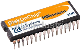
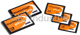
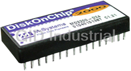

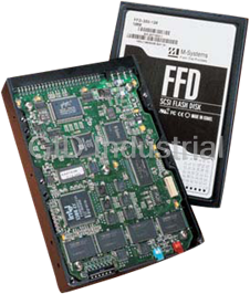
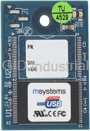


What they say about us
FANTASTIC RESOURCE
One of our top priorities is maintaining our business with precision, and we are constantly looking for affiliates that can help us achieve our goal. With the aid of GID Industrial, our obsolete product management has never been more efficient. They have been a great resource to our company, and have quickly become a go-to supplier on our list!
Bucher Emhart Glass
EXCELLENT SERVICE
With our strict fundamentals and high expectations, we were surprised when we came across GID Industrial and their competitive pricing. When we approached them with our issue, they were incredibly confident in being able to provide us with a seamless solution at the best price for us. GID Industrial quickly understood our needs and provided us with excellent service, as well as fully tested product to ensure what we received would be the right fit for our company.
Fuji
HARD TO FIND A BETTER PROVIDER
Our company provides services to aid in the manufacture of technological products, such as semiconductors and flat panel displays, and often searching for distributors of obsolete product we require can waste time and money. Finding GID Industrial proved to be a great asset to our company, with cost effective solutions and superior knowledge on all of their materials, it’d be hard to find a better provider of obsolete or hard to find products.
Applied Materials
CONSISTENTLY DELIVERS QUALITY SOLUTIONS
Over the years, the equipment used in our company becomes discontinued, but they’re still of great use to us and our customers. Once these products are no longer available through the manufacturer, finding a reliable, quick supplier is a necessity, and luckily for us, GID Industrial has provided the most trustworthy, quality solutions to our obsolete component needs.
Nidec Vamco
TERRIFIC RESOURCE
This company has been a terrific help to us (I work for Trican Well Service) in sourcing the Micron Ram Memory we needed for our Siemens computers. Great service! And great pricing! I know when the product is shipping and when it will arrive, all the way through the ordering process.
Trican Well Service
GO TO SOURCE
When I can't find an obsolete part, I first call GID and they'll come up with my parts every time. Great customer service and follow up as well. Scott emails me from time to time to touch base and see if we're having trouble finding something.....which is often with our 25 yr old equipment.
ConAgra Foods