

 Manufacturers
INTEL SE7501WV2SKU02
Description
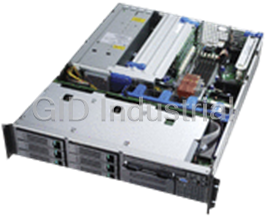
Intel SE7501WV2SKU02 Server Chassis - SR2300 SE7501WV2 BBNS SCSI CD FD FAN 500W 1+0
Part Number
SE7501WV2SKU02
Price
Request Quote
Manufacturer
INTEL
Lead Time
Request Quote
Category
Chassis & Enclosures
Specifications
Bays
6 (total) / 6 (free) x Hot-swap 3.5" x 1/3H, 1 (total) / 0 (free) x Front accessible, 1 (total) / 1 (free) x Internal 3.5" x 1H
Bundled with
Intel Server Board SE7501WV2 (SCSI)
Channel Qty
2
Chipset Type
Intel E7501
Cluster
None
Cluster Storage Controller
None
Color
Black trim
Controller Interface Type
ATA-100
Ultra320 SCSI
CPU Upgradability
Upgradable
Data Link Protocol
Fast Ethernet , Ethernet , Gigabit Ethernet
Depth
25.5 in
Device Type
Power supply
Features
Registered
Form Factor
DIMM 184-pin
Front Accessible Bays Qty
1
Front Side Bus
533 MHz
Graphics Processor / Vendor
ATI RAGE XL
Height
3 in
Hot-Swap Bays Qty
6
Installed Qty
1
Installed Size
0 MB / 12 GB (max)
Interface Type
PCI
Interfaces
1 x Storage - Ultra320 SCSI - 68 pin HD D-Sub (HD-68), Storage - ATA-100 - 40 pin IDC, 2 x USB - 4 pin USB Type A, 1 x Keyboard / mouse - Generic - 6 pin mini-DIN (PS/2 style), 2 x Network - Ethernet 10Base-T/100Base-TX/1000Base-TX - RJ-45, 1 x Display / video - VGA - 15 pin HD D-Sub (HD-15)
Internal Bays Qty
1
Max CPU Qty
2
Max Supported Qty
2
Monitor Type
none.
OS Certified
Red Hat Linux 8.0, Microsoft Windows 2000 Advanced Server, SuSE Linux Enterprise Server 8, Novell NetWare 6
Packaged Quantity
1
Power
AC 120/230 V
Power Provided
500 Watt
Power Redundancy
Optional
Power Redundancy Scheme
1+1 (with optional power supply)
Product Form Factor
Rack-mountable - 2 nm
RAID Level
RAID 1, RAID 0
Server Scalability
2-way
Slots
2 (total) / 2 (free) x Processor - Socket 604, 6 (total) / 6 (free) x Memory - DIMM 184-pin, 4 (total) / 4 (free) x PCI-X / 100 MHz, 2 (total) / 2 (free) x PCI
Software
Drivers & Utilities
Technology
DDR SDRAM - ECC
Type
1 x IDE - Integrated
1 x RAID - Integrated
CD-ROM - IDE
Integrated
loppy / CD drive combo
No CPU
None
none.
Server
Upgrade Rule
2 modules at a time
Video Memory
8 MB
Width
16.9 in
Features
- Chipset Type Intel E7501
- Rack-mountable - 2 nm Form Factor
Datasheet

Extracted Text
®
Intel Server Board
SE7501WV2
Technical Product Specification
Intel reference number C25653-001
Revision 1.0
December 2002
Enterprise Platforms and Services Division
Revision History Intel® Server Board SE7501WV2 TPS
Revision History
Date Revision Modifications
Number
11/02 0.5 First draft for internal review based on the SE7500WV2 TPS
12/02 1.0 Production Release
Disclaimers
®
Information in this document is provided in connection with Intel products. No license, express
or implied, by estoppel or otherwise, to any intellectual property rights is granted by this
document. Except as provided in Intel's Terms and Conditions of Sale for such products, Intel
assumes no liability whatsoever, and Intel disclaims any express or implied warranty, relating to
sale and/or use of Intel products including liability or warranties relating to fitness for a particular
purpose, merchantability, or infringement of any patent, copyright or other intellectual property
right. Intel products are not intended for use in medical, life saving, or life sustaining
applications. Intel may make changes to specifications and product descriptions at any time,
without notice.
Designers must not rely on the absence or characteristics of any features or instructions marked
"reserved" or "undefined." Intel reserves these for future definition and shall have no
responsibility whatsoever for conflicts or incompatibilities arising from future changes to them.
This document contains information on products in the design phase of development. Do not
finalize a design with this information. Revised information will be published when the product
is available. Verify with your local sales office that you have the latest datasheet before
finalizing a design.
®
The Intel Server Board SE7501WV2 may contain design defects or errors known as errata
which may cause the product to deviate from published specifications. Current characterized
errata are available on request.
Copyright © Intel Corporation 2003.
*Other brands and names are the property of their respective owners.
ii Revision 1.0
Intel reference number C25653-001
Intel® Server Board SE7501WV2 TPS Table of Contents
Table of Contents
1. Introduction ..........................................................................................................17
2. SE7501WV2 Server Board Overview ..................................................................18
2.1 SE7501WV2 Feature Set........................................................................... 18
3. Functional Architecture.......................................................................................21
3.1 Processor and Memory Subsystem ........................................................... 21
3.1.1 Processor Support ..................................................................................... 21
3.1.2 Memory Subsystem ................................................................................... 23
®
3.2 Intel E7501 Chipset.................................................................................. 27
3.2.1 MCH Memory Architecture......................................................................... 28
3.2.2 MCH North Bridge...................................................................................... 28
3.2.3 P64H2........................................................................................................ 29
3.2.4 ICH3-S ....................................................................................................... 30
3.3 Super I/O ................................................................................................... 32
3.3.1 GPIOs ........................................................................................................ 32
3.3.2 Serial Ports ................................................................................................ 33
3.3.3 BIOS Flash................................................................................................. 37
4. Configuration and Initialization...........................................................................38
4.1.1 Main Memory ............................................................................................. 38
4.1.2 Memory Shadowing ................................................................................... 38
4.1.3 System Management Mode Handling ........................................................ 39
4.2 I/O Map ...................................................................................................... 39
4.3 Accessing Configuration Space ................................................................. 39
4.3.1 CONFIG_ADDRESS Register ................................................................... 39
Revision 1.0 iii
Intel reference number C25653-001
Table of Contents Intel® Server Board SE7501WV2 TPS
4.4 Hardware Initialization................................................................................ 41
4.5 Clock Generation and Distribution ............................................................. 41
4.6 PCI I/O Subsystem .................................................................................... 44
4.6.1 PCI Subsystem .......................................................................................... 44
4.6.2 P32-A: 32-bit, 33-MHz PCI Subsystem...................................................... 44
4.6.3 P64-B and P64-C: 64-bit, 100-MHz PCI-X Subsystem .............................. 45
4.7 Ultra320 SCSI............................................................................................ 47
4.8 ATA-100..................................................................................................... 47
4.9 Video Controller ......................................................................................... 48
4.9.1 Video Modes.............................................................................................. 48
4.9.2 Video Memory Interface............................................................................. 49
4.9.3 Front Panel Video Memory ........................................................................ 50
4.10 Network Interface Controller (NIC)............................................................. 50
4.10.1 NIC Connector and Status LEDs ............................................................... 50
4.11 Interrupt Routing ........................................................................................ 50
4.11.1 Legacy Interrupt Routing............................................................................ 51
4.11.2 Serialized IRQ Support .............................................................................. 51
4.11.3 APIC Interrupt Routing............................................................................... 51
5. Server Management .............................................................................................54
5.1 Sahalee Baseboard Management Controller (BMC).................................. 55
5.1.1 Fault Resilient Booting ............................................................................... 61
5.2 System Reset Control ................................................................................ 62
5.2.1 Power-up Reset ......................................................................................... 62
5.2.2 Hard Reset................................................................................................. 62
5.2.3 Soft Reset .................................................................................................. 63
iv Revision 1.0
Intel reference number C25653-001
Intel® Server Board SE7501WV2 TPS Table of Contents
5.3 Intelligent Platform Management Buses (IPMB) ........................................ 63
5.4 Inter Chassis Management Bus (ICMB)..................................................... 63
5.5 Error Reporting .......................................................................................... 64
5.5.1 Error Sources and Types ........................................................................... 64
5.5.2 PCI Bus Errors........................................................................................... 64
®
5.5.3 Intel Xeon™ Processor Bus Errors .......................................................... 64
5.5.4 Memory Bus Errors .................................................................................... 64
5.5.5 Fault and Status LEDs ............................................................................... 64
5.5.6 Temperature Sensors ................................................................................ 70
6. BIOS ......................................................................................................................71
6.1 System Flash ROM Layout ........................................................................ 71
6.2 BIOS Boot Specification Compliance......................................................... 71
6.3 Memory...................................................................................................... 72
6.3.1 Memory Configuration................................................................................ 73
6.3.2 Memory Sizing and Initialization................................................................. 73
6.3.3 ECC Initialization........................................................................................ 74
6.3.4 Memory Remapping................................................................................... 74
6.3.5 DIMM Failure LED ..................................................................................... 74
6.4 Processors................................................................................................. 74
6.5 Extended System Configuration Data (ESCD), Plug and Play (PnP)......... 74
6.5.1 Resource Allocation ................................................................................... 75
6.5.2 PnP ISA Auto-Configuration....................................................................... 75
6.5.3 PCI Auto-Configuration .............................................................................. 76
6.6 NVRAM API ............................................................................................... 76
6.7 Legacy ISA Configuration .......................................................................... 76
Revision 1.0 v
Intel reference number C25653-001
Table of Contents Intel® Server Board SE7501WV2 TPS
6.8 Automatic Detection of Video Adapters ..................................................... 76
6.9 Keyboard / Mouse Configuration................................................................ 77
6.9.1 Boot without Keyboard and/or Mouse ........................................................ 77
6.10 Floppy Drives............................................................................................. 77
6.11 Universal Serial Bus (USB)........................................................................ 78
6.12 BIOS Supported Server Management Features ........................................ 78
6.12.1 IPMI ........................................................................................................... 78
6.12.2 Advanced Configuration and Power Interface (ACPI) ................................ 79
6.12.3 Wake Events.............................................................................................. 80
6.12.4 Front Panel Switches ................................................................................. 80
6.12.5 Wired For Management (WFM) ................................................................. 81
6.12.6 PXE BIOS Support..................................................................................... 82
6.12.7 BIOS Recommendations............................................................................ 82
6.13 Console Redirection................................................................................... 82
6.13.1 Operation ................................................................................................... 83
6.13.2 Keystroke Mappings .................................................................................. 83
6.13.3 Limitations.................................................................................................. 86
6.14 Emergency Management Port (EMP) ........................................................ 87
6.14.1 Serial Ports ................................................................................................ 87
6.14.2 Interaction with BIOS Console Redirection ................................................ 87
6.15 Service Partition Boot ................................................................................ 87
6.16 System Management BIOS (SMBIOS) ...................................................... 88
6.17 Microsoft* Windows* Compatibility............................................................. 90
6.17.1 Quiet Boot.................................................................................................. 91
6.18 BIOS Serviceabilty Features...................................................................... 91
vi Revision 1.0
Intel reference number C25653-001
Intel® Server Board SE7501WV2 TPS Table of Contents
6.18.1 CMOS Reset.............................................................................................. 91
6.19 BIOS Updates............................................................................................ 92
6.19.1 Flash Update Utility.................................................................................... 92
6.19.2 Loading the System BIOS.......................................................................... 93
6.19.3 User Binary Area........................................................................................ 93
6.19.4 BIOS Recovery Mode ................................................................................ 93
6.19.5 Rolling BIOS and On-line updates ............................................................. 94
6.20 BIOS and System Setup ............................................................................ 95
6.20.1 BIOS Setup Utility ...................................................................................... 95
6.20.2 Setup Utility Operation ............................................................................... 96
6.21 BIOS Security Features ........................................................................... 109
6.21.1 Operating Model ...................................................................................... 109
6.22 Password Protection ................................................................................ 110
6.23 Inactivity Timer......................................................................................... 111
6.24 Hot Key Activation.................................................................................... 111
6.25 Password Clear Jumper........................................................................... 111
6.26 Secure Mode (Unattended start).............................................................. 111
6.27 Front Panel Lock...................................................................................... 111
6.28 Video Blanking ......................................................................................... 111
6.29 PS/2 Keyboard and Mouse Lock.............................................................. 112
6.30 Secure Boot (Unattended Start)............................................................... 112
6.31 Error Handling.......................................................................................... 112
6.31.1 Error Sources and Types ......................................................................... 112
6.32 SMI Handler............................................................................................. 113
6.33 PCI Bus Error........................................................................................... 113
Revision 1.0 vii
Intel reference number C25653-001
Table of Contents Intel® Server Board SE7501WV2 TPS
6.34 Processor Bus Error................................................................................. 113
6.35 Single-Bit ECC Error Throttling Prevention .............................................. 113
6.36 System Limit Error ................................................................................... 114
6.37 Boot Event ............................................................................................... 114
6.38 Fault Resilient Booting (FRB)................................................................... 114
6.38.1 FRB3........................................................................................................ 114
6.38.2 FRB2........................................................................................................ 114
6.39 Boot Monitoring........................................................................................ 116
6.39.1 Purpose.................................................................................................... 116
6.40 Logging Format Conventions................................................................... 118
6.40.1 Memory Error Events ............................................................................... 118
6.40.2 PCI Error Events...................................................................................... 120
6.40.3 FRB-2 Error Events.................................................................................. 121
6.41 POST Codes, Error Messages, and Error Codes .................................... 122
6.41.1 POST Progress Code LEDs..................................................................... 122
6.41.2 POST Error Codes and Messages........................................................... 123
6.41.3 POST Error Beep Codes.......................................................................... 125
6.41.4 BIOS Recovery Beep Codes.................................................................... 125
6.41.5 Bootblock Error Beep Codes.................................................................... 126
6.42 "POST Error Pause" Option..................................................................... 127
6.43 SE7501WV2 Server Board BIOS Runtime APIs...................................... 127
6.44 INT 15 Extensions.................................................................................... 127
6.44.1 Cache Services........................................................................................ 127
6.44.2 Intel ID String ........................................................................................... 128
6.44.3 Processor Information.............................................................................. 129
viii Revision 1.0
Intel reference number C25653-001
Intel® Server Board SE7501WV2 TPS Table of Contents
6.44.4 Extended NVRAM Services ..................................................................... 129
6.44.5 IPMB Services ......................................................................................... 130
6.44.6 INT15h, Function DA20h, Subfunction 99h/9Ah/9Bh – Read/Write/Bus
Master Write IMB .................................................................................................. 130
6.45 Multiple Processor Support (MPS)........................................................... 130
6.45.1 Multiprocessor Specification Support....................................................... 130
6.45.2 Multiple Processor Support...................................................................... 131
6.45.3 Mixed Processor Support......................................................................... 131
6.46 Hyper-Threading Technology................................................................... 132
6.47 OEM Customization ................................................................................. 132
6.48 User Binary .............................................................................................. 132
6.48.1 Scan Point Definitions.............................................................................. 134
6.48.2 Format of the User Binary Information Structure...................................... 135
6.48.3 OEM Splash Screen ................................................................................ 135
6.48.4 Localization.............................................................................................. 135
7. SE7501WV2 ACPI Implementation....................................................................136
7.1 ACPI ........................................................................................................ 136
7.1.1 Front Panel Switches ............................................................................... 136
7.1.2 Wake up Sources (ACPI and Legacy) ..................................................... 138
8. SE7501WV2 Connectors....................................................................................139
8.1 Power Connectors ................................................................................... 139
8.2 Memory Module Connector...................................................................... 140
8.3 Processor Socket..................................................................................... 141
8.4 System Management Headers................................................................. 143
8.4.1 ICMB Header ........................................................................................... 143
8.4.2 OEM IPMB Header .................................................................................. 143
Revision 1.0 ix
Intel reference number C25653-001
Table of Contents Intel® Server Board SE7501WV2 TPS
8.5 PCI I/O Riser Slot Connector ................................................................... 143
8.6 Front Panel Connectors ........................................................................... 146
8.6.1 High Density 100-Pin Floppy / Front Panel / IDE Connector (J2G1)........ 148
8.6.2 VGA Connector........................................................................................ 150
8.6.3 SCSI Connectors ..................................................................................... 150
8.6.4 NIC Connector ......................................................................................... 151
8.6.5 ATA RAID Connectors ............................................................................. 152
8.6.6 USB Connector ........................................................................................ 153
8.6.7 Floppy Connector..................................................................................... 154
8.6.8 Serial Port Connector............................................................................... 155
8.6.9 Keyboard and Mouse Connector ............................................................. 155
8.7 Miscellaneous Headers............................................................................ 156
8.7.1 Fan Headers ............................................................................................ 156
9. Configuration Jumpers......................................................................................157
9.1 System Recovery and Update Jumpers................................................... 157
9.2 External RJ45 Serial Port Jumper Block .................................................. 158
10. General Specifications.......................................................................................159
10.1 Absolute Maximum Ratings ..................................................................... 159
10.2 Power Information.................................................................................... 159
10.2.1 SE7501WV2 Server Board Power Budget............................................... 159
10.3 Power Supply Specifications.................................................................... 160
10.3.1 Power Timing........................................................................................... 160
10.3.2 Voltage Recovery Timing Specifications.................................................. 163
11. Regulatory and Integration Information...........................................................164
11.1 Product Regulatory Compliance .............................................................. 164
x Revision 1.0
Intel reference number C25653-001
Intel® Server Board SE7501WV2 TPS Table of Contents
11.1.1 Product Safety Compliance...................................................................... 164
11.1.2 Product EMC Compliance........................................................................ 164
11.1.3 Product Regulatory Compliance Markings............................................... 164
11.2 Electromagnetic Compatibility Notices..................................................... 165
11.2.1 Europe (CE Declaration of Conformity).................................................... 165
11.2.2 Australian Communications Authority (ACA) (C-Tick Declaration of
Conformity)............................................................................................................ 165
11.2.3 Ministry of Economic Development (New Zealand) Declaration of
Conformity............................................................................................................. 165
11.2.4 BSMI (Taiwan) ......................................................................................... 165
11.3 Replacing the Back up Battery................................................................. 165
12. Mechanical Specifications.................................................................................167
12.1 PCI Riser Cards....................................................................................... 168
12.1.1 1-Slot 3.3V PCI Riser Card ...................................................................... 168
12.1.2 3-Slot 3.3V PCI Riser Card ...................................................................... 168
Appendix A: Glossary.............................................................................................169
Revision 1.0 xi
Intel reference number C25653-001
List of Figures Intel® Server Board SE7501WV2 TPS
List of Figures
®
Figure 1. Intel Server Board SE7501WV2 Block Diagram........................................... 20
Figure 2. Memory Sub-system Block Diagram ............................................................. 24
Figure 3. Memory Bank Label Definition ...................................................................... 26
Figure 4. Serial Port Mux Logic ..................................................................................... 35
Figure 5. J5A2 Jumper Block for DCD Signal ............................................................... 36
Figure 6. J5A2 Jumper Block for DSR Signal................................................................ 36
Figure 7. CONFIG_ADDRES Register.......................................................................... 40
®
Figure 8. Intel Server Board SE7501WV2 Clock Distribution ...................................... 43
®
Figure 9. Intel Server Board SE7501WV2 Sahalee BMC Block Diagram.................... 54
Figure 10. BIOS Boot Monitoring Flowchart ................................................................ 117
®
Figure 11. Intel Server Board SE7501WV2 Configuration Jumpers (J1D4) .............. 157
Figure 12. Output Voltage Timing ............................................................................... 161
Figure 13. Turn On / Off Timing .................................................................................. 162
®
Figure 14. Intel Server Board SE7501WV2 Mechanical Drawing.............................. 167
Figure 15. 1-Slot PCI Riser Mechanical Drawing ........................................................ 168
Figure 16. 3-Slot PCI Riser Mechanical Drawing ........................................................ 168
xii Revision 1.0
Intel reference number C25653-001
Intel® Server Board SE7501WV2 TPS List of Tables
List of Tables
®
Table 1. Intel Server Board SE7501WV2 Processor Support Matrix for 533MHz ....... 21
®
Table 2. Intel Server Board SE7501WV2 Processor Support Matrix for 400MHz ....... 22
Table 3. Memory Bank Labels....................................................................................... 25
Table 4. P64-B Speeds ................................................................................................. 29
Table 5. P64-C Speeds................................................................................................. 30
Table 6. Super I/O GPIO Usage Table.......................................................................... 32
Table 7. Serial A Header Pin-out................................................................................... 34
Table 8. Rear Serial Port B Adapter Pinout................................................................... 36
Table 9. PCIdevice IDs.................................................................................................. 40
Table 10. PCI Bus Segment Characteristics ................................................................. 44
Table 11. P32-A Configuration IDs................................................................................ 44
Table 12. P32-Arbitration Connections.......................................................................... 45
Table 13. P64-B Configuration IDs................................................................................ 45
Table 14. P64-C Configuration IDsIDs .......................................................................... 45
Table 15. P64-B Arbitration Connections ...................................................................... 46
Table 16. P64-C Arbitration Connections ...................................................................... 46
Table 17. Video Modes ................................................................................................ 49
Table 18. Video Memory Interface ................................................................................ 49
Table 19. Interrupt Definitions ....................................................................................... 51
®
Table 20. Intel Server Board SE7501WV2 Interrupt Mapping ..................................... 52
Table 21. BMC Pinout ................................................................................................... 55
Table 22. ADM1026 Input Definition.............................................................................. 60
®
Table 23. Intel Server Board SE7501WV2 I2C Address Map...................................... 63
Table 24. System Status LEDs ..................................................................................... 65
Table 25. Boot Block POST Progress Codes................................................................ 67
Table 26. Allowed Combinations of Floppy Drive and Floppy Media............................. 77
Table 27. Supported Wake Events................................................................................ 80
Table 28. Non-ASCII Key Mappings............................................................................. 84
Table 29. ASCII Key Mappings ..................................................................................... 86
Table 30. SMBIOS Header Structure ............................................................................ 89
Revision 1.0 xiii
Intel reference number C25653-001
List of Tables Intel® Server Board SE7501WV2 TPS
Table 31. Setup Utility Screen....................................................................................... 97
Table 32. Keyboard Command Bar............................................................................... 97
Table 33. Main Menu Selections ................................................................................... 99
Table 34. Primary Master and Slave Adapters Sub-menu Selections......................... 100
Table 35. Processor Settings Sub-menu..................................................................... 100
Table 36. Advanced Menu Selections......................................................................... 101
Table 37. Advanced Chipset Control Sub-menu Selections........................................ 101
Table 38. PCI Configuration Sub-menu Selections .................................................... 101
Table 39. PCI Device, Embedded Devices ................................................................. 102
Table 40. I/O Device/Peripheral Configuration Sub-menu Selections ........................ 102
Table 41. Memory Configuration Menu Selections...................................................... 103
Table 42. Security Menu Selections............................................................................ 103
Table 43. Server Menu Selections .............................................................................. 104
Table 44. System Management Sub-menu Selections................................................ 105
Table 45. Serial Console Redirection Sub-menu Selections ....................................... 106
Table 46. Event Log Configuration Sub-menu Selections ........................................... 106
Table 47. Fault Resilient Boot Sub-menu Selections .................................................. 107
Table 48. Boot Menu Selections ................................................................................. 107
Table 49. Boot Device Priority Selections .................................................................. 107
Table 50. Hard Drive Selections.................................................................................. 108
Table 51. Removable Devices Selections ................................................................... 108
Table 52. Exit Menu Selections................................................................................... 108
Table 53. Security Features Operating Model............................................................. 109
Table 54. Memory Error Event Data Field Contents.................................................... 119
Table 55. PCI Error Event Data Field Contents........................................................... 120
Table 56. Examples of Event Data Field Contents for PCI Errors ............................... 121
Table 57. FRB-2 Event Data Field Contents ............................................................... 121
Table 58. Examples of Event Data Field Contents for FRB-2 Errors.......................... 122
Table 59. POST Progress Code LED Example........................................................... 123
Table 60. Standard POST Error Messages and Codes............................................... 123
Table 61. Extended POST Error Messages and Codes.............................................. 124
Table 62. BIOS Recovery Beep Codes....................................................................... 125
Table 63. Bootblock Error Beep Codes....................................................................... 126
xiv Revision 1.0
Intel reference number C25653-001
Intel® Server Board SE7501WV2 TPS List of Tables
Table 64. Three-beep Boot Block Memory Failure Error Codes.................................. 126
Table 65. Interrupt 15h Extensions.............................................................................. 127
Table 66. User Binary Area Scan Point Definitions ..................................................... 134
Table 67. User Binary Information Structure ............................................................... 135
Table 68. Supported Wake Events.............................................................................. 138
Table 69. Power Connector Pin-out (J3J1) ................................................................. 139
Table 70. Power Supply Signal Connector (J1J1)....................................................... 139
Table 71. 12V Power Connector (J4J1) ...................................................................... 139
Table 72. DIMM Connectors (J5F1, J5F2, J5F3, J6F1, J6F2, J6F3) .......................... 140
Table 73. Socket 604 Processor Socket Pinout .......................................................... 141
Table 74. ICMB Header Pin-out (J9B2)....................................................................... 143
Table 75. IPMB Header Pin-out (J9C1)....................................................................... 143
Table 76. P64-B Full Length PCI Riser Slot Pin-out.................................................... 143
Table 77. P64-C Low-Profile Riser Slot Pin-out .......................................................... 144
Table 78. 34-pin Front Panel Connector Signal Descriptions...................................... 146
Table 79. SSI Compliant 24-pin Front Panel Connector Pinout (J1H1)...................... 148
Table 80. High density 100-Pin Floppy/Front Panel/IDE Connector Pin out (J2G1).... 148
Table 81. VGA Connector Pin-out (J8A1) ................................................................... 150
Table 82. 68-pin VHDCI SCSI and Wide Connectors Pin-out (J7B1, J7A1)................ 150
Table 83. Stacked Dual RJ-45 Connector Pin-out (JA6A1)......................................... 151
Table 84. ATA-100 RAID 40-pin Connectors Pin-out (J1D1, J1D2) ............................ 152
Table 85. ATA-100 Legacy 40-pin Connector Pinout (J1G2) ...................................... 153
Table 86. USB Connectors Pin-out (J4A1, J9A1)........................................................ 153
Table 87. Optional USB Connection Header Pin-out (J1D3)...................................... 154
Table 88. Legacy 34-pin Floppy Connector Pin-out (J1G1) ........................................ 154
Table 89. Rear Low-Profile RJ-45 Serial B Port Pin-out (J5A1) .................................. 155
Table 90. 9-pin Header Serial A Port Pin-out (J9A2)................................................... 155
Table 91. Keyboard and Mouse PS/2 Connector Pin-out (J6A1) ................................ 156
Table 92. Three-pin Fan Headers Pin-out (J4J2, J7J1)............................................... 156
Table 93. Fan Pack Fan Header Pin-out (J3J2) .......................................................... 156
Table 94. Configuration Jumper Options..................................................................... 157
Table 95. Absolute Maximum Ratings......................................................................... 159
®
Table 96. Intel Server Board SE7501WV2/SR2300/SR1300 Power Budget ............. 159
Revision 1.0 xv
Intel reference number C25653-001
List of Tables Intel® Server Board SE7501WV2 TPS
®
Table 97. Intel Server Board SE7501WV2 Static Power Supply Voltage Specification160
®
Table 98. Intel Server Board SE7501WV2 Dynamic Power Supply Voltage
Specification.......................................................................................................... 160
Table 99. Voltage Timing Parameters......................................................................... 161
Table 100. Turn On / Off Timing.................................................................................. 161
xvi Revision 1.0
Intel reference number C25653-001
Intel® Server Board SE7501WV2 TPS Introduction
1. Introduction
®
The Intel SE7501WV2 server board Technical Product Specification (TPS) provides a high-
®
level technical description for the Intel SE7501WV2 server board. It details the architecture and
feature set for all functional sub-systems that make up the server board.
This document is sub-divided into the following main categories:
Chapter 2: SE7501WV2 Server Board Overview
Chapter 3: Functional Architecture
Chapter 4: Configuration and Initialization
Chapter 5: Server Management
Chapter 6: BIOS
Chapter 7: SE7501WV2 Server Board ACPI Implementation
Chapter 8: SE7501WV2 Server Board Connectors
Chapter 9: Configuration Jumpers
Chapter 10: General Specifications
Chapter 11: Regulatory and Integration Information
Chapter 12: Mechanical Specification
The contents of this document are derived from several of the SE7501WV2’s External Product
Specifications (EPS). For a more detailed, lower level description of a particular functional sub-
system, the EPS for the sub-system should be ordered from your Intel field representative. The
EPS documents available for the SE7501WV2 server board include the following:
®
• Intel SE7501WV2 server board BIOS EPS
®
• Intel SE7501WV2 server board Baseboard Management Controller EPS
• Sahalee Core BMC EPS for IPMI v1.5 System
The SE7501WV2 server board supports the Intel® Server Management Version 5.5 software.
One additional EPS document is available to provide technical detail on the feature set of the
server management software. This document is:
• ISM Customization EPS
Revision 1.0 17
Intel reference number C25653-001
SE7501WV2 Server Board Overview Intel® Server Board SE7501WV2
2. SE7501WV2 Server Board Overview
The SE7501WV2 server board is a monolithic printed circuit board with features that were
designed to support the high-density 1U and 2U server market.
2.1 SE7501WV2 Feature Set
Two different SE7501WV2 server boards will be made available. One will provide an embedded
Ultra-320* SCSI interface and the other will provide an embedded ATA-100* “Value-Raid”
interface. Both boards support the following feature set:
®
• Dual Intel Xeon™ processor in the Socket 604 INT3/FCPGA package
• 533 MHz Front Side Bus
®
• Intel E7501 chipset
- E7501 North Bridge
- P64H2 I/O Bridge
- ICH3-S South Bridge
• Support for up to six DDR266 compliant registered ECC DIMMs providing up to 12 GB of
memory, when 2G DIMMs become available and have been tested. (Will support
DDR200 modules when 400MHz processors are installed.)
• Three separate and independent PCI buses:
- Segment A: 32-bit, 33 MHz, 5 V (P32-A) with two embedded devices:
• 2D/3D graphics controller: ATI Rage* XL Video Controller with 8 MB of
memory
• ATA-100 controller: Promise Technology* PDC20277 (ATA-100 board only)
- Segment B: 64-bit, 133 MHz, 3.3 V, PCI-X (P64-B) supporting the following
configuration:
• One PCI I/O riser slot capable of supporting full length PCI add-in cards
• Dual-channel Intel® 10/100/1000 82546EB Gigabit Ethernet Controller
- Segment C: 64-bit, 133 MHz, 3.3 V PCI-X (P64-C) supporting the following
devices:
• One PCI I/O riser slot capable of supporting low-profile PCI add-in cards
• Dual-channel SCSI with Zero Channel RAID (ZCR) and host RAID support
(SCSI SKU only)
• LPC (Low Pin Count) bus segment with two embedded devices:
- Platform Management Controller (PMC) providing monitoring, alerting, and
logging of critical system information obtained from embedded sensors on the
server board
- Super I/O controller chip providing all PC-compatible I/O (floppy, serial,
keyboard, mouse)
• X-Bus segment with one embedded device:
18 Revision 1.0
Intel reference number C25653-001
Intel® Server Board SE7501WV2 TPS SE7501WV2 Server Board Overview
®
- Flash ROM device for system BIOS: Intel 32-megabit 28F320C3 Flash ROM
• Two external Universal Serial Bus (USB) ports with an additional internal header
providing two optional USB ports for front panel support
• One external low-profile RJ45 serial port. An internal header is also available providing
an optional serial port.
• One IDE connector, supporting one or two ATA-100 compatible devices
• Support for up to seven system fans
• Fault/Status LEDs throughout the server board
• Multiple server management headers providing on-board interconnects to server
management features
• SSI-compliant connectors for SSI interface support: front panel, floppy, and ATA-33
Figure 1 shows the functional blocks of the server board and the plug-in modules that it
supports.
Revision 1.0 19
Intel reference number C25653-001
SE7501WV2 Server Board Overview Intel® Server Board SE7501WV2
®
Figure 1. Intel Server Board SE7501WV2 Block Diagram
20 Revision 1.0
Intel reference number C25653-001
Intel® Server Board SE7501WV2 TPS Functional Architecture
3. Functional Architecture
This chapter provides a high-level description of the functionality distributed between the
architectural blocks of the SE7501WV2 server board.
3.1 Processor and Memory Subsystem
The E7501 chipset provides a 36-bit address, 64-bit data processor host bus interface,
operating at 400MHz and 533Mz in the AGTL+ signaling environment. The MCH component of
the chipset provides an integrated memory controller, an 8-bit Hub Interface, and three 16-bit
Hub Interfaces.
The Hub Interface provides the interface to two 64-bit, 133-MHz, Rev 1.0 compliant PCI-X
buses via the P64H2. The SE7501WV2 server board directly supports up to 12 GB of ECC
memory, using six DDR266 compliant registered ECC DIMMs. (Will support DDR200 modules
when 400MHz processors are installed.) The ECC implementation in the MCH can detect and
correct single-bit errors, detect multiple-bit errors, and support the Intel® Single Device Data
Correction features.
3.1.1 Processor Support
®
The SE7501WV2 server board supports one or two Intel Xeon™ processors in the Socket 604
INT3/FCPGA package. When two processors are installed, all processors must be of identical
revision, core voltage, and bus/core speed. When only one processor is installed, it should be in
the socket labeled CPU-1 and the other socket must be empty. The support circuitry on the
server board consists of the following:
• Dual Socket 604 INT3/FCPGA CPU sockets supporting 533 MHz (will support 400 MHz
processors running at 400 Mhz speed.)
• Processor host bus AGTL+ support circuitry
®
Table 1. Intel Server Board SE7501WV2 Processor Support Matrix for 533MHz
Test L2
Speed (MHz)
Product Code MM# Specification Stepping CPUID Cache Notes
533MHz
(S-spec) Size
2.8 GHz (1U) BX80532KE2800DU 851292 SL6GG C1 0F24 512k 1
2.8 GHz (1U) BX80532KE2800DU 851275 SL6NS C1 0F24 512k 1
2.8 GHz BX80532KE2800D 851275 SL6NS C1 0F24 512k 1
2.8gGHz BX80532KE2800D 851285 SL6GG C1 0F24 512k 1
2.66 GHz (1U) BX80532KE2667DU 851650 SL6GF C1 0F24 512k 1
2.66 GHz (1U) BX80532KE2667DU 851713 SL6NR C1 0F24 512k 1
2.66 GHz BX80532KE2667D 851647 SL6GF C1 0F24 512k 1
2.66 GHz BX80532KE2667D 851712 SL6GF C1 0F24 512k 1
2.4 GHz (1U) BX80532KE2400DU 851290 SL6GD C1 0F24 512k 1
2.4 GHz (1U) BX80532KE2400DU 851273 SL6NQ C1 0F24 512k 1
2.4 GHz BX80532KE2400D 851280 SL6GD C1 0F24 512k 1
2.4 GHz BX80532KE2400D 851269 SL6NQ C1 0F24 512k 1
2.0 GHz (1U) BX80532KE2000DU 851288 SL6RQ C1 0F24 512k 1
2.0 GHz (1U) BX80532KE2000DU 851272 SL6NP C1 0F24 512k 1
2.0 GHz BX80532KE2000D 851279 SL6NP C1 0F24 512k 1
2.0 GHz BX80532KE2000D 851268 SL6NP C1 0F24 512k 1
Revision 1.0 21
Intel reference number C25653-001
Functional Architecture Intel® Server Board SE7501WV2
®
Table 2. Intel Server Board SE7501WV2 Processor Support Matrix for 400MHz
Test L2
Speed (MHz)
Product Code MM# Specification Stepping CPUID Cache Notes
400MHz
(S-spec) Size
2.8 GHz BX80532KC2800D 850007 SL6MS C1 0F24 512k 1
2.8 GHz 80532KC072512 849546 SL6M7 C1 0F24 512k 1
2.8GHz (1U) BX80532KC2800DU 850614 SL6M7 C1 0F24 512k 1
2.6 GHz BX80532KC2600D 850609 SL6EQ C1 0F24 512k 1
2.6 GHz 80532KC064512 847694 SL6EQ C1 0F24 512k 1
2.6 GHz (1U) BX80532KC2600DU 849701 SL6EQ C1 0F24 512k 1
2.4 GHz BX80532KC2400D 845163 SL687 tB0 0F24 512k 1
2.4 GHz 80532KC056512 847695 SL6EP C1 0F24 512k 1
2.4 GHz BX80532KC2400D 851738 SL6EP C1 0F24 512k 1
2.4 GHz (1U) BX80532KC2400DU 849703 SL6K2 B0 0F24 512k 1
2.2 GHz BX80532KC2200D 843623 SL624 tB0 0F24 512k 1
2.2 GHz 80532KC049512 849112 SL6JZ C1 0F24 512k 1
2.2 GHz BX80532KC2200D 49356 SL6JZ C1 0F24 512k 1
2.2 GHz (1U) BX80532KC2200DU 848431 SL624 tB0 0F24 512k 1
2.0 GHz BX80532KC2000D 843637 SL623 tB0 0F24 512k 1
2.0 GHz 80532KC041512 849063 SL6JY C1 0F24 512k 1
1.8 GHz BX80532KC1800D 843620 SL622 tB0 0F24 512k 1
1.8 GHz 80532KC033512 849064 SL6JX C1 0F24 512k 1
1.8 GHz (1U) BX80532KC1800DU 848419 SL622 tB0 0F24 512k 1
Notes: Processors must be populated in sequential order. That is, CPU socket #1 must be
populated before CPU socket #2.
• The SE7501WV2 server board is designed to provide up to 75 A per processor.
Processors with higher current requirements are not supported.
• Processor terminators are not required in unpopulated processor sockets.
In addition to the circuitry described above, the processor subsystem contains the following:
• Processor module presence detection logic
• Server management registers and sensors
3.1.1.1 Processor VRM
The SE7501WV2 baseboard has a single VRM (Voltage Regulator Module) to support two
processors. It is compliant with the VRM 9.1 specification and provides a maximum of 150
AMPs, which is capable of supporting currenlyt supported processors as well as those
supported in the future.
The board hardware and BMC must read the processor VID (voltage identification) bits for each
processor before turning on the VRM. If the VIDs of the two processors are not identical, then
the BMC will not turn on the VRM and a beep code is generated.
22 Revision 1.0
Intel reference number C25653-001
Intel® Server Board SE7501WV2 TPS Functional Architecture
3.1.1.2 Reset Configuration Logic
The BIOS determines the processor stepping, cache size, etc through the CPUID instruction.
The requirements are that all processors in the system must operate at the same frequency,
have the same cache sizes, and have the same VID. No mixing of product families is supported.
On the SE7501WV2 platform, the BIOS is responsible for configuring the processor speeds.
The processor information is read at every system power-on. The speed is set to correspond to
the speed of the slowest processor installed.
Note: No manual processor speed setting options exist either in the form of a BIOS setup option
or jumpers when using production level processors.
3.1.1.3 Processor Module Presence Detection
Logic is provided on the baseboard to detect the presence and identity of installed processors.
The BMC checks the logic and will not turn on the system DC power unless the VIDs of both
processors match in a dual processor configuration.
3.1.1.4 Interrupts and APIC
Interrupt generation and notification to the processors is done by the APICs in the ICH3 and the
P64H2 using messages on the front side bus.
3.1.1.5 Server Management Registers and Sensors
The Baseboard Management Controller manages registers and sensors associated with the
processor / memory subsystem. For more information, refer to Section 5.
3.1.2 Memory Subsystem
The SE7501WV2 server board supports up to six DIMM slots for a maximum memory capacity
of 12 GB. The DIMM organization is x72, which includes eight ECC check bits. The memory
interface runs at 266MHz. (200MHz when DDR200 DRAM’s and 400MHz processors are used.)
The memory controller supports memory scrubbing, single-bit error correction, multiple-bit error
detection, and the Intel® Single Device Data Correction feature. Memory can be implemented
with either single sided (one row) or double-sided (two row) DIMMs.
The following figure provides a block diagram of the memory sub-system implemented on the
SE7501WV2 server board.
Revision 1.0 23
Intel reference number C25653-001
Functional Architecture Intel® Server Board SE7501WV2
Figure 2. Memory Sub-system Block Diagram
3.1.2.1 Memory DIMM Support
The SE7501WV2 server board supports DDR266 compliant registered ECC DIMMs operating at
266MHz. (DDR200 DIMMs are supported when 400MHz processors are used.)
Only DIMMs tested and qualified by Intel or a designated memory test vendor are supported on
the SE7501WV2 server board. A list of tested DIMMs will be made available. Note that all
DIMMs are supported by design, but only fully tested DIMMs will be supported.
The minimum supported DIMM size is 128 MB. Therefore, the minimum main memory
configuration is 2 x 128 MB or 256 MB. The largest size DIMM supported is a 2 GB stacked
registered DDR266 ECC DIMM based on 512 megabit technology. (DDR200 DIMMs are
supported when 400MHz processors are used)
Only registered DDR266 compliant, ECC, DDR memory DIMMs will be supported. (DDR200
DIMMs are supported when 400MHz processors are used.)
• ECC single-bit errors will be corrected and multiple-bit errors will be detected. The
SE7501WV2 server board also supports the Intel® Single Device Data Correction
feature.
• The maximum memory capacity is 12 GB.
• The minimum memory capacity is 256 MB.
3.1.2.2 Memory Configuration
The memory interface between the MCH and DIMMs is 144 bits wide. This requires that two
DIMMs be populated per bank in order for the system to operate. At least one bank has to be
24 Revision 1.0
Intel reference number C25653-001
Intel® Server Board SE7501WV2 TPS Functional Architecture
populated in order for the system to boot. If additional banks have less than two DIMMs, the
memory for that bank(s) will not be available to the system.
There are three banks of DIMMs, labeled 1, 2, and 3. Bank 1 contains DIMM locations 1A and
1B, Bank 2 contains 2A and 2B, and Bank 3 contains 3A and 3B. DIMM socket identifiers are
marked with silkscreen next to each DIMM socket on the baseboard. Note that the sockets
associated with any given bank are located next to each other.
Certain combinations of DIMM types in the same system can violate the write Ringback
measurement specification during analog validation.
• When mixing double-ranked DIMMs (x4 or x8) with single-ranked DIMMs (x4 or x8), if a
single-ranked DIMM is placed in the populated slot closest to the MCH, the Write Ringback
at that DIMM violates the JEDEC DRAM specification.
The baseboard’s signal integrity and cooling are optimized when memory banks are populated
in order. Therefore, when installing memory, DIMMs should be installed starting with Bank 1 and
ending with Bank 3.
DIMM and memory configurations must adhere to the following:
• DDR266 registered ECC DIMM modules (DDR200 when 400MHz processors are used)
• DIMM organization: x72 ECC
• Pin count: 184
• DIMM capacity: 128 MB, 256 MB, 512 MB, 1 GB, 2 GB
• Serial PD: JEDEC Rev 2.0
• Voltage options: 2.5 V (VDD/VDDQ)
• Interface: SSTL2
• Two DIMMs must be populated in a bank for a x144 wide memory data path.
• Any or all memory banks may be populated.
Table 3. Memory Bank Labels
Memory DIMM Bank
J5F1 (DIMM 1B), J5F2 (DIMM 1A) 1
J5F3 (DIMM 2B), J6F1 (DIMM 2A) 2
J6F2 (DIMM 3B), J6F3 (DIMM 3A) 3
Revision 1.0 25
Intel reference number C25653-001
Functional Architecture Intel® Server Board SE7501WV2
J5F1 J5F2 J5F3 J6F1 J6F2 J6F3
1B 1A 2B 2A 3B 3A
Bank 1 Bank 3
Bank 2
Figure 3. Memory Bank Label Definition
2
3.1.2.3 I C*Bus
2
An I C* bus connects the six DIMM slots to the ICH3-S and the BMC. This bus is used by the
system BIOS to retrieve DIMM information needed to program the MCH memory registers which
are required to boot the system.
3.1.2.4 DIMM Failure LED
The SE7501WV2 server board provides DIMM Failure LEDs located next to each DIMM slot on
the baseboard. The DIMM Failure LEDs are used to indicate double-bit DIMM errors. If a
26 Revision 1.0
Intel reference number C25653-001
Intel® Server Board SE7501WV2 TPS Functional Architecture
double-bit error is detected during POST, the BIOS sends a Set DIMM State command to the
BMC indicating that the DIMM LED is lit.
3.1.2.5 Intel® Single Device Data Correction feature
The SE7501WV2 server board supports Intel’s Single Device Data Correction correct memory
architecture, which gives the memory sub-system the ability to withstand a multi-bit failure within
a DRAM device, including a failure that causes incorrect data on all data bits of the device.
®
3.2 Intel E7501 Chipset
®
The SE7501WV2 server board is designed around the Intel E7501 chipset. The chipset
provides an integrated I/O bridge and memory controller, and a flexible I/O subsystem core
(PCI-X). This is targeted for multiprocessor systems and standard high-volume servers. The
Intel E7501 chipset consists of three components:
• MCH: Memory Controller Hub North Bridge. The MCH North Bridge accepts access
requests from the host (processor) bus and directs those accesses to memory or to one
of the PCI buses. The MCH monitors the host bus, examining addresses for each
request. Accesses may be directed to a memory request queue for subsequent
forwarding to the memory subsystem, or to an outbound request queue for subsequent
forwarding to one of the PCI buses. The MCH also accepts inbound requests from the
P64H2 and the ICH3-S. The MCH is responsible for generating the appropriate controls
to control data transfer to and from memory.
• P64H2: PCI-X 64bit Hub 2.0 I/O Bridge. The P64H2 provides the interface for two 64-
bit, 133MHz Rev. 1.0 compliant PCI-X buses. The P64H2 is both master and target on
both PCI-X buses.
• ICH3-S: South Bridge. The ICH3-S controller has several components. It provides the
interface for a 32-bit, 33-MHz Rev. 2.2-compliant PCI bus. The ICH3-S can be both a
master and a target on that PCI bus. The ICH3-S also includes a USB controller and an
IDE controller. The ICH3-S is also responsible for much of the power management
functions, with ACPI control registers built in. The ICH3-S also provides a number of
GPIO pins and has the LPC bus to support low speed legacy I/O.
The MCH, P64H2, and ICH3-S chips provide the pathway between processor and I/O systems.
The MCH is responsible for accepting access requests from the host (processor) bus, and
directing all I/O accesses to one of the PCI buses or legacy I/O locations. If the cycle is directed
to one of the 64-bit PCI segments, the MCH communicates with the P64H2 through a private
interface called the HI (Hub Interface). If the cycle is directed to the ICH3-S, the cycle is output
on the MCH’s 8bit HI 1.5 bus. The P64H2 translates the HI 2.0 bus operation to a 64-bit PCI-X
Rev. 1.0-compliant signaling environment operating from 100MHz to 133 MHz. The ICH3-S
translates the HI 1.5 bus operation to a 32-bit PCI Rev. 2.2-compliant signaling environment
operating at 33MHz.
The HI 2.0 bus is 16 bits wide and operates at 66 MHz with 512MT/s, providing over 1 GB per
second of bandwidth.
All I/O for the SE7501WV2 server board, including PCI and PC-compatible I/O, is directed
through the MCH and then through either the P64H2 or the ICH3-S provided PCI buses.
Revision 1.0 27
Intel reference number C25653-001
Functional Architecture Intel® Server Board SE7501WV2
• The ICH3-S provides a 32-bit/33-MHz PCI bus hereafter called P32-A.
• The P64H2 provides two independent 64-bit, 133-MHz PCI-X buses hereafter called
P64-B, and P64-C.
This independent bus structure allows all three PCI buses to operate concurrently.
3.2.1 MCH Memory Architecture
The MCH supports a 144-bit wide Memory Sub-system that can support a maximum of 12 GB
(using 2 GB DIMMs). This configuration needs external registers for buffering the memory
address and control signals. In this configuration the MCH supports six DDR266 compliant
registered stacked DIMMs for a maximum of 12 GB. (DDR200 DIMMs are supported when
400MHz processors are used.) The six chip selects are registered inside the MCH and need no
external registers for chip selects.
The memory interface runs at 266 MHz. (200 MHz when DDR-200 modules and 400 MHz
processors are used.) The memory interface supports a 144-bit wide memory array. It uses
fifteen address lines (BA[1:0] and MA[12:0]) and supports 64 Mb, 128 Mb, 256 Mb, 512 Mb
DRAM densities. The DDR DIMM interface supports memory scrubbing, single-bit error
correction, and multiple bit error detection as well as the Intel® Single Device Data Correction
features.
3.2.1.1 DDR Configurations
The DDR interface supports up to 12GB of main memory and supports single- and double-density
DIMMs.
3.2.2 MCH North Bridge
The E7501 MCH North Bridge (MCH) is a 1005 ball FC-BGA device and uses the proven
® ®
components of previous generations like the Intel Pentium 4 bus interface unit, the Hub
Interface unit, and the DDR memory interface unit. In addition, the MCH incorporates a Hub
Interface (HI). The hub interface enables the MCH to directly interface with the P64H2. The
MCH also increases the main memory interface bandwidth and maximum memory configuration
with a 144-bit wide memory interface.
The MCH integrates three main functions:
• An integrated high performance main memory subsystem.
• An HI 2.0 bus interface that provides a high-performance data flow path between the
host bus and the I/O subsystem.
• A HI 1.5 bus which provides an interface to the ICH3-S (South Bridge).
Other features provided by the MCH include the following:
• Full support of ECC on the memory bus
• Full support of the Intel® Single Device Data Correction features.
• Twelve deep in-order queue
• Full support of registered DDR266 ECC DIMMs (DDR200 DIMMs when 400MHz
processors are used)
• Support for 12 GB of DDR memory
• Memory scrubbing
28 Revision 1.0
Intel reference number C25653-001
Intel® Server Board SE7501WV2 TPS Functional Architecture
3.2.3 P64H2
The P64H2 is a 567-ball FCBGA device and provides an integrated I/O bridge that provides a
high-performance data flow path between the HI 2.0 and the 64-bit I/O subsystem. This
subsystem supports peer 64-bit PCI-X segments. Because it has two PCI interfaces, the P64H2
can provide large and efficient I/O configurations. The P64H2 functions as the bridge between
the HI and the two 64-bit PCI-X I/O segments. The HI can support 1 GB/s of data bandwidth.
3.2.3.1 PCI Bus P64-B I/O Subsystem
The P64-B supports the following embedded devices and connectors:
• One 184-pin, 5-volt keyed, 64-bit PCI expansion slot connector. The expansion slot can
be used for either a 1-slot or a 3-slot PCI riser card. Both riser cards support 184-pin,
3.3V keyed, 64-bit PCI expansion slots. The PCI slots on the P64-B PCI bus support
both full-length PCI cards and low profile PCI cards with the appropriate faceplate.
®
• One Intel 82546EB dual channel 10/100/1000 Ethernet controller.
The BIOS is responsible for setting the bus speed of the P64-B. The following tables show the
bus frequency according to slot population. The bus speed will always be set up to run at the
speed of the slowest card installed.
Table 4. P64-B Speeds
® ®
Intel Server ChassisSR1300 Intel Server Chassis SR2300
Configuration
(Bus B with Anvik* Dual NIC (Bus B with Anvik* Dual NIC
down and 1 Slot Riser) down and 3 Slot Riser)
0 Adapter Cards installed and
PCI-X 64/100 PCI-X 64/100
on board device enabled
1 Adapter Cards installed and
PCI-X 64/100 PCI-X 64/100
on board device enabled
2 Adapter Cards installed and
N/A PCI-X 64/100
on board device enabled
3 Adapter Cards installed and
N/A PCI-X 64/66
on board device enabled
1 Adapter Cards installed and
PCI-X 64/100 PCI-X 64/100
on board device disabled
2 Adapter Cards installed and
N/A PCI-X 64/100
on board device disabled
3 Adapter Cards installed and
N/A PCI-X 64/66
on board device disabled
3.2.3.2 PCI Bus P64-C I/O Subsystem
P64-C supports the following embedded devices and connectors:
• One 184-pin, 5-volt keyed, 64-bit PCI expansion slot connector. The expansion slot can
be used for either a 1-slot or a 3-slot PCI riser card. Both riser cards support 184-pin,
3.3V keyed, 64-bit PCI expansion slots. The PCI slots on the P64-C PCI bus support
only low profile PCI cards.
• One Adaptec* 7902 dual channel U-320 SCSI controller.
Revision 1.0 29
Intel reference number C25653-001
Functional Architecture Intel® Server Board SE7501WV2 TPS
• Support for Zero Channel RAID (ZCR) or M-ROMB that allows the on board SCSI
controller to be “hidden” from system and used by the RAID processor on the add-in card.
The BIOS is responsible for setting the bus speed of the P64-C. The bus speed will always be
set up to run at the speed of the slowest card installed.
Table 5. P64-C Speeds
® ®
Intel Server Chassis SR1300 Intel Server Chassis SR2300
Configuration
(Bus C with AIC7902 SCSI down (Bus C with AIC7902 SCSI
and 1 Slot Riser) down and 3 Slot Riser)
0 Adapter Cards installed
and on board device PCI-X 100 PCI-X 100
enabled
1 Adapter Cards installed
and on board device PCI-X 100 PCI-X 100
enabled
2 Adapter Cards installed
and on board device N/A PCI-X 100
enabled
3 Adapter Cards installed
and on board device N/A PCI-X 64/66
enabled
1 Adapter Cards installed
and on board device PCI-X 64/100 PCI-X 64/100
disabled
2 Adapter Cards installed
and on board device N/A PCI-X 64/100
disabled
3 Adapter Cards installed
and on board device N/A PCI-X 64/66
disabled
3.2.4 ICH3-S
The ICH3-S is a multi-function device, housed in a 421-pin BGA device, providing a HI 1.5 to
PCI bridge, a PCI IDE interface, a PCI USB controller, and a power management controller.
Each function within the ICH3-S has its own set of configuration registers. Once configured,
each appears to the system as a distinct hardware controller sharing the same PCI bus
interface.
On the SE7501WV2 server board, the primary role of the ICH3-S is to provide the gateway to all
PC-compatible I/O devices and features. The SE7501WV2 server board uses the following
ICH3-S features:
• PCI bus interface
• LPC bus interface
• IDE interface, with Ultra DMA 100 capability
• Universal Serial Bus (USB) interface
• PC-compatible timer/counter and DMA controllers
30 Revision 1.0
Intel reference number C25653-001
Intel® Server Board SE7501WV2 TPS Functional Architecture
• APIC and 8259 interrupt controller
• Power management
• System RTC
• General purpose I/O
The following are the descriptions of how each supported feature is used on the SE7501WV2
server board.
3.2.4.1 PCI Bus P32-A I/O Subsystem
The ICH3-S provides a legacy 32-bit PCI subsystem and acts as the central resource on this
PCI interface. The P32-A supports the following embedded devices and connectors:
• An ATI* Rage XL video controller with 3D/2D graphics accelerator
• Promise Technology* PDC20277 dual channel ATA-100 controller (ATA-100 board only)
3.2.4.2 PCI Bus Master IDE Interface
The ICH3-S acts as a PCI-based Ultra DMA/100 IDE controller that supports programmed I/O
transfers and bus master IDE transfers. The ICH3-S supports two IDE channels, supporting two
drives each (drives 0 and 1). The SE7501WV2 server board provides two separate interfaces to
the IDE controller. The first is a single SSI compliant 40-pin (2x20) IDE connector. The second
is through the high-density 100-pin floppy / IDE / front panel connector that is used with the
®
Intel SR1300 and SR2300 server chassis.
The SE7501WV2 IDE interface supports Ultra DMA/100 Synchronous DMA Mode transfers on
the 40-pin connector and supports Ultra DMA/33 transfers on the 100-pin connector.
3.2.4.3 USB Interface
The ICH3-S contains three USB controllers and six USB ports. The USB controller moves data
between main memory and the six USB ports. All six ports function identically and with the
same bandwidth. The SE7501WV2 server board only supports four of the six ports on the
board.
The SE7501WV2 provides two external USB ports on the back of the server board. The first
external connector is located within the standard ATX I/O panel area while the second is located
directly behind the P64-B full-length PCI card slot. The USB specification defines the external
connectors.
The third and fourth USB ports are optional and can be accessed by cabling from the internal 9-
pin connector located on the baseboard to external USB ports located either in the front or the
rear of a given chassis.
3.2.4.4 Compatibility Interrupt Control
The ICH3-S provides the functionality of two 82C59 PIC devices for ISA-compatible interrupt
handling.
Revision 1.0 31
Intel reference number C25653-001
Functional Architecture Intel® Server Board SE7501WV2 TPS
3.2.4.5 APIC
The ICH3-S integrates an APIC that is used to distribute 24 interrupts.
3.2.4.6 Power Management
One of the embedded functions of the ICH3-S is a power management controller. The
SE7501WV2 server board uses this to implement ACPI-compliant power management features.
The SE7501WV2 supports sleep states S0, S1, S4, and S5.
3.3 Super I/O
The National Semiconductor* PC87417 Super I/O device contains all of the necessary circuitry
to control two serial ports, one parallel port, one floppy disk, and one PS/2-compatible keyboard
and mouse. The SE7501WV2 server board supports the following features:
• GPIOs
• Two serial ports
• Floppy
• Keyboard and mouse through one PS/2 connector
• Wake up control
3.3.1 GPIOs
The National Semiconductor* PC87417 Super I/O provides nine general-purpose input/output
pins that the SE7501WV2 server board utilizes. The following table identifies the pin and the
signal name used in the schematic:
Table 6. Super I/O GPIO Usage Table
®
Intel Server Board
Pin Name IO/GPIO SE7501WV2 Use
124 GPIO00/CLKRUN_L I/O TP
125 GPIO01/KBCLK I/O KB_CLK
126 GPIO02/KBDAT I/O KB_DAT
127 GPIO03/MCLK I/O MS_CLK
128 GPIO04/MDAT I/O MS_DAT
9 GPIO05/XRDY I/O TP
10 GPIO06/XIRQ I/O BMC_SYSIRQ
13 GPIO07/HFCKOUT I/O SIO_CLK_40M_BMC
1 GPIOE10/XA11 I/O,I(E)1 XBUS_A<11>
2 GPIOE11/XA10 I/O,I(E)1 XBUS_A<10>
3 GPIOE12/XA9 I/O,I(E)1 XBUS_A<9>
4 GPIOE13/XA8 I/O,I(E)1 XBUS_A<8>
5 GPIOE14/XA7 I/O,I(E)1 XBUS_A<7>
6 GPIOE15/XA6 I/O,I(E)1 XBUS_A<6>
7 GPIOE16/XA5 I/O,I(E)1 XBUS_A<5>
32 Revision 1.0
Intel reference number C25653-001
Intel® Server Board SE7501WV2 TPS Functional Architecture
®
Intel Server Board
Pin Name IO/GPIO SE7501WV2 Use
8 GPIOE17/XA4 I/O,I(E)1 XBUS_A<4>
14 GPIO20/XRD_XEN_L I/O XBUS_XRD_L
15 GPIO21/XWR_XRW_L I/O XBUS_XWR_L
16 GPIO22/XA3 I/O XBUS_A<3>
17 GPIO23/XA2 I/O XBUS_A<2>
18 GPIO24/XA1 I/O XBUS_A<1>
19 GPIO25/XA0 I/O XBUS_A<0>
22 GPIO26/XCS1_L I/O TP
23 GPIO27/XCS0_L I/O XBUS_XCS0_L
24 GPIO30/XD7 I/O XBUS_D<7>
25 GPIO31/XD6 I/O XBUS_D<6>
26 GPIO32/XD5 I/O XBUS_D<5>
27 GPIO33/XD4 I/O XBUS_D<4>
28 GPIO34/XD3 I/O XBUS_D<3>
29 GPIO35/XD2 I/O XBUS_D<2>
30 GPIO36/XD1 I/O XBUS_D<1>
31 GPIO37/XD0 I/O XBUS_D<0>
20 GPIOE40/XCS3_L I/O,I(E)1 TP
21 GPIOE41/XCS2_L I/O,I(E)1 TP
35 GPIOE42/SLBTIN_L I/O,I(E)1 TP
49 GPIOE43/PWBTOUT_L I/O,I(E)1 ZZ_POST_CLK_LED_L
50 GPIOE44/LED1 I/O,I(E)1 ZZ_BIOS_ROLLING
51 GPIOE45/LED2 I/O,I(E)1 FP_PWR_LED_L
52 GPIOE46/SLPS3_L I/O,I(E)1 TP
53 GPIOE47/SLPS5_L I/O,I(E)1 TP
36 GPIO50/PWBTN_L I/O TP
37 GPIO51/SIOSMI_L I/O TP
38 GPIO52/SIOSCI_L I/O SIO_PME_L
45 GPIO53/LFCKOUT/MSEN0 I/O TP
54 GPIO54/VDDFELL I/O ZZ_POST_DATA_LED_L
56 GPIO55/CLKIN I/O CLK_48M_SIO
32 GPO60/XSTB2/XCNF2_L O PU_XBUS_XCNF2
33 GPO61/XSTB1/XCNF1_L O XBUS_XSTB1_L
34 GPO62/XSTB0/XCNF0_L O PU_XBUS_XCNF0
48 GPO63/ACBSA O PU_SIO_ACBSA
55 GPO64/WDO_L/CKIN48 O PU_SIO_CKIN48
3.3.2 Serial Ports
The SE7501WV2 server board provides two serial ports: an external low-profile RJ45 Serial
port, and an internal Serial header. The following sections provide details on the use of the
serial ports.
Revision 1.0 33
Intel reference number C25653-001
Functional Architecture Intel® Server Board SE7501WV2 TPS
3.3.2.1 Serial Port A
Serial A is an optional port, accessed through a 9-pin internal header (J9A2). A standard DH-10
to DB9 cable can be used to direct Serial A out the back of a given chassis. The Serial A
interface follows the standard RS232 pin-out. The baseboard has a Serial Port A silkscreen
label next to the connector as well as a location designator of J9A2. The Serial A connector is
located next to the P64-C low-profile PCI card slot. A standard DH-10 to DB9 cable is available
from Intel Corporation in the SE7501WV2 Serial Port Accessory Kit.
Table 7. Serial A Header Pin-out
Pin Signal Name Serial Port A Header Pin-out
1 DCD
2 DSR
3 RX
4 RTS
5 TX
6 CTS
7 DTR
8 RI
9 GND
3.3.2.2 Serial Port B
Serial B is an external low profile 8-pin RJ45 connector that is located on the back of the board.
For those server applications that require an external modem, an RJ45-to-DB9 adapter is
necessary. A standard DH-10 to DB9 cable is available from Intel in the SE7501WV2 Serial Port
Accessory Kit.
3.3.2.3 Serial Port Multiplexer Logic
The SE7501WV2 server board has a multiplexer to connect the rear RJ45 connector to either
Serial Port A or Serial Port B in both the Intel® Server Chassis SR1300 and SR2300. This
facilitates the routing of Serial Port A to the rear RJ45 connector if Serial Port B is used for SOL
(Serial Over LAN) in both the SR1300 and SR2300 server chassis. This serial port selection can
be done through the BIOS setup option.
The following figure shows the serial port mux functionality.
34 Revision 1.0
Intel reference number C25653-001
Intel® Server Board SE7501WV2 TPS Functional Architecture
Serial B
Bus
Exchange
SIO BMC
Serial A
2 to 1
Mux
Level Level
Shifter shifter
Rear
Header
RJ45
Figure 4. Serial Port Mux Logic
3.3.2.3.1 Rear RJ45 Serial B Port
The rear RJ45 Serial B port is a fully functional serial port that can support any standard serial
device. Using an RJ45 connector for a serial port allows direct support for serial port
concentrators, which typically use RJ45 connectors and are widely used in the high-density
server market. For server applications that use a serial concentrator to access the server
management features of the baseboard, a standard 8-pin CAT-5 cable from the serial
concentrator is plugged directly into the rear RJ45 serial port.
To allow support of either of two serial port configuration standards used by serial port
concentrators, the J5A2 jumper block located directly behind the rear RJ45 serial port must be
jumpered appropriately according to the desired standard.
Note: By default as configured in the factory, the SE7501WV2 baseboard will have the rear
RJ45 serial port configured to support a DSR signal which is compatible with the Cisco*
standard.
For serial concentrators that require a DCD signal, the J5A2 jumper block must be configured
as follows: The Serial Port jumper placed in position 1 and 2. Pin 1 on the jumper is denoted by
an arrow directly next to the jumper block. The following diagram provides the jumper block pin-
out for this configuration.
Revision 1.0 35
Intel reference number C25653-001
Functional Architecture Intel® Server Board SE7501WV2 TPS
PIN 1
Pin 1 – DCD to Pin #7
Figure 5. J5A2 Jumper Block for DCD Signal
For serial concentrators that require a DSR signal (Default), the J5A2 jumper block must be
configured as follows: The Serial Port jumper in position 3 and 4. Pin 1 on the jumper is
denoted by an arrow directly next to the jumper block.
PIN 1
Pin 1 - DSR to Pin#7
Figure 6. J5A2 Jumper Block for DSR Signal
For those server applications that require a DB9 serial connector, an 8-pin RJ45-to-DB9 adapter
must be used. The following table provides the pin-out required for the adapter to provide
RS232 support. A standard DH-10 to DB 9 cable and 8-pin RJ45 to DB9 DCD & DSR adapters
are available from Intel in the Serial Accessory Kit.
Table 8. Rear Serial Port B Adapter Pinout
RJ45 Signal Abbr. DB9
1 Request to Send RTS 7
2 Data Terminal Ready DTR 4
3 Transmitted Data TD 3
4 Signal Ground SGND 5
5 Ring Indicator RI 9
6 Received Data RD 2
7 DCD or DSR DCD/DSR 1 or 6*
8 Clear To Send CTS 8
Note: The RJ45-to-DB9 adapter should match the configuration of the serial device used. One
of two pin-out configurations is used depending on whether the serial device requires a DSR or
DCD signal. The final adapter configuration should also match the desired pin-out of the RJ45
connector, as it can also be configured to support either DSR or DCD.
36 Revision 1.0
Intel reference number C25653-001
Intel® Server Board SE7501WV2 TPS Functional Architecture
For example, Modem applications typically use a DCD signal. In this case the user would use a
DCD-configured adapter and set the jumper block as shown in Figure 5.
3.3.2.4 Floppy Disk Controller
The floppy disk controller (FDC) in the SIO is functionally compatible with floppy disk controllers
in the DP8473 and N844077. All FDC functions are integrated into the SIO including analog
data separator and 16-byte FIFO. The SE7501WV2 server board provides two separate
interfaces for the floppy disk controller. The first is a SSI compliant 36-pin connector, and the
second is through the high-density 100-pin floppy / front panel / IDE connector.
Note: Using both interfaces in a common configuration is not supported.
3.3.2.5 Keyboard and Mouse
One external PS/2 port located on the back of the baseboard is provided for either a keyboard
or a mouse. A PS/2 Y-cable can be used to provide simultaneous support for both a keyboard
and mouse.
3.3.2.6 Wake-up Control
The Super I/O contains functionality that allows various events to control the power-on and
power-off the system.
3.3.3 BIOS Flash
®
The SE7501WV2 server board incorporates an Intel 3 Volt Advanced+ Boot Block 28F320C3
Flash memory component. The 28F320C3 is a high-performance 32-megabit memory
component that provides 2048K x 16 of BIOS and non-volatile storage space. The flash device
is connected through the X-bus from the SIO.
Revision 1.0 37
Intel reference number C25653-001
Configuration and Initialization Intel® Server Board SE7501WV2 TPS
4. Configuration and Initialization
This section describes the configuration and initialization of various baseboard sub-systems as
implemented on the SE7501WV2 server board.
4.1.1 Main Memory
All installed memory greater than 1 MB is mapped to local main memory, up to the top of
physical memory, which is located at 12 GB. Memory between 1 MB to 15 MB is considered
standard ISA extended memory. 1 MB of memory starting at 15 MB can be optionally mapped
to the PCI bus memory space.
The remainder of this space, up to 12 GB, is always mapped to main memory, unless Extended
SMRAM is used, which limits the top of memory to 256 MB.
4.1.1.1 PCI Memory Space
Memory addresses below the 4 GB range are mapped to the PCI bus. This region is divided into
three sections: High BIOS, APIC Configuration Space, and General-purpose PCI Memory. The
General-purpose PCI Memory area is typically used for memory-mapped I/O to PCI devices.
The memory address space for each device is set using PCI configuration registers.
4.1.1.2 High BIOS
The top 2 MB of Extended Memory is reserved for the system BIOS, extended BIOS for PCI
devices, and A20 aliasing by the system BIOS. The Intel® Xeon™ processor begins executing
from the high BIOS region after reset.
4.1.1.3 I/O APIC Configuration Space
A 64 KB block located 20 MB below 4 GB is reserved for the I/O APIC configuration space.
4.1.1.4 Extended Xeon Processor Region (above 4GB)
®
An Intel Xeon™ processor-based system can have up to 64 GB of addressable memory. The
BIOS uses the Extended Addressing mechanism to use the address ranges.
4.1.2 Memory Shadowing
Any block of memory that can be designated as read-only or write-only can be “shadowed” into
main memory. This is typically done to allow ROM code to execute more rapidly out of RAM.
ROM is designated read-only during the copy process while RAM at the same address is
designated write-only. After copying, the RAM is designated read-only and the ROM is
designated write-only (shadowed). Processor bus transactions are routed accordingly.
Transactions originated from the PCI bus or ISA masters and targeted at the shadowed memory
block will not appear on the processor’s bus.
38 Revision 1.0
Intel reference number C25653-001
Intel® Server Board SE7501WV2 TPS Configuration and Initialization
4.1.3 System Management Mode Handling
®
The Intel E7501 MCH supports System Management Mode (SMM) operation in standard
(compatible) mode. System Management RAM (SMRAM) provides code and data storage
space for the SMI_L handler code, and is made visible to the processor only on entry to SMM,
or other conditions, which can be configured using Intel E7501 PCI registers.
4.2 I/O Map
The SE7501WV2 allows I/O addresses to be mapped to the processor bus or through
designated bridges in a multi-bridge system. Other PCI devices, including the ICH3-S, have
built-in features that support PC-compatible I/O devices and functions, which are mapped to
specific addresses in I/O space. On the SE7501WV2 server board, the ICH3-S provides the
bridge to ISA functions through the LPC bus.
4.3 Accessing Configuration Space
All PCI devices contain PCI configuration space, accessed using mechanism #1 defined in the
PCI Local Bus Specification.
If dual processors are used, only the processor designated as the Boot-strap Processor (BSP)
should perform PCI configuration space accesses. Precautions should be taken to guarantee
that only one processor performs system configuration.
When CONFIG_ADDRESS is written to with a 32-bit value (selecting the bus number, device on
the bus, and specific configuration register in the device), a subsequent read or write of
CONFIG_DATA initiates the data transfer to/from the selected configuration register. Byte
enables are valid during accesses to CONFIG_DATA; they determine whether the configuration
register is being accessed or not. Only full Dword reads and writes to CONFIG_ADDRESS are
recognized as a configuration access by the Intel chipset. All other I/O accesses to
CONFIG_ADDRESS are treated as normal I/O transactions.
4.3.1 CONFIG_ADDRESS Register
CONFIG_ADDRESS is 32 bits wide and contains the field format shown in the following figure.
Bits [23::16] choose a specific bus in the system. Bits [15::11] choose a specific device on the
selected bus. Bits [10:8] choose a specific function in a multi-function device. Bit [8::2] select a
specific register in the configuration space of the selected device or function on the bus.
Revision 1.0 39
Intel reference number C25653-001
Configuration and Initialization Intel® Server Board SE7501WV2 TPS
31 30 24 23 16 15 11 10 8 7 1 0
Functio
Reserved Bus Number Device Register
0 0
Enable bit (‘1’ = enabled, ‘0’ = disabled)
Figure 7. CONFIG_ADDRES Register
4.3.1.1 Bus Number
PCI configuration space protocol requires that all PCI buses in a system be assigned a bus
number. Furthermore, bus numbers must be assigned in ascending order within hierarchical
buses. Each PCI bridge has registers containing its PCI bus number and subordinate PCI bus
number, which must be loaded by POST code. The Subordinate PCI bus number is the bus
number of the last hierarchical PCI bus under the current bridge. The PCI bus number and the
Subordinate PCI bus number are the same in the last hierarchical bridge.
4.3.1.2 Device Number and IDSEL Mapping
Each device under a PCI bridge has its IDSEL input connected to one bit out of the PCI bus
address/data signals AD[31::11] for the PCI bus. Each IDSEL-mapped AD bit acts as a chip
select for each device on PCI. The host bridge responds to a unique PCI device ID value, that
along with the bus number, cause the assertion of IDSEL for a particular device during
configuration cycles. The following table shows the correspondence between IDSEL values and
PCI device numbers for the PCI bus. The lower 5-bits of the device number are used in
CONFIG_ADDRESS bits [15::11].
Table 9. PCIdevice IDs
Device Description Bus Device ID
(Hex)
North Bridge (MCH) 0 00
ICH3 P2P Bridge 1 1E
ICH3 USB 1 1D
ICH3 IDE 1 1F
Video 1 0C
RIDE 1 02
40 Revision 1.0
Intel reference number C25653-001
Intel® Server Board SE7501WV2 TPS Configuration and Initialization
Device Description Bus Device ID
(Hex)
RMC Connector 1 0A
P64H2 P2P Bridge A 2 1F
P64H2 P2P Bridge B 2 1D
Dual Gigabit NIC 3 07
PCI Slot 1B 3 08
PCI Slot 2B 3 09
PCI Slot 3B 3 0A
SCSI 4 07
PCI Slot 1C 4 08
PCI Slot 2C 4 09
PCI Slot 3C 4 0A
4.4 Hardware Initialization
An Intel® Xeon™ processor system based on Intel E7501 MCH is initialized in the following
manner.
1. When power is applied, after receiving RST_PWRGD_PS from the power supply, the
BMC provides resets using the RST_P6_PWRGOOD signal. The ICH3-S asserts
PCIRST_L to MCH, P64H2, and other PCI devices. The MCH then asserts
RST_CPURST_L to reset the processor(s).
2. The MCH is initialized, with its internal registers set to default values. Before
RST_CPURST_L is deasserted, the MCH asserts BREQ0_L. Processor(s) in the system
determine which host bus agents they are, Agent 0 or Agent 3, based on whether their
BREQ0_L or BREQ1_L is asserted. This determines bus arbitration priority and order.
3. After the processor(s) in the system determines which processor will be the BSP, the
non-BSP processor becomes an application processor and idles, waiting for a Startup
Inter Processor Interrupt (SIPI).
4. The BSP begins by fetching the first instruction from the reset vector.
5. The Intel® E7501 chipset registers are updated to reflect memory configuration. DIMM is
sized and initialized.
6. All PCI and ISA I/O subsystems are initialized and prepared for booting.
Refer to the SE7501WV2 BIOS EPS for more details regarding system initialization and
configuration.
4.5 Clock Generation and Distribution
All buses on the SE7501WV2 baseboard operate using synchronous clocks. Clock
synthesizer/driver circuitry on the baseboard generates clock frequencies and voltage levels as
required, including the following:
Revision 1.0 41
Intel reference number C25653-001
Configuration and Initialization Intel® Server Board SE7501WV2 TPS
• 100 MHz differentials: For INT3/FCPGA sockets, the MCH, and the ITP port.
• 66 MHz at 3.3 V logic levels: For MCH, P64H2, ICH3, and IDE RAID Controller clock
• 33.3 MHz at 3.3 V logic levels: Reference clock for ICH3, BMC, Video, SIO, and the IDE
RAID controllers
• 48MHz: ICH3-S, and SIO
• 14.318 MHz at 3.3V logic levels: ICH3-S, and video clocks
For information on processor clock generation, see the CK408B Synthesizer/Driver Specification.
The SE7501WV2 baseboard also provides asynchronous clock generators:
• 80-MHz clock for the embedded SCSI controller
• 25-MHz clock for the embedded Network Interface controllers
• 32-KHz clock for the ICH3-S RTC
The following figure illustrates clock generation and distribution on the SE7501WV2 server
board.
42 Revision 1.0
Intel reference number C25653-001
Intel® Server Board SE7501WV2 TPS Configuration and Initialization
®
Figure 8. Intel Server Board SE7501WV2 Clock Distribution
Revision 1.0 43
Intel reference number C25653-001
Configuration and Initialization Intel® Server Board SE7501WV2 TPS
4.6 PCI I/O Subsystem
4.6.1 PCI Subsystem
The primary I/O bus for the SE7501WV2 server board is the PCI subsystem, with three
independent PCI bus segments. The PCI bus complies with the PCI Local Bus Specification,
Rev 2.2. The P32-A bus segment is directed through the ICH South Bridge while the two 64-bit
segments, P64-B and P64-C, are directed through the P64H2 I/O Bridge. The following table
lists the characteristics of the three PCI bus segments.
Table 10. PCI Bus Segment Characteristics
PCI Bus
Voltage Width Speed Type PCI I/O Riser Slots
Segment
P32-A 5 V 32-bits PCI 33 MHz Peer Bus –
P64-B 3 V 64-bits PCI-X 100 MHz Peer Bus Supports full-length cards, 3.3V bus
P64-C 3 V 64-bits PCI-X 100 MHz Peer Bus Supports low-profile cards, 3.3V bus
4.6.2 P32-A: 32-bit, 33-MHz PCI Subsystem
All 32-bit, 33-MHz PCI I/O for the SE7501WV2 server board is directed through the ICH South
Bridge. The 32-bit, 33-MHz PCI segment created by the ICH is known as the P32-A segment.
The P32-A segment supports the following embedded devices and connectors:
• 2D/3D Graphics Accelerator: ATI Rage* XL Video Controller
• ATA-100 controller: Promise Technology* PDC20277
Each of the embedded devices listed above can be disabled via a BIOS Setup option.
4.6.2.1 Device IDs (IDSEL)
Each device under the PCI hub bridge has its IDSEL signal connected to one bit of AD[31:16],
which acts as a chip select on the PCI bus segment in configuration cycles. This determines a
unique PCI device ID value for use in configuration cycles. The following table shows the bit to
which each IDSEL signal is attached for P32-A devices and the corresponding device description.
Table 11. P32-A Configuration IDs
IDSEL Value Device
28 ATI Rage XL Video Controller
18 ATA-100 controller Promise Technology PDC20277
4.6.2.2 P32-A Arbitration
P32-A supports three PCI masters (ATA Rage XL, Promise ATA-100 Controller, and the ICH3-
S). All PCI masters must arbitrate for PCI access, using resources supplied by the ICH. The
44 Revision 1.0
Intel reference number C25653-001
Intel® Server Board SE7501WV2 TPS Configuration and Initialization
host bridge PCI interface (ICH) arbitration lines REQx* and GNTx* are special cases in that they
are internal to the host bridge. The following table defines the arbitration connections.
Table 12. P32-Arbitration Connections
Baseboard Signals Device
P32_REQ4*/P32_GNT1* Promise ATA-100 Controller ( ATA Version Only)
P32_REQ0*/P32_GNT0* ATA Rage XL video controller
4.6.3 P64-B and P64-C: 64-bit, 100-MHz PCI-X Subsystem
There are two peer 64-bit, 100-MHz PCI-X bus segments directed through the P64H2 I/O
Bridge.
The first PCI-X segment, P64-B, provides a single I/O Riser slot capable of supporting full
length, full height PCI cards. The PCI cards must meet the PCI specification for height, inclusive
of cable connections and memory. In addition to the riser connector, the P64-B segment also
®
has an Intel 82546EB dual channel Gigabit Ethernet controller.
The second PCI-X segment, P64-C, provides a second I/O riser slot. Because of physical
limitations of the baseboard, this riser slot is only capable of supporting low-profile PCI cards. In
addition to the riser connector, the P64-C segment also has an Adaptec* 7902 dual channel U-
320 SCSI controller.
4.6.3.1 Device IDs (IDSEL)
Each device under the PCI hub bridge has its IDSEL signal connected to one bit of AD[31:16],
which acts as a chip select on the PCI bus segment in configuration cycles. This determines a
unique PCI device ID value for use in configuration cycles. The following tables show the bit to
which each IDSEL signal is attached for P64-B and P64-C devices, and corresponding device
description.
Table 13. P64-B Configuration IDs
IDSEL Value Device
23 On-board Gigabit Ethernet controller
24 First slot of the riser card
25 Second slot of the riser card ( for a 3-slot riser card)
26 Third slot of the riser card (for a 3-slot riser card)
Table 14. P64-C Configuration IDsIDs
IDSEL Value Device
Revision 1.0 45
Intel reference number C25653-001
Configuration and Initialization Intel® Server Board SE7501WV2 TPS
23 On-board U320 SCSI controller
24 First slot of the riser card
25 Second slot of the riser card (for a 3-slot riser card)
26 Third slot of the riser card (for a 3-slot riser card)
4.6.3.2 P64-B Arbitration
The P64-B supports five PCI masters (the on-board gigabit ethernet controller, three slots on
the 3-slot PCI Riser, and the P64H2). All PCI masters must arbitrate for PCI access using
resources supplied by the P64H2. The host bridge PCI interface (P64H2) arbitration lines
REQx* and GNTx* are special cases in that they are internal to the host bridge. The following
table defines the arbitration connections.
Table 15. P64-B Arbitration Connections
P64H2 Signals Device
P_REQ1*/P_GNT1* Embedded Ethernet controller
P_REQ2*/P_GNT2* P64-B: Top slot of the 3-slot riser
P_REQ3*/P_GNT3* P64-B: Middle slot of the 3-slot riser
P_REQ4*/P_GNT4* P64-B: Bottom slot of the 3-slot riser
4.6.3.3 P64-C Arbitration
P64-C supports five PCI masters (three slots on the 3-slot PCI riser, the embedded U-320 SCSI
controller, and the P64H2). All PCI masters must arbitrate for PCI access, using resources
supplied by the P64H2. The host bridge PCI interface (P64H2) arbitration lines REQx* and
GNTx* are special cases in that they are internal to the host bridge. The following table defines
the arbitration connections.
Table 16. P64-C Arbitration Connections
P64H2 Signals Device
S_REQ1*/S_GNT1* Embedded U320 SCSI controller
S_REQ2*/S_GNT2* P64-B: Top slot of the 3-slot riser
S_REQ3*/S_GNT3* P64-B: Middle slot of the 3-slot riser
S_REQ4*/S_GNT4* P64-B: Bottom slot of the 3-slot riser
4.6.3.4 Zero Channel RAID (ZCR) Capable Riser Slot
The SCSI version of the SE7501WV2 server board is capable of supporting the following zero
channel RAID controllers, the Intel® SRCZCR, SRCMRU and SRCMRX RAID Adapter and the
Adaptec* 2000S RAID adapter. ZCR cards are only supported in the first slot of the 3-slot PCI
riser cards or the 1-slot riser cards used on the P64-C PCI segment.
46 Revision 1.0
Intel reference number C25653-001
Intel® Server Board SE7501WV2 TPS Configuration and Initialization
The ZCR add-in cards leverage the on-board SCSI controller along with their own built-in
intelligence to provide a complete RAID controller subsystem on-board. The riser card and
baseboard use an implementation commonly referred to as RAID I/O Steering (RAIDIOS)
specification version 0.92 to support this feature. If either of these supported RAID cards are
installed, then the SCSI interrupts are routed to the RAID adapter instead of to the PCI interrupt
controller. Also the IDSEL of the SCSI controller is not driven to the controller and thus will not
respond as an on-board device. The host-based I/O device is effectively hidden from the
system.
4.7 Ultra320 SCSI
The SCSI version of the SE7501WV2 server board provides an embedded dual-channel SCSI
bus through the use of the Adaptec* AIC-7902W SCSI controller, which is capable of supporting
up to 132 MB/sec SCSI transfers. The AIC-7902W controller contains two independent SCSI
controllers that share a single 64-bit, 100-MHz PCI-X bus master interface as a multifunction
device, packaged in a 456-pin BGA.
Internally, each controller is identical and is capable of operations using either 16-bit SE or Low-
Voltage Differential (LVD) SCSI providing 40 MBps (Ultra-wide SE), 80 MBps (Ultra 2), 160
MBps (Ultra 160/m) or 320 MBps (Ultra 320/M). Each controller has its own set of PCI
configuration registers and SCI I/O registers. The SE7501WV2 server board supports disabling
of the on-board SCSI controller through the BIOS Setup menu.
The SE7501WV2 server board provides active terminators, termination voltage, a re-settable
fuse, and a protection diode for both SCSI channels. By design, the on-board termination will
always be enabled. No ability will be provided to disable termination. Each of the two SCSI
channels has a connector interface. Channel A is an external high-density connector located on
the back of the board, and Channel B is a standard 68-pin internal connector.
The Adaptec* AIC-7902W SCSI controller adds a feature called Integrated SCSI
1
mirroring/striping also know as HostRAID . Integrated SCSI mirroring/striping offers an entry-
level Raid functionality for reliable performance and fill data protection for storage systems.
HostRAID supports the following features:
• Boot array support
• Support for TAID 0 and DATA1 with Microsoft* Windows* operating systems
• RAID configuration and management utility in the system BIOS.
4.8 ATA-100
The ATA-100 version of the SE7501WV2 server board provides an embedded dual channel
ATA-100 bus through the use of the Promise Technology* PDC20277 ASIC. The PDC20277
ATA-100 controller contains two independent ATA-100 channels that share a single 32-bit, 33-
MHz PCI bus master interface as a multifunction device, packaged in a 128-pin PQFP.
The ATA-100 controller supports the following features:
1
For more details on Integrated SCSI mirroring/striping or HostRAID, see the Adaptec*
HostRAID User’s Guide.
Revision 1.0 47
Intel reference number C25653-001
Configuration and Initialization Intel® Server Board SE7501WV2 TPS
• A scatter/gather mechanism that supports both DMA and PIO IDE drives
• Support for ATA proposal PIO Mode 0, 1, 2, 3, 4, DMA Mode 0, 1, 2, and Ultra DMA
Mode 0, 1, 2, 3, 4, 5
• An IDE drive transfer rate capable of up to 100 MB/sec per channel
• A host interface that complies with PCI Local Bus Specification, Revision 2.2
• 32-bit, 33-MHz bus speed and 132 MB/sec sustained transfer rate
The Promise* PDC20277 supports IDE RAID through dual ATA-100 Channels. In a RAID
configuration, multiple IDE hard drives are placed into one or more arrays of disks. Each array is
seen as an independent disk, though the array may include upwards of two, three, or four
drives. The IDE RAID can be configured as following:
• RAID 0 – striping one to four drives
• RAID 1 – mirroring two drives
• RAID 1 + spare drive (three drives)
• RAID 0 + one to four drives are required
RAID 0 configurations are used for high performance applications, as it doubles the sustained
transfer rate of its drives. RAID 1 configurations are primarily used for data protection to create
an identical drive backup to a secondary drive. Whenever a disk write is performed, the
controller sends data simultaneously to a second drive located on a different data channel. With
four drives attached to dual ATA-100 channels, two striped drive pairs can mirror each other
(RAID 0+1) for storage capacity and data redundancy.
4.9 Video Controller
The SE7501WV2 server board provides an ATI Rage XL PCI graphics accelerator, along with 8
MB of video DDR and support circuitry for an embedded SVGA video subsystem. The ATI Rage
XL chip contains a SVGA video controller, clock generator, 2D and 3D engine, and RAMDAC in
a 272-pin PBGA. One 2Mx32 SDRAM chip provides 8 MB of video memory.
The SVGA subsystem supports a variety of modes, up to 1600 x 1200 resolution in 8/16/24/32
bpp modes under 2D, and up to 1024 x 768 resolution in 8/16/24/32 bpp modes under 3D. It
also supports both CRT and LCD monitors up to a 100 Hz vertical refresh rate.
The SE7501WV2 server board provides a standard 15-pin VGA connector and supports
disabling of the on-board video through the BIOS setup menu or when a plug-in video card is
installed in any of the PCI slots.
4.9.1 Video Modes
The Rage XL chip supports all standard IBM VGA modes. The following table shows the 2D/3D
modes supported for both CRT and LCD.
48 Revision 1.0
Intel reference number C25653-001
Intel® Server Board SE7501WV2 TPS Configuration and Initialization
Table 17. Video Modes
®
2D Mode Refresh Rate (Hz) Intel Server Board SE7501WV2 2D Video Mode Support
8 bpp 16 bpp 24 bpp 32 bpp
640x480 60, 72, 75, 90, 100 Supported Supported Supported Supported
800x600 60, 70, 75, 90, 100 Supported Supported Supported Supported
1024x768 60, 72, 75, 90, 100 Supported Supported Supported Supported
1280x1024 43, 60 Supported Supported Supported Supported
1280x1024 70, 72 Supported – Supported Supported
1600x1200 60, 66 Supported Supported Supported Supported
1600x1200 76, 85 Supported Supported Supported –
®
3D Mode Refresh Rate (Hz) Intel Server Board SE7501WV2 3D Video Mode Support with Z Buffer
Enabled
640x480 60,72,75,90,100 Supported Supported Supported Supported
800x600 60,70,75,90,100 Supported Supported Supported Supported
1024x768 60,72,75,90,100 Supported Supported Supported Supported
1280x1024 43,60,70,72 Supported Supported – –
1600x1200 60,66,76,85 Supported – – –
®
3D Mode Refresh Rate (Hz) Intel Server Board SE7501WV2 3D Video Mode Support with Z Buffer
Disabled
640x480 60,72,75,90,100 Supported Supported Supported Supported
800x600 60,70,75,90,100 Supported Supported Supported Supported
1024x768 60,72,75,90,100 Supported Supported Supported Supported
1280x1024 43,60,70,72 Supported Supported Supported –
1600x1200 60,66,76,85 Supported Supported – –
4.9.2 Video Memory Interface
The memory controller subsystem of the Rage XL arbitrates requests from direct memory
interface, the VGA graphics controller, the drawing coprocessor, the display controller, the video
scalar, and the hardware cursor. Requests are serviced in a manner that ensures display
integrity and maximum CPU/coprocessor drawing performance.
The SE7501WV2 server board supports an 8MB (512Kx32bitx4 Banks) SDRAM device for
video memory. The following table shows the video memory interface signals.
Table 18. Video Memory Interface
Signal Name I/O Type Description
CAS# O Column Address Select
CKE O Clock Enable for Memory
CS#[1..0] O Chip Select for Memory
DQM[7..0] O Memory Data Byte Mask
DSF O Memory Special Function Enable
HCLK O Memory Clock
[11..0] O Memory Address Bus
Revision 1.0 49
Intel reference number C25653-001
Configuration and Initialization Intel® Server Board SE7501WV2 TPS
MD[31..0] I/O Memory Data Bus
RAS# O Row Address Select
WE# O Write Enable
4.9.3 Front Panel Video Memory
When the SE7501WV2 server board is integrated into either a SR2300 or SR1300 chassis, the
SE7501WV2 supports video through the front panel or the rear I/O panel. This is accomplished
by routing video to two connectors. The rear video is provided through the standard DB15 video
connector located in the rear I/O panel. Video is routed to the front panel through the high-
density 100-pin connector.
Video is routed to the rear video connector by default. When a monitor is plugged into the front
panel video connector, video is routed to the front panel connector and the rear connector is
disabled. This can be done by “hot plugging” the video connector while the system is still
running.
4.10 Network Interface Controller (NIC)
The SE7501WV2 server board supports a dual-channel gigabit network interface controller
®
based on the Intel 82546EB. The 82546EB is a highly integrated PCI LAN controller in a 21
2
mm PBGA package. The controller supports 10/100/1000 operation on both channels as well
as supports alert-on-LAN functionality. The SE7501WV2 server board supports independent
disabling of the two NIC controllers using the BIOS Setup menu.
The 82546EB supports the following features:
• 32-bit PCI/CarBus master interface
• Integrated IEEE 802.3 10Base-T, 100Base-TX and 1000Base-TX compatible PHY
• IEEE 820.3u auto-negotiation support
• Full duplex support at 10 Mbps, 100Mbps and 1000 Mbps operation
• Integrated UNDI ROM support
• MDI/MDI-X and HWI support
• Low power +3.3 V device
4.10.1 NIC Connector and Status LEDs
The 82546EB drives two LEDs located on each network interface connector. The link/activity
LED (to the left of the connector) indicates network connection when on, and Transmit/Receive
activity when blinking. The speed LED (to the right of the connector) indicates 1000-Mbps
operations when amber, 100-Mbps operations when green, and 10-Mbps when off.
4.11 Interrupt Routing
The SE7501WV2 server board interrupt architecture accommodates both PC-compatible PIC
mode and APIC mode interrupts through use of the integrated APICs in the ICH3-S and the
P64H2.
50 Revision 1.0
Intel reference number C25653-001
Intel® Server Board SE7501WV2 TPS Configuration and Initialization
4.11.1 Legacy Interrupt Routing
For PC-compatible mode, the ICH3-S provides two 82C59-compatible interrupt controllers. The
two controllers are cascaded with interrupt levels 8-15 entering on level 2 of the primary
interrupt controller (standard PC configuration). A single interrupt signal is presented to the
processors, to which only one processor will respond for servicing.
4.11.1.1 Legacy Interrupt Sources
The following table recommends the logical interrupt mapping of interrupt sources on the
SE7501WV2 server board. The actual interrupt map is defined using configuration registers in the
ICH3-S.
Table 19. Interrupt Definitions
ISA Interrupt Description
INTR Processor interrupt.
NMI NMI to processor.
IRQ1 Keyboard interrupt.
IRQ3 Serial port A or B interrupt from SIO device, user-configurable.
IRQ4 Serial port A or B interrupt from SIO device, user-configurable.
IRQ5
IRQ6 Floppy disk.
IRQ7
IRQ8_L Active low RTC interrupt.
IRQ9
IRQ10
IRQ11
IRQ12 Mouse interrupt.
IRQ14 Compatibility IDE interrupt from primary channel IDE devices 0 and 1.
IRQ15
SMI* System Management Interrupt. General purpose indicator sourced by the ICH3-S and BMC to the
processors.
SCI* System Control Interrupt. Used by system to change sleep states and other system level type
functions.
4.11.2 Serialized IRQ Support
The SE7501WV2 server board supports a serialized interrupt delivery mechanism. Serialized
IRQs (SERIRQ) consist of a start frame, a minimum of 17 IRQ / data channels, and a stop
frame. Any slave device in the quiet mode may initiate the start frame. While in the continuous
mode, the start frame is initiated by the host controller.
4.11.3 APIC Interrupt Routing
®
For APIC mode, the SE7501WV2 server board interrupt architecture incorporates three Intel
APIC devices to manage and broadcast interrupts to local APICs in each processor. One of the
APICs is located in the ICH3-S and the other two APICs are in the P64H2 (one for each PCI
Revision 1.0 51
Intel reference number C25653-001
Configuration and Initialization Intel® Server Board SE7501WV2 TPS
bus). The I/O APICs monitor each interrupt on each PCI device including PCI. When an
interrupt occurs, a message corresponding to the interrupt is sent across the FSB processors.
The following table shows how the interrupts from the embedded devices and the PCI-X slots
are connected.
®
Table 20. Intel Server Board SE7501WV2 Interrupt Mapping
Device
IRQ
PCI Riser Connector PCI Riser Slot 1 PCI Riser Slot 2 PCI Riser Slot 3 Other
ICH3 IRQA P64H2
IRQB Video
IRQC Promise ATA
IRQD
IRQE
IRQF
IRQG
IRQH
IRQ14 Pri IDE
IRQ15 Sec IDE
SER IRQ SIO
P64H2 Ch A
IRQ0 LP INTA LP INTA LP INTD LP INTC
IRQ1* LP INTC LP INTC SCSI INTB
IRQ2* LP INTD LP INTD SCSI INTA
IRQ3 LP INTB LP INTB LP INTA LP INTD
IRQ4 LP TDO LP INTB LP INTA
IRQ5 LP TCK LP INTC LP INTB
IRQ6
IRQ7
IRQ8
IRQ9
IRQ10
IRQ11
IRQ12
IRQ13
IRQ14
IRQ15
P64H2 Ch B
IRQ1 FL INTC FL INTC
IRQ2 FL INTD FL INTD
IRQ3 FL INTB FL INTB FL INTA FL INTD
IRQ4 FL TDO FL INTB FL INTA
IRQ5 FL TCK FL INTC FL INTB
IRQ6 Gigabit Ch A
IRQ7 Gigabit Ch B
IRQ8
IRQ9
IRQ10
IRQ11
52 Revision 1.0
Intel reference number C25653-001
Intel® Server Board SE7501WV2 TPS Configuration and Initialization
IRQ12
IRQ13
IRQ14
IRQ15
Notes:
LP = Low Profile
FL = Full Length
Revision 1.0 53
Intel reference number C25653-001
Server Management Intel® Server Board SE7501WV2 TPS
5. Server Management
The SE7501WV2 server management features are implemented using the Sahalee server
board management controller chip. The Sahalee BMC is an ASIC packaged in a 156-pin BGA
that contains a 32-bit RISC processor core and associated peripherals. The following diagram
illustrates the SE7501WV2 server management architecture.
FRU Replacement LEDs
FAN FRU LEDs are driven by the
baseboard, but the actual LEDs are
off-board, typically located near the
corresponding fans.
Front Panel Connectors
BASEBOARD
PROCESSOR SOCKETS
IERR (2)
(2)
Aux. IPMB
DIMM SPD (6)
Connector
Thermal Trip (2)
(6)
Hot-swap
NIC #2
CPU Voltage (2)
CPU 'Core' Temp (2)
Backplane
Header
CPU Present (2)
ICMB
NIC #1
Transceiver
Header
GTL 1.25V
Baseboard
COM1
Temp 1
'debug'
Temperature
Header
Chip Set Sensor
Logic 2.5V
BBD COM1
ATA Board
BBD COM2
(6)
FANs (6) FRU Info
PCI PME
EMP FAN Pack
To Power
(5)
Connector
INTELLIGENT PLATFORM
Distribution
MANAGEMENT BUS (IPMB)
Board
RI (Wake-on-Ring)
Chassis
Intrusion
Non-volatile, read-write storage
5V
SYSTEM SENSOR FRU INFO
EVENT DATA & CONFIG
12V
BASEBOARD
LOG RECORDS DEFAULTS
MANAGEMENT
3.3V
CONTROLLER
-12V
(BMC)
- Chassis ID
CODE
RAM
(updateable)
- Baseboard ID
Chip Set 1.2V System I/F
- Power State
PORTS
3.3V Standby
LVDS-A Term. 1
SMM-
SMS
BIOS Platform
LVDS-A Term. 2 I/F NMI
I/F
Management
Chip set NMIs
System Bus
LVDS-B Term. 1
Interrupt
SMI
Chip set SMI Routing
LVDS-B Term. 2
®
Figure 9. Intel Server Board SE7501WV2 Sahalee BMC Block Diagram
54 Revision 1.0
Intel reference number C25653-001
COM 2 COM2
Chassis Intrusion
COMM MUX
Front Panel NMI Switch
System Identify Button
Reset Button
Power Button
Fault Status LED
Drive Activity/Fault LED
System Identify LED
Power LED
Private Management Busses Network Activity LEDs
Power Connector
Intel® Server Board SE7501WV2 TPS Server Management
5.1 Sahalee Baseboard Management Controller (BMC)
The Sahalee BMC contains a 32-bit RISC processor core and associated peripherals used to
monitor the system for critical events. The Sahalee BMC, packaged in a 156-pin BGA, monitors
all power supplies, including those generated by the external power supplies and those
regulated locally on the server board. The Sahalee BMC also monitors SCSI termination
voltage, fan tachometers for detecting a fan failure, and system temperature. Temperature is
measured on each of the processors and at locations on the server board away from the fans.
When any monitored parameter is outside of defined thresholds, the Sahalee BMC logs an
event in the system event log.
2
Management controllers and sensors communicate on the I C*-based Intelligent Platform
2
Management Bus (IPMB). Attached to one of its private I C bus is the Heceta5, an ADM1026
device, which is a versatile systems monitor ASIC. Some of its features include:
• Analog measurement channels
• Fan speed measurement channels
• General-Purpose Logic I/O pins
• Remote temperature measurement
• On-chip temperature sensor
• Chassis intrusion detect
The following table details the inputs/outputs of the Sahalee BMC as used in the SE7501WV2
server system.
Table 21. BMC Pinout
Pin # Pin Name Signal Type/ Description
Config
D1 RST* BMC_RST_DLY_L input Delayed version of A/C power-on reset
signal from Heceta5
M7 XTAL2 TP_SAH_XTAL2 output Unused
P8 XTAL1 CLK_40M_BMC input 40MHz clock from SIO
C3 VREF VREF_A_BMC_2P5V input +2.5v reference voltage from Heceta5
A3 A2D0 TP_BMC_16 input
B4 A2D1 TP_TIC2_A2D<1> input
C4 A2D2 TP_BMC_15 input
A4 A2D3 TP_BMC_A2D<3> input
D5 A2D4 TP_BMC_A2D<4> input
B5 A2D5 TP_BMC_A2D<5> input
C5 A2D6 PV_TERMPWR_SCWB_SCALE input SCSI Wide B Terminator voltage monitor.
D
A5 A2D7 PV_TERMPWR_SCWA_SCALE input SCSI Wide A Terminator voltage monitor.
D
J13 XINT0 RST_PWRGD_PS input Power Good signal from power supply
K11 XINT1 ICH3_SLP_S5_L input Sleep S5 signal from chipset ICH3
K12 XINT2 ICH3_SLP_S1_L input Sleep S1 signal from ICH3.
K14 XINT3 ZZ_FRB3_TIMER_HALT_L input
Revision 1.0 55
Intel reference number C25653-001
Server Management Intel® Server Board SE7501WV2 TPS
Pin # Pin Name Signal Type/ Description
Config
K13 XINT4 NIC1_SMBALERT_L input SMBus Alert Signal from NIC1 (82546EB)
TCO port
L14 XINT5 ICH3_SMI_BUFF_L input
L12 XINT6 BMC_PCU12_PROCHOT_L input Prochot signal. Can be Polled or Interrupt
L13 XINT7 BMC_NMI_L OD out/in NMI signal, monitored or asserted by BMC
D4 LPCRST* RST_PCIRST_L input Buffered ICH3 PCIRST
E2 LPCPD* ICH3_SUS_STAT_L input Signal used to 3-state LPC outputs to
prevent leakage
B11 LSMI* BMC_SCI_L OD SCI output signal
output
F4 LDRQ* LPC_DRQ_L<0> output
G2 SYSIRQ IRQ_SIO_SERIRQ output Connected to SIO GPIO06/XIRQ input
F3 LFRAME* LPC_FRAME_L input
G1 LCLK CLK_33M_BMC input
F1 LAD0 LPC_AD<0> bidir
F2 LAD1 LPC_AD<1> bidir
E3 LAD2 LPC_AD<2> bidir
E1 LAD3 LPC_AD<3> bidir
G3 CS1* BMC_SRAM_CE_L output Chip enable for external SRAM
H1 CS0* BMC_CS0_L output Chip enable for BMC flash/ memory mapped
latch
M10 WE* BMC_WE_L output Flash/SRAM write enable
N10 OE* BMC_OE_L output Flash/SRAM output enable
M14 BW8* BMC_SLP_BTN_L OD Sleep input to ICH3
output
M13 IOCHRDY FP_RST_BTN_L input Reset button signal from front panel
N14 BALE FP_NMI_BTN_L input NMI button signal from front panel
P13 MEMR* FP_ID_BTN_L input System ID signal from front panel
N13 MEMW* FP_SLP_BTN_L input Sleep button signal from front panel. For ref
chassis support. (Not supported)
M12 IOR* BMC_SECURE_MODE_KB input Secure mode signal from SIO keyboard
controller (pin 12)
N12 IOW* FP_PWR_BTN_L input Power button signal from front panel
P12 SBHE* BMC_SBHE_L OD High byte enable to external SRAM and
output flash
M11 CE2* RST_VRM_DIS_L TP output Disables CPU VRM.
N11 CE1* BMC_VID_BLANK_L TP output Disables Hsync and Vsync video buffers
P11 REG* BMC_CLR_CMOS_L TP output Clear CMOS signal asserted by BMC.
L4 ADDR0 BMC_A<0> output
P4 ADDR1 BMC_A<1> output
M4 ADDR2 BMC_A<2> output
N4 ADDR3 BMC_A<3> output
P3 ADDR4 BMC_A<4> output
P2 ADDR5 BMC_A<5> output
N2 ADDR6 BMC_A<6> output
N1 ADDR7 BMC_A<7> output
56 Revision 1.0
Intel reference number C25653-001
Intel® Server Board SE7501WV2 TPS Server Management
Pin # Pin Name Signal Type/ Description
Config
M2 ADDR8 BMC_A<8> output
M3 ADDR9 BMC_A<9> output
L2 ADDR10 BMC_A<10> output
L3 ADDR11 BMC_A<11> output
L1 ADDR12 BMC_A<12> output
K4 ADDR13 BMC_A<13> output
K2 ADDR14 BMC_A<14> output
K3 ADDR15 BMC_A<15> output
K1 ADDR16 BMC_A<16> output
J2 ADDR17 BMC_A<17> output
J3 ADDR18 BMC_A<18> output
J1 ADDR19 BMC_A<19> output
H4 ADDR20 BMC_A<20> output Only used if a 16M flash part is populated,
then unstuff pdn
H2 ADDR21 BMC_A<21> output
P10 DATA0 BMC_D<0> bidir
L9 DATA1 BMC_D<1> bidir
N9 DATA2 BMC_D<2> bidir
M9 DATA3 BMC_D<3> bidir
P9 DATA4 BMC_D<4> bidir
L8 DATA5 BMC_D<5> bidir
N8 DATA6 BMC_D<6> bidir
P7 DATA7 BMC_D<7> bidir
N7 DATA8 BMC_D<8> bidir
M6 DATA9 BMC_D<9> bidir
P6 DATA10 BMC_D<10> bidir
N6 DATA11 BMC_D<11> bidir
L5 DATA12 BMC_D<12> bidir
M5 DATA13 BMC_D<13> bidir
P5 DATA14 BMC_D<14> bidir
N5 DATA15 BMC_D<15> bidir
J14 BAUD BMC_IRQ_SMI_L OD Need to connect to SMI capable pin at ICH3
output
J12 RI* SPB_RI_L input Serial 2 ring indicate signal.
F14 DTR0* SPB_DTR_L output Serial 2 DTR signal.
F12 DCD0* SPB_DCD_L input Serial 2 DCD signal.
F13 CTS0* SPB_CTS_L input Serial 2 CTS signal.
F11 RTS0* SPB_RTS_L output Serial 2 RTS signal.
E12 RX0 SPB_SIN input Serial 2 serial input signal
E13 TX0 SPB_SOUT output Serial 2 serial output signal
J11 DTR1* BMC_LATCH_OE_L TP output Enables output of expansion latch
H13 DCD1* BMC_ICMB_RX input ICMB receive data interrupt signal (same as
ICMB serial input)
H14 CTS1* NSI_BMC_FRC_UPDATE_L input Forces BMC to run from boot block code.
Revision 1.0 57
Intel reference number C25653-001
Server Management Intel® Server Board SE7501WV2 TPS
Pin # Pin Name Signal Type/ Description
Config
H12 RTS1* BMC_ICMB_TX_ENB _L TP output ICMB transceiver enable signal, asserted by
BMC
G14 RX1 BMC_ICMB_RX input ICMB serial receive data
G13 TX1 BMC_ICMB_TX output ICMB serial send data
A12 TIC1_OUT BMC_SPKR_L TP output BMC speaker tone enable signal (for beeps)
B12 TIC2_IN0 FAN_TACH1 input
A13 TIC2_IN1 FAN_TACH2 input
B13 TIC2_IN2 FAN_TACH3 input
B14 TIC2_IN3 FAN_TACH4 input
C13 TIC2_IN4 FAN_TACH5 input
C14 TIC2_IN5 FAN_TACH6 input PWT fan, CPU1
D13 TIC2_IN6 FAN_TACH7 input PWT fan, CPU2
D12 TIC2_IN7 BMC_CPU1_SKTOCC_L input Socket occupied signal from CPU1
D14 TIC3_0UT BMC_CPU2_SKTOCC_L input Socket occupied signal from CPU2
E11 TIC4_IN SIO_CLK_32K_RTC_BMC input 32kHz clock signal from IHC3
C10 LED0 BSEL_EQUAL_L input XOR gate compares CPU’s BSEL: if equal,
XOR will output a LO. Otherwise HI
A10 LED1 ZZ_BMC_ROLLING_BIOS_L TP output ROLLING BIOS flash control pin
B10 LED2 ZZ_SPA_SWITCH_EN TP output Connects to serial port Mux logic allowing
SPA to route to back in 1U chassis with SOL
enabled
D11 LED3 BMC_PWR_BTN_L TP output Power button signal from BMC to ICH3
A11 LED4 BMC_PS_PWR_ON_L TP output Power On signal to power supply
C11 LED5 RST_P6_PWR_GOOD TP output Chipset power good/rst signal
A6 SDA0 IPMB_I2C_5VSB_SDA bidir IPMB I2C data
B6 SCL0 IPMB_I2C_5VSB_SCL bidir IPMB I2C clock
B7 SDA1 SMB_I2C_3VSB_SDA bidir SMB I2C Bus data
D7 SCL1 SMB_I2C_3VSB_SCL bidir SMB I2C Bus clock
C8 SDA2 PB1_I2C_5VSB_SDA bidir BMC Private I2C Bus 1 - data.
A7 SCL2 PB1_I2C_5VSB_SCL bidir BMC Private I2C Bus 1 - clock.
B8 SDA3 SERIAL_TO_LAN_L TP output Serial bus cross-bar enable for null modem
operation through BMC to LAN.
A8 SCL3 EMP_INUSE_L input This status signal from the front panel
indicates that something is plugged into
Serial 2 RJ45.
C9 SDA4 PB3_I2C_3V_SDA bidir BMC Private I2C Bus 3 - data
D9 SCL4 PB3_I2C_3V_SCL bidir BMC Private I2C Bus 3 - clock
B9 SDA5 PB4_I2C_3VSB_SDA bidir BMC Private I2C Bus 4 - data
A9 SCL5 PB4_I2C_3VSB_SCL bidir BMC Private I2C Bus 4 - clock
C1 TMS BMC_TMS input Sahalee JTAG signal
D2 TCK BMC_TCK input Sahalee JTAG signal
B2 TDI BMC_TDI input Sahalee JTAG signal
B1 TDO BMC_TDO output Sahalee JTAG signal
C2 TRST* BMC_TRST_L input Sahalee JTAG signal
D3 TEST_MODE* PULLUP input Sahalee test mode signal, should be pulled
high.
58 Revision 1.0
Intel reference number C25653-001
Intel® Server Board SE7501WV2 TPS Server Management
Pin # Pin Name Signal Type/ Description
Config
D6 AVDD SB5V pwr/gnd
M1 VDD5V SB5V pwr/gnd
E14 VDD5V SB5V pwr/gnd
E4 IOVCC SB3V pwr/gnd
N3 IOVCC SB3V pwr/gnd
L10 IOVCC SB3V pwr/gnd
G11 IOVCC SB3V pwr/gnd
D10 IOVCC SB3V pwr/gnd
H3 COREVCC SB3V pwr/gnd
M8 COREVCC SB3V pwr/gnd
G12 COREVCC SB3V pwr/gnd
C7 COREVCC SB3V pwr/gnd
B3 AVS GND pwr/gnd
A2 AVSUB GND pwr/gnd
J4 IOGND GND pwr/gnd
L6 IOGND GND pwr/gnd
L11 IOGND GND pwr/gnd
C12 IOGND GND pwr/gnd
C6 IOGND GND pwr/gnd
G4 COREGND GND pwr/gnd
L7 COREGND GND pwr/gnd
H11 COREGND GND pwr/gnd
D8 COREGND GND pwr/gnd
2
An ADM1026 has been attached to the Private 1 I C bus for monitoring the system temperature,
additional analog voltages, and the voltage identifications bits for both processors. The following
table describes these added signals. The ADM1026 device also provides a PWM (Pulse Width
Modulation) for fan speed control.
Revision 1.0 59
Intel reference number C25653-001
Server Management Intel® Server Board SE7501WV2 TPS
Table 22. ADM1026 Input Definition
Pin # Pin Name Signal Type/ Description
Config
1 GPIO9 BMC_CPU2_IERR_L input This is the IERR signal from CPU2
2 GPIO8 BMC_CPU1_IERR_L input This is the IERR signal from CPU1
3 FAN0/GPIO0 BMC_DIS_CPU1_L output
4 FAN1/GPIO1 BMC_DIS_CPU1_L output
5 FAN2/GPIO2 VID_CPU2<0> input
6 FAN3/GPIO3 VID_CPU2<1> input
7 VDD VCC3 pwr/gnd/in
8 DGND GND pwr/gnd
9 FAN4/GPIO4 VID_CPU2<2> input
10 FAN5/GPIO5 VID_CPU2<3> input
11 FAN6/GPIO6 VID_CPU2<4> input
12 FAN7/GPIO7 VID_CPU1<0> input
13 SCL PB1_I2C_5VSB_SCL bidir BMC Private I2C Bus 1 - clock
14 SDA PB1_I2C_5VSB_SDA bidir BMC Private I2C Bus 1 - data
15 ADDR/NTESTOU PD_HEC5_ADDR input I2C address selection signal - I2C addr = 0X58
T
16 CHS_INT NSI_CHASSIS_INTRUSION input Chassis intrusion signal
17 INT* TP_HEC5_INT_L output This pin does not yet have a specified
connection.
18 PWM FAN_PWM_CNTRL output Fan speed control signal
19 RESET_STBY* RST_BMC_RST_L output AC PowerOn reset
20 RESET* TP_HEC5_RESET_L in/out This pin does not yet have a specified
connection.
21 AGND GND pwr/gnd
22 STBY_VDD P3V3_STBY pwr/gnd/in
23 DAC TP_HEC5_DAC output This pin does not yet have a specified
connection.
24 VREF VREF_A_BMC_2P5V output Analog input reference to Sahalee
25 D1-/NTESTIN ZZ_CPU1_THERMDC output
26 D1+ ZZ_CPU1_THERMDA input
27 D2-/AIN9 ZZ_CPU2_THERMDC output
28 D2+/AIN8 ZZ_CPU2_THERMDA input
29 VBAT P2V5_NIC input Baseboard P2V5_NIC monitor
30 +5V P5V input Baseboard P5V monitor
31 -12V N12V input Baseboard N12V monitor
32 +12V P12V input Baseboard P12V monitor
33 VCCP P_VCCP input Baseboard P_VCCP monitor
34 AIN7 P1V2 input Baseboard P1V2 monitor
35 AIN6 P1V25_VTT input Baseboard P1V25_VTT monitor
36 AIN5 P12V_VRM_SCALED input External attenuator=232/(232+1k)~0.19
37 AIN4 P1V8 input Baseboard P1V8 monitor
60 Revision 1.0
Intel reference number C25653-001
Intel® Server Board SE7501WV2 TPS Server Management
Pin # Pin Name Signal Type/ Description
Config
38 AIN3 P2V5 input Baseboard P2V5 monitor
39 AIN2 P5V_STBY_SCALED input External attenuator=1k/(1k+1k)=0.5
40 AIN1 P1V8_STBY input Baseboard P1V8_STBY monitor
41 AIN0 P3V3_VAUX input External attenuator=499k/(499+365~=0.58
42 THERM*/GPIO16 TP_HEC5_GPIO16 gpio This pin does not yet have a specified
connection.
43 GPIO15 BMC_CPU2_THRMTRIP_L input Processor Thermal Trip signal from CPU2
44 GPIO14 BMC_CPU1_THRMTRIP_L input Processor Thermal Trip signal from CPU1
46 GPIO13 VID_CPU1<3> input
45 GPIO12 VID_CPU1<4> input
47 GPIO11 VID_CPU1<2> input
48 GPIO10 VID_CPU1<1> input
5.1.1 Fault Resilient Booting
The Sahalee BMC implements Fault Resilient Booting (FRB) levels 1, 2, and 3. If the default
bootstrap processor (BSP) fails to complete the boot process, FRB attempts to boot using an
alternate processor.
• FRB level 1 is for recovery from a BIST failure detected during POST. This FRB
recovery is fully handled by BIOS code.
• FRB level 2 is for recovery from a watchdog timeout during POST. The watchdog timer
for FRB level 2 detection is implemented in the Sahalee BMC.
• FRB level 3 is for recovery from a watchdog timeout on hard reset or power-up. The
Sahalee BMC provides hardware functionality for this level of FRB.
5.1.1.1 FRB-1
In a multiprocessor system, the BIOS registers the application processors in the MP table and
the ACPI tables. When started by the BSP, if an AP fails to complete initialization within a
certain time, it is assumed nonfunctional. If the BIOS detects that an application processor has
failed BIST or is nonfunctional, it requests the BMC to disable that processor. The BMC then
generates a system reset while disabling the processor; the BIOS will not see the bad processor
in the next boot cycle. The failing AP is not listed in the MP table (refer to the Multi-Processor
Specification, Rev. 1.4), nor in the ACPI APIC tables, and is invisible to the operating system. If
the BIOS detects that the BSP has failed BIST, it sends a request to the BMC to disable the
present processor. If there is no alternate processor available, the BMC beeps the speaker and
halts the system. If BMC can find another processor, BSP ownership is transferred to that
processor via a system reset.
5.1.1.2 FRB-2
The second watchdog timer (FRB-2) in the BMC is set for approximately 6 minutes by BIOS and
is designed to guarantee that the system completes BIOS POST. The FRB-2 timer is enabled
before the FRB-3 timer is disabled to prevent any “unprotected” window of time.
Revision 1.0 61
Intel reference number C25653-001
Server Management Intel® Server Board SE7501WV2 TPS
Near the end of POST, before the option ROMs are initialized, the BIOS disables the FRB-2
timer in the BMC. If the system contains more than 1 GB of memory and the user chooses to
test every DWORD of memory, the watchdog timer is disabled before the extended memory test
starts, because the memory test can take more than 6 minutes under this configuration. If the
system hangs during POST, the BIOS does not disable the timer in the BMC, which generates
an asynchronous system reset (ASR).
5.1.1.3 FRB-3
The first timer (FRB-3) starts counting down whenever the system comes out of hard reset,
which is usually about 5 seconds. If the BSP successfully resets and starts executing, the BIOS
disables the FRB-3 timer in the BMC by de-asserting the FRB3_TIMER_HLT* signal (GPIO)
and the system continues with the POST. If the timer expires because of the BSP’s failure to
fetch or execute BIOS code, the BMC resets the system and disables the failed processor. The
system continues to change the bootstrap processor until the BIOS POST gets past disabling
the FRB-3 timer in the BMC. The BMC sounds beep codes on the speaker, if it fails to find a
good processor. The process of cycling through all the processors is repeated upon system
reset or power cycle.
5.2 System Reset Control
Reset circuitry on the SE7501WV2 server board looks at resets from the front panel, ICH3-S,
ITP, and the processor subsystem to determine proper reset sequencing for all types of resets.
The reset logic is designed to accommodate several methods to reset the system, which can be
divided into the following categories:
• Power-up reset
• Hard reset
• Soft (programmed) reset
The following subsections describe each type of reset.
5.2.1 Power-up Reset
When the system is disconnected from AC power, all logic on the server board is powered off.
When a valid input (AC) voltage level is provided to the power supply, 5-volt standby power will
be applied to the server board. The baseboard has a 5-volt to 3.3-volt regulator to produce
3.3-volt standby voltage. A power monitor circuit on 3.3-volt standby will assert BMCRST_L,
causing the BMC to reset. The BMC is powered by 3.3-volt standby and monitors and controls
key events in the system related to reset and power control.
After the system is turned on, the power supply will assert the RST_PWRGD_PS signal after all
voltage levels in the system have reached valid levels. The BMC receives RST_PWRGD_PS and
after 500 ms asserts RST_P6_PWR_GOOD, which indicates to the processors and ICH3-S that
the power is stable. Upon RST_P6_PWR_GOOD assertion, the ICH3-S will toggle PCI reset.
5.2.2 Hard Reset
A hard reset can be initiated by resetting the system through the front panel switch. During the
reset, the Sahalee BMC de-asserts RST_P6_PWR_GOOD. After 500 ms, it is reasserted, and
the power-up reset sequence is completed.
The Sahalee BMC is not reset by a hard reset; it is only reset when AC power is applied to the
system.
62 Revision 1.0
Intel reference number C25653-001
Intel® Server Board SE7501WV2 TPS Server Management
5.2.3 Soft Reset
A soft reset causes the processors to begin execution in a known state without flushing caches
or internal buffers. Soft resets can be generated by the keyboard controller located in the SIO,
by the ICH3-S, or by the operating system.
5.3 Intelligent Platform Management Buses (IPMB)
2
Management controllers (and sensors) communicate on the I C-based Intelligent Platform
2
Management Bus. A bit protocol, defined by the I C Bus Specification, and a byte-level protocol,
defined by the Intelligent Platform Management Bus Communications Protocol Specification,
2
provide an independent interconnect for all devices operating on this I C bus.
The IPMB extends throughout the server board and system chassis. An added layer in the
protocol supports transactions between multiple servers on Inter-Chassis Management Bus
2
(ICMB) I C segments.
The server board provides a 3-pin IPMB connector to support add-in cards with IPMB interface.
2
In addition to the “public” IPMB, the BMC also has three private I C busses. The BMC is the
only master on the private busses. The following table lists all server board connections to the
2
Sahalee BMC private I C busses.
®
Table 23. Intel Server Board SE7501WV2 I2C Address Map
2
I C Bus I2C Addr Device
PB1 0x58 Heceta5
0x60 SIO
PB3 0x30 CPU1 therm sensor
0x32 CPU2 therm sensor
0x44 ICH3
0x60 MCH
0xA0 DIMM1
0xA2 DIMM3
0xA4 DIMM5
0xA6 CPU1 SEEPROM
0xA8 DIMM2
0xAA DIMM4
0xAC DIMM6
0xAE CPU2 SEEPROM
0xC4 P64H2
0xD2 CK408B
PB4 NIC
5.4 Inter Chassis Management Bus (ICMB)
The BMC on the SE7501WV2 server board has built in support for ICMB interface. An optional
ICMB card is required to use this feature because the ICMB transceivers are not provided on
the server board. A 5-pin ICMB connector on the SE7501WV2 board provides the interface to
the ICMB module.
Revision 1.0 63
Intel reference number C25653-001
Server Management Intel® Server Board SE7501WV2 TPS
5.5 Error Reporting
This section documents the types of system bus error conditions monitored by the SE7501WV2
board set.
5.5.1 Error Sources and Types
One of the major requirements of server management is to correctly and consistently handle
system errors. System errors on the SE7501WV2, which can be disabled and enabled
individually, can be categorized as follows:
• PCI bus errors
• Processor bus errors
• Memory single- and multi-bit errors
• General Server Management sensors
On the SE7501WV2 platform, the general server management sensors are managed by the
Sahalee BMC.
5.5.2 PCI Bus Errors
The PCI bus defines two error pins, PERR# and SERR#, for reporting PCI parity errors and
system errors, respectively. In the case of PERR#, the PCI bus master has the option to retry
the offending transaction, or to report it using SERR#. All other PCI-related errors are reported
by SERR#. SERR# is routed to NMI if enabled by BIOS.
®
5.5.3 Intel Xeon™ Processor Bus Errors
The MCH supports the data integrity features supported by the Xeon bus, including address,
request, and response parity. In addition, the MCH can generate BERR# on unrecoverable
errors detected on the processor bus. Unrecoverable errors are routed to an NMI by the BIOS.
5.5.4 Memory Bus Errors
The MCH is programmed to generate an SMI on single-bit or double-bit data errors in the
memory array if ECC memory is installed. The MCH performs the scrubbing. The SMI handler
records the error and the DIMM location to the system event log.
5.5.5 Fault and Status LEDs
The SE7501WV2 server board uses system fault/status LEDs in many areas of the board.
There are fault LEDs for the memory DIMMs, the fan headers, and the processors. There are
also status LEDs for 5-volt stand-by and system status indication. A blue LED is provided as a
system ID LED. When the error reporting system determines there is a problem with any device,
it will light the LED of the failing component. In the event of a power switch power down or loss
of AC, the status of all baseboard fault LEDs will be remembered and restored by BMC when
AC is restored. Fault LEDs will only be reset when a Front Panel Reset is performed with main
power available to the system or under control of an IPMI command.
64 Revision 1.0
Intel reference number C25653-001
Intel® Server Board SE7501WV2 TPS Server Management
5.5.5.1 DIMM LEDs
One LED for each DIMM will be illuminated if that DIMM has an uncorrectable or multi-bit
memory ECC. These LEDs will maintain the same state across power switch power down or
loss of AC. These LED’s will only be reset when a Front Panel Reset is performed with main
power available to the system or under control of an IPMI command.
5.5.5.2 CPU LEDs
There is one LED for each CPU. This LED will be illuminated if the associated processor has
been disabled. These LEDs will maintain the same state across power switch power down or
loss of AC. These LED’s will only be reset when a Front Panel Reset is performed with main
power available to the system or under control of an IPMI command.
5.5.5.3 Fan LEDs
One LED is provided for each fan header. This LED will be illuminated if the associated fan fails.
These LEDs will maintain the same state across power switch power down or loss of AC. There
is a consolidated fan fail LED for the fans powered by the fan assembly header (J3J2). These
LED’s will only be reset when a Front Panel Reset is performed with main power available to the
system or under control of an IPMI command.
5.5.5.4 5VSB Status LED
One single-color LED is located next to the main power connector. This LED indicates the
presence of 5-volt stand-by when AC power is applied to the system. AC is applied to the
system as soon as the AC cord is plugged into the power supply.
5.5.5.5 System Status LED
The SE7501WV2 server board has a System Status LED, which can be found on the other side
of the baseboard notch from the PORT80 diagnostic LEDs located near the back edge of the
baseboard. This LED is tied to the front panel System Status LED and should reflect the same
system status. The LED is a multi colored LED. The following table describes what each state
signifies:
Table 24. System Status LEDs
LED Color State Description
System Status Green ON Running / Normal operation
[ on standby
Blink Degraded
power ]
Amber ON Critical or Non-Recoverable Condition.
Blink Non-Critical condition.
Off OFF POST / System Stop.
Revision 1.0 65
Intel reference number C25653-001
Server Management Intel® Server Board SE7501WV2 TPS
5.5.5.5.1 System Status Indications
Critical Condition
A critical condition is any critical or non-recoverable threshold crossing associated with the
following events:
• Temperature, Voltage, or Fan critical threshold crossing
• Power Subsystem Failure. The BMC asserts this failure whenever it detects a power
control fault (e.g., the BMC detects that the system power is remaining ON even though
the BMC has de-asserted the signal to turn off power to the system).
A hot-swap backplane would use the Set Fault Indication command to indicate when one
or more of the drive fault status LEDs are asserted on the hot-swap backplane.
• The system is unable to power up due to incorrectly installed processor(s), or processor
incompatibility.
• Satellite controller sends a critical or non-recoverable state, via the Set Fault Indication
command to the BMC.
• “Critical Event Logging” errors.
Non-Critical Condition
• Temperature, Voltage, or Fan non-critical threshold crossing
• Chassis Intrusion
• Satellite controller sends a non-critical state, via the Set Fault Indication command, to
the BMC.
• Set Fault Indication Command
Degraded Condition
• Non-redundant power supply operation. This only applies when the BMC is configured
for a redundant power subsystem. The power unit configuration is configured via OEM
SDR records.
• A processor is disabled by FRB or BIOS.
• BIOS has disabled or mapped out some of the system memory.
5.5.5.6 ID LED
The Blue ID LED, located at the back edge of the baseboard near the speaker, is used to help
locate a given server platform requiring service when installed in a multi-system rack. The LED
is lit when the front panel ID button is pressed and it is turned off when the button is pressed
again. A user-defined interface can be developed to activate the ID LED remotely.
66 Revision 1.0
Intel reference number C25653-001
Intel® Server Board SE7501WV2 TPS Server Management
5.5.5.7 POST Code Diagnostic LEDs
To help diagnose POST failures, a set of four bi-color diagnostic LEDs is located on the back
edge of the baseboard. Each of the four LEDs can have one of four states: Off, Green, Red, or
Amber. During the POST process, each light sequence represents a specific Port-80 POST
code. If a system should hang during POST, the diagnostic LEDs will present the last test
executed before the hang. When reading the lights, the LEDs should be observed from the back
of the system. The most significant bit (MSB) is the first LED on the left, and the least significant
bit (LSB) is the last LED on the right.
Table 25. Boot Block POST Progress Codes
Diagnostic LED Description
Decoder
G=Green, R=Red,
A=Amber
Hi Low
The NMI is disabled. Start Power-on delay. Initialization code checksum
10h Off Off Off R
verified.
Initialize the DMA controller, perform the keyboard controller BAT test, start
11h Off Off Off A
memory refresh, and enter 4 GB flat mode.
12h Off Off G R Get start of initialization code and check BIOS header.
13h Off Off G A Memory sizing.
Test base 512K of memory. Return to real mode. Execute any OEM patches
14h Off G Off R
and set up the stack.
Pass control to the uncompressed code in shadow RAM. The initialization code
15h Off G Off A
is copied to segment 0 and control will be transferred to segment 0.
Control is in segment 0. Verify the system BIOS checksum.
16h Off G G R If the system BIOS checksum is bad, go to checkpoint code E0h.
Otherwise, going to checkpoint code D7h.
17h Off G G A Pass control to the interface module.
18h G Off Off R Decompress of the main system BIOS failed.
19h G Off Off A Build the BIOS stack. Disable USB controller. Disable cache.
1Ah G Off G R Uncompress the POST code module. Pass control to the POST code module.
1Bh A R Off R Decompress the main system BIOS runtime code.
1Ch A R Off A Pass control to the main system BIOS in shadow RAM.
Start of recovery BIOS. Initialize interrupt vectors, system timer, DMA controller,
E0h R R R Off
and interrupt controller.
E8h A R R Off Initialize extra module if present.
E9h A R R G Initialize floppy controller.
EAh A R A Off Try to boot floppy diskette.
EBh A R A G If floppy boot fails, intialize ATAPI hardware.
ECh A A R Off Try booting from ATAPI CD-ROM drive.
EEh A A A Off Jump to boot sector.
EFh A A A G Disable ATAPI hardware.
20h Off Off R Off Uncompress various BIOS Modules
22h Off Off A Off Verify password Checksum
24h Off G R Off Verify CMOS Checksum.
Revision 1.0 67
Intel reference number C25653-001
Server Management Intel® Server Board SE7501WV2 TPS
Diagnostic LED Description
Decoder
G=Green, R=Red,
A=Amber
Hi Low
26h Off G A Off Read Microcode updates from BIOS ROM.
Initializing the processors. Set up processor registers. Select least featured
28h G Off R Off
processor as the BSP.
2Ah G Off A Off Go to Big Real Mode
2Ch G G R Off Decompress INT13 module
Keyboard Controller Test: The keyboard controller input buffer is free. Next,
2Eh G G A Off
issuing the BAT command to the keyboard controller
30h Off Off R R Keyboard/Mouse port swap, if needed
Write Command Byte 8042: The initialization after the keyboard controller BAT
32h Off Off A R
command test is done. The keyboard command byte will be written next.
Keyboard Init: The keyboard controller command byte is written. Next, issuing
34h Off G R R
the pin 23 and 24 blocking and unblocking commands
36h Off G A R Disable and initialize 8259
38h G Off R R Detect Configuration Mode, such as CMOS clear.
3Ah G Off A R Chipset Initialization before CMOS initialization
Init System Timer: The 8254 timer test is over. Starting the legacy memory
3Ch G G R R
refresh test next.
Check Refresh Toggle: The memory refresh line is toggling. Checking the 15
3Eh G G A R
second on/off time next
40h Off R Off Off Calculate CPU speed
42h Off R G Off Init interrupt Vectors: Interrupt vector initialization is done.
44h Off A Off Off Enable USB controller in chipset
46h Off A G Off Initialize SMM handler. Initialize USB emulation.
48h G R Off Off Validate NVRAM areas. Restore from backup if corrupted.
Load defaults in CMOS RAM if bad checksum or CMOS clear jumper is
4Ah G R G Off
detected.
4Ch G A Off Off Validate date and time in RTC.
4Eh G A G Off Determine number of micro code patches present
50h Off R Off R Load Micro Code To All CPUs
52h Off R G R Scan SMBIOS GPNV areas
54h Off A Off R Early extended memory tests
56h Off A G R Disable DMA
58h G R Off R Disable video controller
5Ah G R G R 8254 Timer Test on Channel 2
Enable 8042. Enable timer and keyboard IRQs. Set Video Mode: Initialization
5Ch G A Off R before setting the video mode is complete. Configuring the monochrome mode
and color mode settings next.
Init PCI devices and motherboard devices. Pass control to video BIOS. Start
5Eh G A G R
serial console redirection.
60h Off R R Off Initialize memory test parameters
Initialize AMI display manager Module. Initialize support code for headless
62h Off R A Off
system if no video controller is detected.
64h Off A R Off Start USB controllers in chipset
66h Off A A Off Set up video parameters in BIOS data area.
68 Revision 1.0
Intel reference number C25653-001
Intel® Server Board SE7501WV2 TPS Server Management
Diagnostic LED Description
Decoder
G=Green, R=Red,
A=Amber
Hi Low
68h G R R Off Activate ADM: The display mode is set. Displaying the power-on message next.
6Ah G R A Off Initialize language module. Display splash logo.
Display Sign on message, BIOS ID and processor information.
6Ch G A R Off
6Eh G A A Off Detect USB devices
70h Off R R R Reset IDE Controllers
72h Off R A R Displaying bus initialization error messages.
Display Setup Message: The new cursor position has been read and saved.
74h Off A R R
Displaying the Hit Setup message next.
76h Off A A R Ensure Timer Keyboard Interrupts are on.
78h G R R R Extended background memory test start
7Ah G R A R Disable parity and NMI reporting.
Test 8237 DMA Controller: The DMA page register test passed. Performing the
7Ch G A R R
DMA Controller 1 base register test next
Init 8237 DMA Controller: The DMA controller 2 base register test passed.
7Eh G A A R
Programming DMA controllers 1 and 2 next.
Enable Mouse and Keyboard: The keyboard test has started. Clearing the
80h R Off Off Off output buffer and checking for stuck keys. Issuing the keyboard reset command
next
Keyboard Interface Test: A keyboard reset error or stuck key was found. Issuing
82h R Off G Off
the keyboard controller interface test command next.
Check Stuck Key Enable Keyboard: The keyboard controller interface test
84h R G Off Off
completed. Writing the command byte and initializing the circular buffer next.
Disable parity NMI: The command byte was written and global data initialization
86h R G G Off
has completed. Checking for a locked key next
88h A Off Off Off Display USB devices
Verify RAM Size: Checking for a memory size mismatch with CMOS RAM data
8Ah A Off G Off
next
8Ch A G Off Off Lock out PS/2 keyboard/mouse if unattended start is enabled.
Init Boot Devices: The adapter ROM had control and has now returned control
8Eh A G G Off to BIOS POST. Performing any required processing after the option ROM
returned control.
90h R Off Off R Display IDE mass storage devices.
92h R Off G R Display USB mass storage devices.
94h R G Off R Report the first set of POST Errors To Error Manager.
Boot Password Check: The password was checked. Performing any required
96h R G G R
programming before Setup next.
Float Processor Initialize: Performing any required initialization before the
98h A Off Off R
coprocessor test next.
Enable Interrupts 0,1,2: Checking the extended keyboard, keyboard ID, and
9Ah A Off G R
NUM Lock key next. Issuing the keyboard ID command next
9Ch A G Off R Init FDD Devices. Report second set of POST errors To Error messager
9Eh A G G R Extended background memory test end
Prepare And Run Setup: Error manager displays and logs POST errors. Waits
A0h R Off R Off
for user input for certain errors. Execute setup.
Revision 1.0 69
Intel reference number C25653-001
Server Management Intel® Server Board SE7501WV2 TPS
Diagnostic LED Description
Decoder
G=Green, R=Red,
A=Amber
Hi Low
A2h R Off A Off Set Base Expansion Memory Size
A4h R G R Off Program chipset setup options, build ACPI Tables, build INT15h E820h table
A6h R G A Off Set Display Mode
A8h A Off R Off Build SMBIOS table and MP tables.
AAh A Off A Off Clear video screen.
ACh A G R Off Prepare USB controllers for operating system
AEh A G A Off One Beep to indicate end of POST. No beep if silent boot is enabled.
000h Off Off Off Off POST completed. Passing control to INT 19h boot loader next.
5.5.6 Temperature Sensors
The SE7501WV2 server board has the ability to measure system and board temperature from a
variety of sources. The first is located inside the Heceta chip (U6G1) and is used to measure
the baseboard temperature. In addition, diodes located inside each processor are used by the
SE7501WV2 to monitor temperature at the processors. When installed in either the Intel
SR1300 or SR2300 server chassis, the SE7501WV2 also uses a temperature sensor on the
front panel to measure ambient temperature and will boost the fans depending on the reading it
receives from these sensors.
70 Revision 1.0
Intel reference number C25653-001
Intel® Server Board SE7501WV2 TPS BIOS
6. BIOS
This section describes the BIOS-embedded software for the SE7501WV2 server board. This
section also describes BIOS support utilities that are required for system configuration (ROM
resident) and flash ROM update (not ROM resident). The BIOS contains standard PC-
®
compatible basic input/output (I/O) services and standard Intel server features.
The BIOS is implemented as firmware that resides in the flash ROM. Support for applicable
baseboard peripheral devices (SCSI, NIC, video adapters, etc.) that are also loaded into the
baseboard flash ROM are not specified in this document. Hooks are provided to support adding
BIOS code for these adapters. The binaries for these must be obtained from the peripheral
device manufacturers and loaded into the appropriate locations.
6.1 System Flash ROM Layout
The flash ROM contains system initialization routines, the BIOS Setup Utility, and runtime
support routines. The exact layout is subject to change, as determined by Intel. A 16 KB user
block is available for user ROM code or custom logos. A 96 KB area is used to store the string
database. The flash ROM also contains initialization code in compressed form for on-board
peripherals, like SCSI and video controllers.
The complete ROM is visible, starting at physical address 4 GB minus the size of the flash ROM
device. Only the BIOS needs to know the exact map. The BIOS image contains all of the BIOS
components at appropriate locations. The Flash Memory Update utility loads the BIOS image
minus the recovery block to the flash.
Because of shadowing, none of the flash blocks is visible at the aliased addresses below 1 MB.
A 16 KB parameter block in the flash ROM is dedicated to storing configuration data that
controls the system configuration (ESCD) and the on-board SCSI configuration. Application
software must use standard APIs to access these areas; application software cannot access the
data directly.
6.2 BIOS Boot Specification Compliance
The BIOS conforms to the BIOS Boot Specification (BBS), Revision 1.01, which describes the
method used to identify all initial program load (IPL) devices in the system, prioritizes them in
the order selected in Setup, and then sequentially attempts to boot from each device.
If more than one non-BBS compliant device exists in the system, the boot device is determined
by the option ROM scan order. Option ROMs residing lower in memory are scanned first. In
some instances, control of which non-BBS compliant device from which the system is booted
may be achieved by moving the adapter cards to different slots in the system. The BIOS may
include special code and may be able to selectively boot from one of several non-BBS
compliant devices in the system. Such techniques do not always work and are outside the
scope of this document.
BIOS Setup provides boot order options including: CD-ROM, hard drive, removable device, and
other bootable devices such as a network card or a SCSI CD-ROM. The system BIOS tries to
Revision 1.0 71
Intel reference number C25653-001
BIOS Intel® Server Board SE7501WV2 TPS
boot from devices in the order specified by Setup. BIOS Setup also allows the C: drive to be any
hard drive that is controlled by a Boot BIOS Specification compliant option ROM BIOS, including
drives attached to the on-board SCSI controller or on-board IDE.
Hard drives that are controlled by non-BBS compliant devices may appear under a different
name, based on the BIOS vendor. The user may or may not be able to control the order on a
drive-by-drive basis for such controllers. Some BBS compliant option ROM BIOSes may present
all the drives as a single device, and may not allow the user to manipulate the order on a drive-
by-drive basis. If booting from a hard drive, the user is responsible for making sure that the C:
drive has a bootable image.
The BIOS is limited to a maximum of 15 drives under BBS control. Therefore, up to 15 hard
drives, including those connected to the on-board SCSI controller, appear in the hard drive
2
menu. For compatibility reasons, drive letters are assigned only to the first eight devices.
By pressing the ESC key during POST execution, the user can request a boot selection menu
before booting. This menu allows the user to change the primary boot device, such as to a CD-
ROM drive, for the current boot cycle without making a permanent change and without entering
Setup. Selections made in this menu are temporary; these choices are not saved in non-volatile
memory.
The BIOS handles booting from an ATAPI CD-ROM or an ATAPI DVD-ROM. It can boot from a
floppy image, hard drive type image, an emulation image on an ISO 9660 file format, and from
media that is compliant with the “El Torito” Bootable CD-ROM Format Specification. The system
can boot from a SCSI CD-ROM or from a SCSI DVD-ROM drive if the corresponding SCSI
option ROM provides appropriate support.
BBS runtime functions 60-66 are supported. See the BIOS Boot Specification (BBS), Revision
1.01 for details.
6.3 Memory
The following is a list of memory specifications that the system BIOS supports:
• Only registered DDR266 registered ECC memory is supported. (DDR200 memory is
supported only when using 400MHz processors.) When populated with more than 4 GB
of memory, the memory between 4 GB and 4 GB minus 256 MB is remapped and may
not be accessible for use by the operating system and may be lost to the user. This area
is reserved for the BIOS, for APIC configuration space, for PCI adapter interface, and for
virtual video memory space. This memory space is also remapped if the system is
populated with memory configurations between 3.75 GB and 4 GB.
• The system BIOS supports registered DIMMs with CL=2 components when available.
• The system BIOS supports only ECC memory.
• Each memory bank can have different size DIMMs. Memory timing defaults to the
slowest DIMM. Intel only tests identical DIMM sizes in the SE7501WV2 server board.
2
The BIOS is limited to a maximum of 15 drives under BBS control. Up to 15 hard drives,
including those connected to the onboard SCSI controller, will appear in the hard drive menu.
Drive letters will be assigned to the first 8 devices only.
72 Revision 1.0
Intel reference number C25653-001
Intel® Server Board SE7501WV2 TPS BIOS
®
• Intel Xeon™ running at 533MHz Front Side Bus only supports DDR266 DIMMs.
Running these processors with DDR200 DIMMs is an unsupported configuration.
• When Front Side Bus (FSB) is running at 400MHz, DDR266 DIMMs will be run at
200MHz (see Section 3.2 of the BIOS EPS for FSB speed details).
• When FSB is running at 533MHz, DDR200 DIMMs will result in a BIOS error beep code.
(see section of the BIOS EPS for FSB speed details)
All DIMMs must use SPD EEPROM to be recognized by the BIOS. Mixing vendors of DIMMs is
supported but it is not recommended because the system defaults to the slowest speed that will
work with all of the vendors’ DIMMs.
6.3.1 Memory Configuration
The SE7501WV2 server board uses the Intel E7501 chipset to configure the system baseboard
memory.
The SE7501WV2 server BIOS is responsible for configuring and testing the system memory.
The configuration of the system memory involves probing the memory modules for their
characteristics and programming the chipset for optimum performance.
When the system comes out of reset, the main memory is not usable. The BIOS verifies that the
memory subsystem is functional. It has knowledge of the memory subsystem and it knows the
type of memory, the number of DIMM sites, and their locations.
6.3.2 Memory Sizing and Initialization
During POST, the BIOS tests and sizes memory, and configures the memory controller. The
BIOS determines the operational mode of the MCH based on the number of DIMMS installed
and the type, size, speed, and memory attributes found on the on-board EEPROM or serial
presence detect (SPD) of each DIMM.
The memory system is based on rows. Since the SE7501WV2 server board supports a 2-way
interleave, DIMMs must be populated in pairs. This means two DIMMs are required to constitute
a row. Although DIMMs within a row must be identical, the BIOS supports various DIMM sizes
and configurations allowing the rows of memory to be different. Memory sizing and configuration
is guaranteed only for DIMMs listed on the Intel tested memory list. Intel only tests identical
DIMMs in the SE7501WV2 server board.
The memory-sizing algorithm determines the size of each row of DIMMs. The BIOS tests
extended memory according to the option selected in the BIOS Setup Utility. The total amount
of configured memory can be found using INT 15h, AH = 88h; INT 15h, function E801h, or INT
15h, function E820h.
Because the system supports up to 12 GB of memory, the BIOS creates a hole just below 4 GB
to accommodate the system BIOS flash, APIC memory, and memory-mapped I/O located on
32-bit PCI devices. The size of this hole depends upon the number of PCI cards and the
memory mapped resources requested by them. It is typically less than 128 MB.
Revision 1.0 73
Intel reference number C25653-001
BIOS Intel® Server Board SE7501WV2 TPS
6.3.3 ECC Initialization
Because only ECC memory is supported, the BIOS must initialize all memory locations before
using them. The BIOS uses the auto-initialize feature of the MCH to initialize ECC.
6.3.4 Memory Remapping
During POST memory testing, the detection of single-bit and multi-bit errors in DIMM banks is
enabled. If a single-bit error is detected, a single DIMM number will be identified. If a multiple-bit
error is detected, a bank of DIMMs will be identified. The BIOS logs all memory errors into the
System Event Log (SEL).
If an error is detected, the BIOS will reduce the usable memory so that the byte containing the
error is no longer accessible. This prevents a single-bit error (SBE) from becoming a multi-bit
error (MBE) after the system has booted, and it prevents SBEs from being detected and logged
each time the failed location(s) are accessed. This is done automatically by the BIOS during
POST. User intervention is not required.
Memory remapping can occur during base memory testing or during extended memory testing.
If remapping occurs during the base memory testing, the SEL event is not logged until after the
BIOS remaps the memory and successfully configures and tests 8 MB of memory. In systems
where all memory is found to be unusable, only the BIOS beep codes indicate the memory
failure. Once the BIOS locates a functioning bank of memory, remapping operations and other
memory errors are logged into the SEL and reported to the user at the completion of POST.
6.3.5 DIMM Failure LED
The SE7501WV2 server board provides DIMM failure LEDs located next to each DIMM slot on
the baseboard. The DIMM failure LEDs are used to indicate double-bit DIMM errors. If a double-
bit error is detected during POST, the BIOS sends a Set DIMM State command to the BMC
indicating that the DIMM LED is lit. These LED’s will only be reset when a Front Panel Reset is
performed with main power available to the system.
6.4 Processors
The BIOS determines the processor stepping, cache size, etc., through the CPUID instruction.
The requirements are that all processors in the system must operate at the same frequency and
have the same cache sizes. No mixing of product families is supported:
• If two 400MHz processors are installed, the system will run with a Front Side Bus Speed
(FSB) of 400MHz
• If two 533MHz processors are installed, the system will run with a FSB of 533MHz.
Processors run at a fixed speed and cannot be programmed to operate at a lower or higher
speed.
6.5 Extended System Configuration Data (ESCD), Plug and Play
(PnP)
The system BIOS supports industry standards for making the system Plug-and-Play ready.
Refer to the following reference documents:
74 Revision 1.0
Intel reference number C25653-001
Intel® Server Board SE7501WV2 TPS BIOS
• Advanced Configuration and Power Interface Specification
• PCI Local Bus Specification
• PCI BIOS Specification
• System Management BIOS Reference Specification
In addition, refer to the relevant sections of the following specifications:
• Extended System Configuration Data Specification
• Plug and Play ISA Specification
• Plug and Play BIOS Specification
6.5.1 Resource Allocation
The system BIOS identifies, allocates, and initializes resources in a manner consistent with
®
other Intel servers. The BIOS scans for the following, in order:
1. ISA devices: Although add-in ISA devices are not supported on these systems, some
standard PC peripherals may require ISA-style resources. Resources for these devices
are reserved as needed.
2. Add-in video graphics adapter (VGA) devices: If found, the BIOS initializes and allocates
resources to these devices.
3. PCI devices: The BIOS allocates resources according to the parameters set up by the
System Setup Utility and as required by the PCI Local Bus Specification, Revision 2.2
and PCI –X Addendum to the PCI Local Bus Specification, Revision 1.0a.
The system BIOS Power-on Self Test (POST) guarantees there are no resource conflicts prior
to booting the system. Note that PCI device drivers must support sharing IRQs, which should
not be considered a resource conflict. Only four legacy IRQs are available for use by PCI
devices. Therefore, most of the PCI devices share legacy IRQs. In SMP mode, the I/O APICs
are used instead of the legacy “8259-style” interrupt controller. There is very little interrupt
sharing in SMP mode.
6.5.2 PnP ISA Auto-Configuration
The system BIOS does the following:
• Supports relevant portions of the Plug and Play ISA Specification, Revision 1.0a and the
Plug and Play BIOS Specification, Revision 1.0A.
• Assigns I/O, memory, direct memory access (DMA) channels, and IRQs from the system
resource pool to the embedded PnP Super I/O device.
Add-in PnP ISA devices are not supported.
Revision 1.0 75
Intel reference number C25653-001
BIOS Intel® Server Board SE7501WV2 TPS
6.5.3 PCI Auto-Configuration
The system BIOS supports the INT 1Ah, AH = B1h functions, in conformance with the PCI Local
Bus Specification, Revision 2.1. The system BIOS also supports the 16- and 32-bit protected
mode interfaces as required by the PCI BIOS Specification, Revision 2.1.
Beginning at the lowest device, the BIOS uses a “depth-first” scan algorithm to enumerate the
PCI buses. Each time a bridge device is located, the bus number is incremented and scanning
continues on the secondary side of the bridge until all devices on the current bus are scanned.
The BIOS then scans for PCI devices using a “breadth-first” search. All devices on a given bus
are scanned from lowest to highest before the next bus number is scanned.
The system BIOS POST maps each device into memory and/or I/O space, and assigns IRQ
channels as required. The BIOS programs the PCI-ISA interrupt routing logic in the chipset
hardware to steer PCI interrupts to compatible ISA IRQs.
The BIOS dispatches any option ROM code for PCI devices to the DOS compatibility hole
(C0000h to E7FFFh) and transfers control to the entry point. Because the DOS compatibility
hole is a limited resource, system configurations with a large number of PCI devices may
encounter a shortage of this resource. If the BIOS runs out of option ROM space, some PCI
option ROMs are not executed and a POST error is generated. The scanning of PCI option
ROMs can be controlled on a slot-by-slot basis in BIOS setup.
Drivers and/or the operating system can detect installed devices and determine resource
consumption using the defined PCI, legacy PnP BIOS, and/or ACPI BIOS interface functions.
6.6 NVRAM API
The non-volatile RAM (NVRAM) API and the PCI data records are not supported by the system
BIOS. The configuration information of the PCI devices is stored in ESCD. The System Setup
Utility can update the ESCD to change the IRQ assigned to a PCI device.
6.7 Legacy ISA Configuration
Legacy ISA add-in devices are not supported.
6.8 Automatic Detection of Video Adapters
The BIOS detects video adapters in the following order:
1. Off-board PCI
2. On-board PCI
The on-board (or off-board) video BIOS is shadowed, starting at address C0000h, and is
initialized before memory tests begin in POST. Precedence is always given to off-board devices.
76 Revision 1.0
Intel reference number C25653-001
Intel® Server Board SE7501WV2 TPS BIOS
6.9 Keyboard / Mouse Configuration
The BIOS will support either a mouse or a keyboard in the single PS/2 connector. The BIOS will
support both a keyboard and mouse if a Y-cable is used with the single PS/2 connector. The
devices are detected during POST and the keyboard controller is programmed accordingly. Hot
plugging of a keyboard from the PS/2 connector using DOS is supported by the system.
6.9.1 Boot without Keyboard and/or Mouse
The system can boot with or without a keyboard and/or mouse. Setup does not include an
option to disable them. The presence of the keyboard and mouse is detected automatically
during POST, and, if present, the keyboard is tested. The BIOS displays the message
"Keyboard Detected" if it detects a keyboard during POST and it displays the message "Mouse
Initialized" if it detects a mouse during POST. The system does not halt for user intervention on
errors if either the keyboard or the mouse is not detected.
6.10 Floppy Drives
The SE7501WV2 server BIOS supports floppy controllers and floppy drives that are compatible
with IBM* XT/AT standards. Most floppy controllers have support for two floppy drives although
such configurations are rare. At a minimum, the SE7501WV2 BIOS supports 1.44 MB and 2.88
MB floppy drives. LS-120 floppy drives are attached to the IDE controller and are covered
elsewhere.
The BIOS does not attempt to auto-detect the floppy drive because there is no reliable algorithm
for detecting the floppy drive type if no media is installed. The BIOS auto-detects the floppy
media if the user specifies the floppy drive type through setup.
See the following table for details on various floppy types supported by each floppy drive. The
1.25/1.2 MB format is primarily used in Japan. 1.25/1.2 MB floppies use the same raw media as
the 1.44 MB floppies, but must be read using 3-mode drives. In order to access the 1.25/1.2 MB
floppies, the BIOS must change the spindle speed to 360 rpm. Please note that the 1.44 MB
media uses spindle speed 300 RPM. The DENSSEL (density select) pin on a 3-mode floppy
drives selects the spindle speed. The spindle rotates at 300 RPM when DENSSEL signal is
high. The BIOS sets the spindle speed to match the media.
Table 26. Allowed Combinations of Floppy Drive and Floppy Media
Floppy Drive Floppy Format Note
1.44 MB (3 mode) 1.25 MB (Toshiba) Floppies formatted under 1.25 MB NEC* PC98 format require
a special driver. The BIOS has native support for 1.25 MB
1.25 MB (NEC PC98)
Toshiba format.
1.44 MB
1.44 MB (ordinary) 1.44 MB DENSEL pin is ignored by these floppy drives
2.88 MB (3 mode) 1.25 MB (Toshiba) Floppies formatted under 1.25 MB NEC PC98 format require
special driver. The BIOS has native support for 1.25 MB
1.25 MB (NEC PC98)
Toshiba format
1.44 MB
2.88 MB
2.88 MB (ordinary) 1.44 MB The DENSEL pin is ignored by these floppy drives
2.88 MB
The BIOS provides a setup option to disable the floppy controller. In addition, some platforms
support the 3-mode floppy BIOS extension specification, revision 1.0. This specification defines
a 32-bit protected mode interface that can be invoked from a 32-bit operating system.
Revision 1.0 77
Intel reference number C25653-001
BIOS Intel® Server Board SE7501WV2 TPS
Note: The recovery BIOS requires a 1.44 MB media in a 1.44 MB floppy drive or LS-120 drive.
6.11 Universal Serial Bus (USB)
The SE7501WV2 server BIOS supports USB keyboard, mouse and boot devices. The
SE7501WV2 server platform contains two USB host controllers. Each host controller includes
the root hub and two USB ports. During POST, the BIOS initializes and configures the root hub
ports and looks for a keyboard, mouse, boot device, and the USB hub and enables them.
The BIOS implements legacy USB keyboard support. USB legacy support in BIOS translates
commands that are sent to the PS/2 devices into the commands that USB devices can
understand. It also makes the USB keystrokes and the USB mouse movements appear as if
they originated from the standard PS/2 devices.
6.12 BIOS Supported Server Management Features
The SE7501WV2 server BIOS supports many standards-based server management features
and several proprietary features. The Intelligent Platform Management Interface (IPMI) is an
industry standard that defines standardized abstracted interfaces to platform management
hardware. The SE7501WV2 server BIOS supports version 1.5 of the IPMI specification. The
BIOS also implements many proprietary features that are allowed by the IPMI specification, but
which are outside of the scope of the IPMI specification.
This section describes the implementation of the standard and proprietary features, including
console redirection, the Emergency Management Port (EMP), Service Partition boot, Direct
Platform Control over the serial port, and Platform Event Paging and Filtering. The BIOS owns
console redirection over a serial port, but plays only a minimal role in Platform Event Paging and
Filtering.
6.12.1 IPMI
The term intelligent platform management refers to the autonomous monitoring and recovery
features that are implemented in platform hardware and firmware. Platform management
functions such as inventory, the event log, monitoring and reporting system health, etc., are
available in a powered down state and without help from the host processors. The Baseboard
Management Controller (BMC) and other controllers perform these tasks independent of the
server processor. The BIOS interacts with the platform management controllers through
standard interfaces.
The BIOS is responsible for opening the system interface to the BMC early in the POST. This
may involve enabling chip selects, decode, etc.
The BIOS also logs system events and POST error codes during system operation. The BIOS
logs a boot event to the BMC early in POST. These events follow the IPMI specification. The
IPMI specification version 1.5 requires the use of all but two bytes in each event log entry,
called Event Data 2 and Event Data 3. An event generator can specify that these bytes contain
OEM-specified values.
78 Revision 1.0
Intel reference number C25653-001
Intel® Server Board SE7501WV2 TPS BIOS
6.12.2 Advanced Configuration and Power Interface (ACPI)
The primary role of the ACPI BIOS is to supply the ACPI Tables. POST creates the ACPI
Tables and locates them above 1 MB in extended memory. The location of these tables is
conveyed to the ACPI-aware operating system through a series of tables located throughout
memory. The format and location of these tables is documented in the publicly available ACPI
specification. To prevent conflicts with a non-ACPI-aware operating system, the memory used
for the ACPI Tables is marked as “reserved” in the INT 15h, function E820h.
As described in the ACPI specification, an ACPI-aware operating system generates an SMI to
request that the system be switched into ACPI mode. The BIOS responds by setting up all
system (chipset) specific configuration required to support ACPI, issues the appropriate
command to the BMC to enable ACPI mode and sets the SCI_EN bit as defined by the ACPI
specification. The system automatically returns to legacy mode on hard reset or power-on reset.
There are three runtime components to ACPI:
• ACPI Tables: These tables describe the interfaces to the hardware. ACPI Tables can
make use of a p-code type of language, the interpretation of which is performed by the
operating system. The operating system contains and uses an AML (ACPI Machine
Language) interpreter that executes procedures encoded in AML and stored in the ACPI
Tables; ACPI Machine Language is a compact, tokenized, abstract machine language.
The tables contain information about power management capabilities of the system,
APICs, and the bus structure. The tables also describe control methods that the
operating system uses to change PCI interrupt routing, control legacy devices in Super
I/O, and find the cause of wake events.
• ACPI Registers: ACPI registers are the constrained part of the hardware interface,
described (at least in location) by the ACPI Tables.
• ACPI BIOS: This code boots the machine and implements interfaces for sleep, wake,
and some restart operations. The ACPI BIOS also provides the ACPI Description
Tables.
All IA-32 server platforms support S0, S4, and S5 states. The SE7501WV2 server board also
supports the S1 state. S1 and S4 are considered sleep states. The ACPI specification defines
the sleep states and requires the system to support at least one of them.
While entering the S4 state, the operating system saves the context to the disk and most of the
system is powered off. The system can wake from such a state on various inputs depending on
the hardware. The SE7501WV2 platform will wake on a power button press, or a signal received
from a wake-on-LAN compliant LAN card (or on-board LAN), modem ring, PCI power
management interrupt, or RTC alarm. The BIOS performs a complete POST upon a wake from
S4 and initializes the platform. S4BIOS is not supported.
The SE7501WV2 server board can wake from the S1 state using a PS/2 keyboard, mouse, and
USB device in addition to the sources described above.
The wake sources are enabled by the ACPI operating systems with co-operation from the
drivers; the BIOS has no direct control over the wake sources when an ACPI operating system
is loaded. The role of the BIOS is limited to describing the wake sources to the operating
system and controlling secondary control/status bits via a Differentiated System Description
Table (DSDT).
Revision 1.0 79
Intel reference number C25653-001
BIOS Intel® Server Board SE7501WV2 TPS
The S5 state is equivalent to an operating system shutdown. No system context is saved.
6.12.3 Wake Events
The system BIOS is capable of configuring the system to wake up from several sources under a
non-ACPI configuration, such as when the operating system does not support ACPI. The wake
up sources are described in Table 27. Under ACPI, the operating system programs the
hardware to wake up on the desired event. The BIOS describes various wake sources to the
operating system.
In legacy mode, the BIOS enables or disables wake sources based on a switch in Setup. The
operating system or driver must clear any pending wake up status bits in the associated
hardware, such as the Wake on LAN status bit in the LAN application specific integrated circuit
(ASIC), or PCI power management event (PME) status bit in a PCI device. The legacy wake up
feature is disabled by default.
Table 27. Supported Wake Events
Wake Event Supported via ACPI (by sleep state) Supported Via
Legacy Wake
Power Button Always wakes system Always wakes
system
Ring indicate from COM-A Wakes from S1 and S4. Yes
Ring indicate from COM-B Wakes from S1 and S4. If Serial-B is used for Emergency Yes
Management Port, Serial-B wakeup is disabled.
PME from PCI cards Wakes from S1 and S4. Yes
RTC Alarm Wakes from S1. Always wakes the system up from S4. Yes
Mouse Wakes from S1 No
Keyboard Wakes from S1 No
USB Wakes from S1 No
6.12.4 Front Panel Switches
The BMC forwards the power button request to the ACPI power state machines in the chipset.
The button signal is monitored by the BMC and does not directly control power on the power
supply.
The power switch behaves differently depending on whether the operating system supports
ACPI. If the operating system supports ACPI the power button can be configured as a sleep
button. The operating system causes the system to transition to the appropriate system state
depending on the user settings.
6.12.4.1 Power Switch Off to On
The chipset may be configured to generate wake up events for several system events: Wake-
on-LAN, PCI Power Management Interrupt, and the Real-Time Clock Alarm are examples of
these events. If the operating system is ACPI-aware, it programs the wake sources before
shutdown. In non-ACPI mode, the BIOS performs the configuration. The BMC monitors the
power button and wake up event signals from the chipset. A transition from either source results
80 Revision 1.0
Intel reference number C25653-001
Intel® Server Board SE7501WV2 TPS BIOS
in the BMC starting the power-up sequence. Since the processors are not executing, the BIOS
does not participate in this sequence. The hardware receives power good and reset from the
BMC and then transitions to an ON state.
6.12.4.2 On to Off (Legacy)
The ICH3 is configured to generate an SMI due to a power button event. The BIOS services this
SMI and sets the state of the machine in the chipset to the OFF state. The BMC monitors power
state signals from the chipset and de-asserts PS_PWR_ON to the power supply. As a safety
mechanism, the BMC automatically powers off the system in 4-5 seconds if the BIOS fails to
service the SMI.
6.12.4.3 On to Off (ACPI)
If an ACPI operating system is loaded, the power button switch generates a request via SCI to the
operating system to shutdown the system. The operating system retains control of the system and
operating system policy determines the sleep state, if any, into which the system transitions.
6.12.4.4 On to Sleep (ACPI)
If an ACPI operating system is loaded and the power button is configured as a sleep button, the
sleep button switch generates a request via SCI to the operating system to place the system
into sleep mode. The operating system retains control of the system and operating system
policy determines the sleep state, if any, into which the system transitions.
6.12.4.5 Sleep to On (ACPI)
If an ACPI operating system is loaded and the power button is configured as a sleep button, the
sleep button switch generates a wake event to the ACPI chipset and a request via SCI to the
operating system to place the system in the On state. The operating system retains control of
the system and operating system policy determines the sleep state, if any, and the sleep
sources from which the system can wake.
6.12.5 Wired For Management (WFM)
Wired for Management (WFM) is an industry-wide initiative to increase overall manageability
and reduce the total cost of ownership. WFM allows a server to be managed over a network.
The system BIOS supports revision 2.0 of the Wired For Management Baseline Specification. It
also supports the preboot execution environment, as outlined in the WFM baseline specification,
because the system includes an embedded WFM compliant network device.
The system BIOS supports version 2.3 of the System Management BIOS Reference
Specification to help higher-level instrumentation software meet the WFM requirements. The
higher-level software can use the information provided by the system management (SM) BIOS
to instrument desktop management interface (DMI) standard groups that are specified in the
WFM specification.
The BIOS also configures the SYSID table as described in the Network PC System Design
Guidelines, Revision 1.0. This table contains the globally unique ID (GUID) of the baseboard.
The mechanism that sets the GUID in the factory is defined in the SYSID BIOS Support
Interface Requirement Specification, Version 1.2. The caller must provide the correct security
key for this call to succeed.
System BIOS implements:
Revision 1.0 81
Intel reference number C25653-001
BIOS Intel® Server Board SE7501WV2 TPS
• WFM 2.0 items per the server checklist supplied in the WfM specification.
• INT15h functions 2500h, 2501h and 2502h as required.
• Support for and display of F12 Network boot POST hot key.
6.12.6 PXE BIOS Support
This section discusses host system BIOS support required for PXE compliance and how PXE
boot devices (ROMs) and PXE Network Boot Programs (NBPs) use it.
6.12.6.1 BIOS Requirements
PXE-compliant BIOS implementations must:
• Locate and configure all PXE-capable boot devices (UNDI Option ROMs) in the system,
both built-in and add-ins.
• Supply a PXE according to this specification if the system includes a built-in network
device.
• Implement the following specifications:
• Plug-and-Play BIOS Specification v1.0a or later.
• System Management BIOS (SMBIOS) Reference Specification v2.2 or later.
• The requirements defined in Sections 3 and 4 of the BIOS Boot Specification
(BBS) v1.01or later, to support network adapters as boot devices.
• Supply a valid UUID and Wake-up Source value for the system via the SMBIOS
structure table.
6.12.7 BIOS Recommendations
To be PXE 2.1-compliant the BIOS implements the following:
• POST Memory Manager Specification v1.01. PMM provides a straightforward way for
LAN on Motherboard PXE implementations to move their ROM image from UMB to
extended memory. While methods to do this exist outside of PMM, their use is undefined
and unreliable. Placing PXE ROM images into UMB space reduces the available UMB
space by approximately 32 KB. This is sufficient to compromise or even prevent
successful operation of some downloaded programs.
The SE7501WV2 server board is compliant with PXE 2.1. It implements the Post Memory
Manager Specification v1.01.
6.13 Console Redirection
The BIOS supports redirection of both video and keyboard via a serial link (serial port 1 or 2).
When console redirection is enabled, the local (host server) keyboard input and video output
are passed both to the local keyboard and video connections, and to the remote console via the
serial link. Keyboard inputs from both sources are valid and video is displayed to both outputs.
As an option, the system can be operated without a keyboard or monitor attached to the host
system and run entirely from the remote console. Setup and any other text-based utilities can be
accessed through console redirection.
82 Revision 1.0
Intel reference number C25653-001
Intel® Server Board SE7501WV2 TPS BIOS
6.13.1 Operation
When redirecting the console through a modem as opposed to a null modem cable, the modem
needs to be configured with the following:
• Auto-answer (for example, ATS0=2, to answer after two rings)
• Modem reaction to DTR set to return to command state (e.g., AT&D1). Failure to provide
this option will result in the modem either dropping the link when the server reboots (as
in AT&D0) or becoming unresponsive to server baud rate changes (as in AT&D2).
• The Setup/System Setup Utility option for handshaking must be set to CTS/RTS + CD
for optimum performance. The CD refers to carrier detect.
• If the Emergency Management Port shares the serial port with serial redirection, the
handshaking must be set to CTS/RTS + CD. In selecting this form of handshaking, the
server is prevented from sending video updates to a modem that is not connected to a
remote modem. If this is not selected, video update data being sent to the modem
inhibits many modems from answering an incoming call. An Emergency Management
Port option utilizing the CD should not be used if a modem is not used and the CD is not
connected.
If the BIOS determines that console redirection is enabled, it reads the current baud rate from
CMOS and passes this value to the appropriate management controller via the IPMB.
Once console redirection is selected via Setup or the System Setup Utility, redirection is loaded
into memory and is activated during POST. While redirection cannot be removed without
rebooting, it can be inhibited and restarted. When inhibited, the serial port is released from
redirection and might be used by another application. Restarting reclaims the serial port and
continues redirection.
Inhibiting/restarting is accomplished through an INT 16h mechanism. The standard INT 16h
(keyboard handler) function ah=05h places a keystroke in the key buffer, as if an actual key has
been pressed. Keystrokes buffered in this way are examined by redirection. If a valid command
string has been sent, it is executed. The following commands are supported in this fashion:
• Esc-CDZ0: Inhibit console redirection
• Esc-CDZ1: Restart console redirection
• Esc-CDZ2 - “Soft” Inhibit Console Redirection, without serial port or modem
reset
To inhibit redirection, the software must call INT 16h, function ah=05h five times to place the
five keys in the key buffer. Keystrokes sent to the INT 16h buffers for purposes of invoking a
command are buffered and should be removed via the normal INT 16h calls. This prevents
these keystrokes from being passed to another application.
6.13.2 Keystroke Mappings
For keys that have a 7-bit character ASCII mapping, such as A and Ctrl-A, the remote simply
sends the ASCII character. For keys that do not have an ASCII mapping, such as F1 and Alt-A,
the remote must send a string of characters. This character string is a function of the terminal
Revision 1.0 83
Intel reference number C25653-001
BIOS Intel® Server Board SE7501WV2 TPS
emulation supported by the BIOS. There are two non-overlapping terminal emulation systems
supported simultaneously by Intel BIOS. These are known as VT100+ and a PC-ANSI.
Microsoft prescribes a terminal emulation that they call VT100+ for use with Microsoft* systems.
Microsoft* Windows* systems will interpret input
Frequently asked questions
How does Industrial Trading differ from its competitors?

Is there a warranty for the SE7501WV2SKU02?
Which carrier will Industrial Trading use to ship my parts?
Can I buy parts from Industrial Trading if I am outside the USA?
Which payment methods does Industrial Trading accept?
Why buy from GID?

Quality
We are industry veterans who take pride in our work

Protection
Avoid the dangers of risky trading in the gray market

Access
Our network of suppliers is ready and at your disposal

Savings
Maintain legacy systems to prevent costly downtime

Speed
Time is of the essence, and we are respectful of yours
Related Products

Intel Power supply - hot-plug / redundant ( internal ) - 2000 Wa
POWER POD FOR INTEL SERVER
OPTIONAL METAL HANDLES FOR
Intel - Power supply for SHW6UR (SR6850HW4) - required for redun
INTEL SERVER MANAGEMENT MODULE
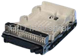
Intel FXX10DVCARBLK Enclosure - 10PK SS4000-E SPARE DR CARRIER
Request a Quote

The quote request has been received
Close

Facing challenges or have inquiries? Feel free to contact us!
Call Us +1-469-283-2440
What they say about us
FANTASTIC RESOURCE
One of our top priorities is maintaining our business with precision, and we are constantly looking for affiliates that can help us achieve our goal. With the aid of GID Industrial, our obsolete product management has never been more efficient. They have been a great resource to our company, and have quickly become a go-to supplier on our list!
Bucher Emhart Glass
EXCELLENT SERVICE
With our strict fundamentals and high expectations, we were surprised when we came across GID Industrial and their competitive pricing. When we approached them with our issue, they were incredibly confident in being able to provide us with a seamless solution at the best price for us. GID Industrial quickly understood our needs and provided us with excellent service, as well as fully tested product to ensure what we received would be the right fit for our company.
Fuji
HARD TO FIND A BETTER PROVIDER
Our company provides services to aid in the manufacture of technological products, such as semiconductors and flat panel displays, and often searching for distributors of obsolete product we require can waste time and money. Finding GID Industrial proved to be a great asset to our company, with cost effective solutions and superior knowledge on all of their materials, it’d be hard to find a better provider of obsolete or hard to find products.
Applied Materials
CONSISTENTLY DELIVERS QUALITY SOLUTIONS
Over the years, the equipment used in our company becomes discontinued, but they’re still of great use to us and our customers. Once these products are no longer available through the manufacturer, finding a reliable, quick supplier is a necessity, and luckily for us, GID Industrial has provided the most trustworthy, quality solutions to our obsolete component needs.
Nidec Vamco
TERRIFIC RESOURCE
This company has been a terrific help to us (I work for Trican Well Service) in sourcing the Micron Ram Memory we needed for our Siemens computers. Great service! And great pricing! I know when the product is shipping and when it will arrive, all the way through the ordering process.
Trican Well Service
GO TO SOURCE
When I can't find an obsolete part, I first call GID and they'll come up with my parts every time. Great customer service and follow up as well. Scott emails me from time to time to touch base and see if we're having trouble finding something.....which is often with our 25 yr old equipment.
ConAgra Foods