

 Manufacturers
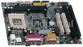
BOSER HS-2616
Description
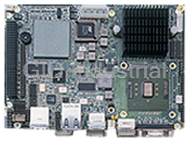
Intel Pentium M/Celeron M processor Embedded Engine Board with CF, CRT/LVDS, Dual LAN, Audio, PC/104 Plus, 4 USB2.0
Part Number
HS-2616
Price
Request Quote
Manufacturer
BOSER
Lead Time
Request Quote
Category
Single Board Computers
Specifications
System Chipset
Intel 852GME
Form Factor
Mini ITX
Ethernet Chipset
Intel 82551QM
Video Chipset
Intel 852GME
Audio
AC97 3D audio controller
BIOS
AMI PnP Flash BIOS
CF
One, Type I/II IDE interface adapter
Chipset
Intel 852GME GMCH/ICH4
CMOS
Battery backup
CPU
Intel Pentium M processor 760 2.0GHz | Intel Pentium M processor 745 1.8GHz | Intel Celeron M processor 370 1.5GHz | Intel Celeron M processor 320 1.3GHz
CPU Front Side Bus
533/400MHz FSB
Dimensions
14.5(L) x 10.2(W) cm
Ethernet
Intel 82551QM and 82562ET dual 10/100 Based LAN
I/O
8-bit input/output port (parallel)
I/O Chipset
Winbond W83627HG
IDE
One 2.0-pitch 44-pin IDE connector
IR Interface
One IrDA TX/RX header
IrDA
One IrDA TX/RX header
Keyboard/Mouse
PS/2 6-pin Mini DIN
LVDS
LVDS Panel:Supports 18-bit single channel/36-bit dual channel LVDS interface
Memory
One SO-DDR socket supports up to 1GB
PCI
PC/104 Bus connector for PCI Bus
Power In
Single +5V power in
Processor
Intel Pentium M
Serial
16C550 UART-compatible RS-232/422/485 x 1 and RS-232 x 1 serial ports with 16-byte FIFO
Temperature
0~+60°C (operating)
USB
4 USB2.0 ports, internal x 2 and external x 2
VGA
Intel 852GME for CRT display with 8MB shared main memory supports up to 1600 x 1200
Watchdog Timer
Software programmable time-out intervals from 1~255 sec.
Features
- 1 x SO-DIMM up to 1GB DDR SDRAM
- 2 x Intel 10/100 Mbps ethernet
- AC’97 audio codec
- HS-2616 provides Intel Pentium M/Celeron M processor 1.3~2.0GHz, supports 533/400MHz FSB
- HS-2616M provides ULV Intel Celeron M processor 600MHz/512K, supports 400MHz FSB
- Intel 852GM(E) GMCH/ICH4 system chipset
- Intel 852GM(E) integrated VGA for CRT & LVDS
- Supports 18-bit LVDS, 8-bit I/O, Single +5V power in, H/W Monitor function
- Supports CF, 2 x COM, 4 x USB2.0, PCI-104
Datasheet

Extracted Text
HS-2616
HS-2616M
Intel® Pentium® M/Celeron®M/
ULV Intel® Celeron® M processor
Embedded Engine Board
•CompactFlash•Mini PCI•8-bit I/O•
•CRT/LVDS•Dual LAN•Audio•
•ATA/33/66/100•RS-232/485•
•USB2.0•PCI-104•WDT•
•Single +5V•H/W Monitor•
Copyright Disclaimers
The accuracy of contents in this manual has passed thorough checking and review before
publishing. BOSER Technology Co., Ltd., the manufacturer and publisher, is not liable for
any infringements of patents or other rights resulting from its use. The manufacturer will
not be responsible for any direct, indirect, special, incidental or consequential
damages arising from the use of this product or documentation, even if advised of
the possibility of such damage(s).
This manual is copyrighted and BOSER Technology Co., Ltd. reserves all
documentation rights. Unauthorized reproduction, transmission, translation, and
storage of any form and means (i.e., electronic, mechanical, photocopying, recording)
of this document, in whole or partly, is prohibited, unless granted permission by BOSER
Technology Co., Ltd.
BOSER Technology Co., Ltd. reserves the right to change or improve the contents of
this document without due notice. BOSER Technology Co., Ltd. assumes no
responsibility for any errors or omissions that may appear in this manual, nor does
it make any commitment to update the information contained herein.
Trademarks
Trademarks
Trademarks
BOSER is a registered trademark of BOSER Technology Co., Ltd.
ISB is a registered trademark of BOSER Technology Co., Ltd.
Intel is a registered trademark of Intel Corporation.
Award is a registered trademark of Award Software, Inc.
AMI is a registered trademark of AMI Software, Inc.
All other trademarks, products and or product names mentioned herein are
mentioned for identification purposes only, and may be trademarks and/or
registered trademarks of their respective companies or owners.
© Copyright 2007 BOSER Technology Co., Ltd.
All Rights Reserved.
Edition 1.4, October 15, 2009
Table of Contents
Chapter 1 General Description ..................................1
1.1 Major Features....................................................................... 2
1.2 Specifications ........................................................................ 2
1.3 Board Dimensions................................................................. 4
Chapter 2 Unpacking..................................................5
2.1 Opening the Delivery Package............................................. 5
2.2 Inspection............................................................................... 5
Chapter 3 Hardware Installation ..............................7
3.1 Before Installation ................................................................. 7
3.2 Board Layout ......................................................................... 8
3.3 Jumper List ............................................................................ 9
3.4 Connector List ....................................................................... 9
3.5 Configuring the CPU ........................................................... 10
3.6 System Memory................................................................... 10
3.7 VGA Controller .................................................................... 10
3.8 PCI E-IDE Drive Connector................................................. 12
3.9 Serial Port Connectors ....................................................... 13
3.10 Ethernet Connector............................................................. 14
3.11 USB Port............................................................................... 14
3.12 CMOS Data Clear................................................................. 15
3.13 Power and Fan Connectors................................................ 15
3.14 Keyboard/Mouse Connectors ............................................ 16
3.15 System Front Panel Control............................................... 16
Connector JP1 Orientation .....................................................................................16
3.16 Watchdog Timer .................................................................. 17
3.17 Audio Connectors ............................................................... 18
3.18 CompactFlash Connector................................................ 18
3.19 IrDA Function....................................................................... 20
3.20 8-bit I/O Function................................................................. 20
3.21 PCI-104 Connector .............................................................. 24
Chapter 4 AMI BIOS Setup.....................................27
4.1 Starting Setup...................................................................... 27
4.2 Using Setup ......................................................................... 28
4.3 Main Menu............................................................................ 29
4.4 Advanced Settings.............................................................. 30
4.5 Advanced PCI/PnP Settings............................................... 33
4.6 Boot Settings....................................................................... 34
4.7 Security Settings ................................................................. 35
4.8 Advanced Chipset Settings................................................ 36
4.9 Exit Options ......................................................................... 37
Chapter 5 Software Utilities.....................................39
5.1 IDE Driver Installation......................................................... 39
5.2 VGA Driver Installation ....................................................... 43
5.3 LAN Driver Installation........................................................ 52
5.4 Audio Driver Installation..................................................... 65
5.5 USB2.0 Driver Installation .................................................. 68
Safety Instructions
Integrated circuits on computer boards are sensitive to static electricity. To
avoid damaging chips from electrostatic discharge, observe the following
precautions:
� Do not remove boards or integrated circuits from their anti-static packaging
until you are ready to install them.
� Before handling a board or integrated circuit, touch an unpainted portion of
the system unit chassis for a few seconds. This helps to discharge any static
electricity on your body.
� Wear a wrist-grounding strap, available from most electronic component
stores, when handling boards and components. Fasten the ALLIGATOR clip
of the strap to the end of the shielded wire lead from a grounded object.
Please wear and connect the strap before handle the product to ensure
harmlessly discharge any static electricity through the strap.
� Please use an anti-static pad when putting down any components or parts or
tools outside the computer. You may also use an anti-static bag instead of
the pad. Please inquire from your local supplier for additional assistance in
finding the necessary anti-static gadgets.
NOTE: DO NOT TOUCH THE BOARD OR ANY OTHER SENSITIVE
COMPONENTS WITHOUT ALL NECESSARY ANTI-STATIC
PROTECTIONS.
Chapter 1
General Description
HS-2616 HS-2616M
The HS-2616 is an Intel® 852GME GMCH and HS-2616M is an Intel®
852GM GMCH chipset-based board designed. The HS-2616/
HS-2616M is ideal all-in-one embedded engine board. Additional
features include an enhanced I/O with CF, CRT/LVDS, dual LAN,
audio, 4 COM, and USB2.0 interfaces.
Its onboard ATA/33/66/100 to IDE drive interface architecture allows
the HS-2616/HS-2616M to support data transfers of 33, 66 or
100MB/sec. to one IDE drive connection. The HS-2616 supports Intel®
Pentium® M/Celeron® M processor, and HS-2616M supports ULV
Intel® Celeron® M processor 600MHz/512K.
The Intel® 852GM with 8MB shared main memory supporting CRT
display up to 1600 x 1200. It also supports 18-bit single/dual-channel
LVDS interface.
System memory is also sufficient with the one SO-DDR socket that can
support up to 1GB.
Additional onboard connectors include four USB2.0 ports providing
faster data transmission. And two external RJ-45 connectors for
10/100 Based Ethernet use.
1
To ensure the reliability in an unmanned or standalone system, the
watchdog timer (WDT) onboard HS-2616/HS-2616M is designed with
software that does not need the arithmetical functions of a real-time
clock chip. If any program causes unexpected halts to the system, the
onboard WDT will automatically reset the CPU or generate an interrupt
to resolve such condition.
1.1 Major Features
The HS-2616/HS-2616M comes with the following features:
� HS-2616 provides Intel® Pentium® M/Celeron® M processor
1.3~2.0GHz, supports 533/400MHz FSB
� HS-2616M provides ULV Intel® Celeron® M processor 600MHz/512K,
supports 400MHz FSB
� 1 x SO-DIMM up to 1GB DDR SDRAM
� Intel® 852GM(E) GMCH/ICH4 system chipset
� Intel® 852GM(E) integrated VGA for CRT & LVDS
� 2 x Intel® 10/100 Mbps ethernet
� AC’97 audio codec
� Supports CF, 2 x COM, 4 x USB2.0, PCI-104
� Supports 18-bit LVDS, 8-bit I/O, Single +5V power in, H/W Monitor
function
1.2 Specifications
� System
� CPU
HS-2616 provides
Intel® Pentium® M processor 760 2.0GHz
Intel® Pentium® M processor 745 1.8GHz
Intel® Celeron® M processor 370 1.5GHz
Intel® Celeron® M processor 320 1.3GHz
HS-2616M provides ULV Intel® Celeron® M processor 600MHz/512K
� Front Side Bus
533/400MHz FSB (HS-2616)
400MHz FSB (HS-2616M)
� BIOS
AMI PnP Flash BIOS
� System Chipset:
Intel® 852GME GMCH/ICH4 (HS-2616)
Intel® 852GM GMCH/ICH4 (HS-2616M)
� I/O Chipset
Winbond W83627HG
2
� System Memory
1 x 200-pin SO-DIMM socket up to 1GB DDR SDRAM
� Storage
1 x Type II CF socket
� Watchdog Timer
Software programmable time-out intervals from 1~255 sec. or 1~255
min.
� Hardware Monitor
Monitoring temperatures, voltages, and cooling fan status
� Expansion
PCI-104
� Power In
Single +5V power in
� Operating Temperature
0~+60 degrees C
� Operating Humidity
0~95%, non-condensing
� Board Size (L x W)
145 x 102 mm
� I/O Interface
� MIO
1 x RS-232
1 x RS-232/485
4 x USB2.0 (2 x internal, 2 x external)
1 x IDE
1 x PS/2 for KB/MS
� DI/O
8-bit input/output by parallel port
� Display
� Chipset
Intel® 852GME (HS-2616)
Intel® 852GM (HS-2616M)
� Display Memory
8MB shared main memory
� LVDS
18-bit single/dual-channel
� Resolution
CRT Mode: 1600 x 1200
� Audio
� Chipset
RealTek ALC202A
� Audio Interface (w/pin header)
MIC In, Line Out
3
� Ethernet
� Chipset
Intel® 82551QM and 82562ET dual 10/100 Mbps LAN
� Ethernet Interface
2 x RJ-45
1.3 Board Dimensions
4
Chapter 2
Unpacking
2.1 Opening the Delivery Package
The HS-2616/HS-2616M is packed in an anti-static bag. The board has
components that are easily damaged by static electricity. Do not
remove the anti-static wrapping until proper precautions have been
taken. Safety Instructions in front of this manual describe anti-static
precautions and procedures.
2.2 Inspection
After unpacking the board, place it on a raised surface and carefully
inspect the board for any damage that might have occurred during
shipment. Ground the board and exercise extreme care to prevent
damage to the board from static electricity.
Integrated circuits will sometimes come out of their sockets during
shipment. Examine all integrated circuits, particularly the BIOS,
processor, memory modules, ROM-Disk, and keyboard controller chip
to ensure that they are firmly seated. The HS-2616/HS-2616M delivery
package contains the following items:
� HS-2616 or HS-2616M Board x 1
� Utility CD Disk x 1, including User’s Manual
� Cables (as following table)
� Jumper Bag x 1
5
Cables Package
NO. Description QTY.
1 1-to-2 Mini DIN cable 1
2 SPK 8-pin(2.0-pitch) phone jack x 2 1
3 COM DB9-10P (2.0-pitch) 1
4 40-pin to 44-pin IDE flat cable 1
It is recommended that you keep all the parts of the delivery package
intact and store them in a safe/dry place for any unforeseen event
requiring the return shipment of the product. In case you discover any
missing and/or damaged items from the list of items, please contact
your dealer immediately.
Option Accessories
NO. Description
1 1-to-2 USB cable with bracket
2 Pentium® M Cooler (251-10310003G)
6
Chapter 3
Hardware Installation
This chapter provides the information on how to install the hardware
using the HS-2616/HS-2616M. This chapter also contains information
related to jumper settings of switch, and watchdog timer selection etc.
3.1 Before Installation
After confirming your package contents, you are now ready to install
your hardware. The following are important reminders and steps to
take before you begin with your installation process.
1. Make sure that all jumper settings match their default settings
and CMOS setup correctly. Refer to the sections on this chapter
for the default settings of each jumper. (set JP7 1-2)
2. Go through the connections of all external devices and make
sure that they are installed properly and configured correctly
within the CMOS setup. Refer to the sections on this chapter
for the detailed information on the connectors.
3. Keep the manual and diskette in good condition for future
reference and use.
7
3.2 Board Layout
Top Side
Solder Side
8
3.3 Jumper List
Jumper Default Setting Setting Page
Onboard LAN 2 Enabled/Disabled Select:
JP3 Short 1-2 14
Enabled
JP4 COM2 Use RS-232 or RS-485 Select: RS-232 Open 13
JP5 Short 3-4 10
System Frequency Select: 400MHz
JP10 Short 10
JP7 Clear CMOS: Normal Operation Short 1-215
JP11 SDRAM Frequency Select: 266MHz Short 1-210
3.4 Connector List
Connector Definition Page
CN1 PCI-104 Connector 24
CN3/CN2 COM 1/COM 2 Connector (5x2 header) 13
CN4 Internal USB2.0 Port 14
CN5 IDE Connector 12
CN6 External Reset Button 16
CN7 External USB2.0 Port 14
CN8 RS-485 Connector 13
CN9 MIC In/Line Out Connector 18
CN10/CN11 RJ-45 Connector 14
CN12 PS/2 6-pin Mini DIN KB/MS Connector 16
CN13 15-pin CRT Connector 10
CN15/CN14 LVDS Panel Connector 10
CN16 IrDA Connector 20
CN17 SO-DDR Socket 10
CN18 CompactFlash Connector 18
FN1 Fan Power In Connector 15
JP1 System Front Panel Control 16
JP2 8-bit I/O Connector 20
JP6 Inverter Power In Connector 10
PW1 4-pin Power In Connector 15
9
3.5 Configuring the CPU
The HS-2616 provides Intel® Pentium® M processor 760 2.0GHz,
Pentium® M processor 745 1.8GHz, Celeron® M processor 370
1.5GHz, and Celeron® M processor 1.3GHz. The HS-2616M
embedded with ULV Intel® Celeron® M processor 600MHz/512K. If
you want to use 533MHz FSB processor, please set JP5/JP10, and
JP5/JP10 is only for HS-2616.
� JP5/JP10: System Frequency Select
Settings
Options
JP5 JP10
400MHz FSB (default) Short 3-4 Short
533MHz FSB All Open Open
3.6 System Memory
The HS-2616/HS-2616M provides one SO-DDR socket at locations
CN17. The maximum capacity of the onboard memory is 1GB.
NOTE: If System Frequency sets 400MHz FSB, please use 266MHz SDRAM
� JP11: SDRAM Frequency Select
Options Settings
1
333MHz FSB Open
2
266MHz FSB (default) Short
3.7 VGA Controller
The HS-2616/HS-2616M provides two connection methods of a VGA
device. CN13 offers a single standard CRT connector and CN15/CN14
are the LVDS interface connectors onboard reserved for flat panel
installation.
10
� CN13: CRT Connector
PIN Description PIN Description
1 Red 2 Green
3 Blue 4 N/C
6 11
1
5 GND 6 GND
7 GND 8 GND
9 N/C 10 GND
11 N/C 12 SDA
10
5
15
13 HSYNC 14 VSYNC
15 SCL
� CN15/CN14: LVDS Interface Connector
PIN Description PIN Description
12
1 V 2 V
LCD LCD
3 GND 4 GND
5 A0-/A4- 6 A0+/A4+
7 A1-/A5- 8 A1+/A5+
9 A2-/A6- 10 A2+/A6+
13 14
11 CLK1-/CLK2- 12 CLK1+/CLK2+
13 N/C 14 N/C
NOTE: LVDS cable should be produced very carefully. A0- & A0+ have to
be fabricated in twister pair (A1- & A1+, A2- & A2+ and so on)
otherwise the signal won’t be stable.
NOTE: If use CN15 only, it just supports 18-bit single channel LVDS
panel; If you want to use 36-bit dual channel LVDS panel, please
use CN15 and CN14 combined.
� JP6: Inverter Power In Connector
PIN Description
1
1 +12V
2 +12V
3 VCC5
4 BK_EN
6
5 LCD_EN
6 GND
11
3.8 PCI E-IDE Drive Connector
CN5 is a standard 44-pin 2.0-pitch connector daisy-chain driver
connector serves the PCI E-IDE drive provisions onboard the HS-2616/
HS-2616M. A maximum of two ATA/33/66/100 IDE drives can be
connected to the HS-2616/HS-2616M via CN5.
� CN5: IDE Connector
PIN Description PIN Description
1 Reset 2 GND
3 DATA 7 4 DATA 8
5 DATA 6 6 DATA 9
7 DATA 5 8 DATA 10
9 DATA 4 10 DATA 11
11 DATA 3 12 DATA 12
13 DATA 2 14 DATA 13
15 DATA 1 16 DATA 14
17 DATA 0 18 DATA 15
19 GND 20 N/C
21 PDREQ 22 GND
23 IOW# 24 GND
25 IOR# 26 GND
27 PIORDY 28 PR1PD1-
29 RPDACK- 30 GND
31 Interrupt 32 N/C
33 RPDA1- 34 PATA66
35 RPDA0- 36 RPDA2-
37 RPCS1- 38 RPCS3-
39 HDD Active 40 GND
41 VCC 42 VCC
43 GND 44 N/C
43 1
44
2
12
3.9 Serial Port Connectors
The HS-2616/HS-2616M offers NS16C550 compatible UARTs
with Read/ Receive 16-byte FIFO serial ports and internal 10-pin
headers and RS-422/485 connector.
� CN3/CN2: COM 1/COM 2 Connector (5x2 Header)
PIN Description PIN Description
1 DCD 2 DSR
9 1
3 RXD 4 RTS
5 TXD 6 CTS
10 2
7 DTR 8 RI
9 GND 10 N/C
� CN8: RS-485 Connector (3x2 Header, COM4)
PIN Description PIN Description
5 1
1 TX- 2 TX+
3 RX+ 4 RX-
62
5 GND 6 VCC
NOTE: The terminal resistance of RX & TX is set at 180Ω.
� JP4: COM 2 use RS-232 or RS-485 Select
Options Settings
9 1
RS-232 (default) Open
RS-485 by Auto (*1) Short 1-2, 3-4, 5-7, 8-10
10 2
RS-485 by –RTS (*-1) Short 1-2, 3-4, 7-9, 8-10
RS-485 Full Duplex (*2) Short 1-2, 3-4, 6-8
NOTE: *1: 2-wires RS-485 function
*2: 4-wires point-to-point full duplex function
4-wires point-to-point full duplex RS-485
13
Typical RS-485 2-wires Mutildrop Network
3.10 Ethernet Connector
The HS-2616/HS-2616M provides two external RJ-45 interface
connectors. Please refer to the following for its pin information.
� CN10/CN11: RJ-45 Connector
PIN Description
1 TX+
2 TX-
3 RX+
4 R/C GND
8 1
5 R/C GND
6 RX-
7 R/C GND
8 R/C GND
� JP3: Onboard LAN 2 Enabled/Disabled Select
Options Settings
1
Enabled (default) Short 1-2
3
Disabled Short 2-3
3.11 USB Port
The HS-2616/HS-2616M provides one 8-pin connectors, at location
CN4, for two USB ports, and four external USB2.0 ports at CN7.
� CN7: External USB2.0 Port
PIN Description PIN Description
1 VCC 2 VCC
3 USBD0- 4 USBD1-
5 USBD0+ 6 USBD1+
7 GND 8 GND
14
� CN4: Internal USB2.0 Port
PIN Description PIN Description
1 2
1 VCC 2 VCC
3 USBD2- 4 USBD3-
78
5 USBD2+ 6 USBD3+
7 GND 8 GND
3.12 CMOS Data Clear
The HS-2616/HS-2616M has a Clear CMOS jumper on JP7.
� JP7: Clear CMOS
Options Settings 1
Normal Operation (default) Short 1-2
3
Clear CMOS Short 2-3
IMPORTANT: Before you turn on the power of your system, please
set JP7 to Short 1-2 for normal operation.
3.13 Power and Fan Connectors
HS-2616/HS-2616M provides one 4-pin power in at PW1.
� PW1: 4-pin Power In Connector
PIN Description
4
1 VCC
2 GND
3 GND
4 +12V
1
� FN1: Fan Power In Connector
PIN Description
1 GND
13
2 +5V
3 Fan Speed
15
3.14 Keyboard/Mouse Connectors
The HS-2616/HS-2616M offers CN12 for an internal 6-pin cable
converter to keyboard/mouse.
� CN12: 6-pin Keyboard/Mouse Connector
PIN Description
1 Keyboard Data
6
2 Mouse Data
3 GND
4 VCC
1
5 Keyboard Clock
6 Mouse Clock
3.15 System Front Panel Control
The HS-2616/HS-2616M has system front panel control at location
JP1.
� JP1: System Front Panel Control
PIN Description PIN Description
1 VCC 2 Speaker
3 HDD LED 4 N/C
5 N/C 6 GND
7 N/C 8 VCC
9 Reset Switch 10 VCC
11 GND 12 GND
Connector JP1 Orientation
1 2
HDD LED
3 4
Speaker
5 6
7 8
9 10
Reset
PWR LED
Button
11 12
16
� CN6: External Reset Button
PIN Description
1 GND
3 4
2 Reset Switch
12
3 GND
4 GND
3.16 Watchdog Timer
Once the Enable cycle is active a Refresh cycle is requested before the
time-out period. This restarts counting of the WDT period. When the
time counting goes over the period preset of WDT, it will assume that
the program operation is abnormal. A system reset signal will restart
when such error happens.
The following sample programs show how to enable, disable and
refresh the watchdog timer:
;----------------------------------------------------------------
;Enter the WDT function mode, interruptible double-write
;----------------------------------------------------------------
MOV DX, 2EH
MOV AL, 87H
OUT DX, AL
OUT DX, AL
MOV DX, 2EH
MOV AL, 07H
OUT DX, AL
MOV DX, 2FH
MOV AL, 08H
OUT DX, AL
MOV DX, 2EH
MOV AL, F5H
OUT DX, AL ;select CRF0
MOV DX, 2FH
MOV AL, 80H
OUT DX, AL
MOV DX, 2EH
MOV AL, F7H
OUT DX, AL
MOV DX, 2FH
MOV AL, 00H
OUT DX, AL
MOV DX, 2EH
MOV AL, F6H
OUT DX, AL
MOV DX, 2FH
MOV AL, 00H ; *00H=Disabled
OUT DX, AL
17
;----------------------------------------------------------------
;Exit extended function mode
;----------------------------------------------------------------
MOV DX, 2EH
MOV AL, AAH
OUT DX, AL
User can also use AL, 00H’s defined time for reset purposes, e.g.00H
for Disable, 01H = 1sec, 02H=2sec….FFH=255sec.
3.17 Audio Connectors
The HS-2616 has an onboard AC97 3D audio controller. The following
tables list the pin assignments of the Line In/Audio Out connector.
� CN9: MIC In/Line Out Connector
PIN Description PIN Description
1 AOUTL 2 AOUTR
1 2
3 GND 4 GND
78
5 MIC IN 6 N/C
7 GND 8 GND
3.18 CompactFlash Connector
The HS-2616/HS-2616M also offers a Type I/II CompactFlash
connector which is IDE interface located at the solder side of the board.
The designated CN18 connector, once soldered with an adapter, can
hold CompactFlash cards of various sizes. Please turn off the power
before inserting the CF card.
� CN18: CompactFlash Connector
PIN Description PIN Description
1 GND 2 IDE_PDD3
3 IDE_PDD4 4 IDE_PDD5
5 IDE_PDD6 6 IDE_PDD7
7 IDE_PDCS1# 8 GND
9 GND 10 GND
11 GND 12 GND
13 +3.3V 14 GND
15 GND 16 GND
17 GND 18 IDE_PDA2
19 IDE_PDA1 20 IDE_PDA0
…MORE ON NEXT PAGE…
18
PIN Description PIN Description
21 IDE_PDD0 22 IDE_PDD1
23 IDE_PDD2 24 GND
25 GND 26 GND
27 IDE_PDD11 28 IDE_PDD12
29 IDE_PDD13 30 IDE_PDD14
31 IDE_PDD15 32 IDE_PDCS3#
33 GND 34 IDE_PDIOR#
35 IDE_PDIOW# 36 +3.3V
37 INT_IRQ15 38 +3.3V
39 +3.3V 40 N/C
41 RESET# 42 IDE_PDIORDY
43 CF_PDERQ 44 CF_REGB
45 IDE_ACTP# 46 DETECT
47 IDE_PDD8 48 IDE_PDD9
49 IDE_PDD10 50 GND
Inserting a CompactFlash card into the adapter is not a difficult task.
The socket and card are both keyed and there is only one direction for
the card to be completely inserted. Refer to the diagram on the
following page for the traditional way of inserting the card.
19
CompactFlash
PCB Solder
Side Vi
ew
CE
TM
CF Rear Side
Made in Japan /
Fabrique Au Japon
3.19 IrDA Function
CN16 is a 5-pin internal IR communication connector for connection of
an IrDA device.
� CN16: IrDA Connector
PIN Description
1 VCC 1
2 N/C
3 IRRX
4 GND 5
5 IRTX
3.20 8-bit I/O Function
The HS-2616/HS-2616M offers one 8-bit input/output port by parallel
port.
� JP2: 8-bit Input/Output
PIN Description PIN Description
1 VCC 2 GND
9 1
3 GD0 4 GD4
5 GD1 6 GD5
10 2
7 GD2 8 GD6
9 GD3 10 GD7
.286
.MODEL SMALL
.DATA ;this is data area
port equ 0378h ;print port can be change to 278h
.CODE
print macro buff
mov dx, offset buff;
mov ah,09h
int 21h
endm
delay :
push cx
mov cx,0155h
@@:
jmp $+2
push cx
mov cx,0ffffh
20
wait1: loop wait1
pop cx
loop @b
pop cx
ret
begin proc near
mov ax,@data
mov ds,ax
STI
Mov dx, port
Mov al, 80h out dx, al
;;--------------------
;;ROR
mov cx, 08h
@@:
ror al, 1
call delay
out dx, al
loop @b
pop cx
;;ROL
push cx
mov cx, 08h
@@:
rol al, 1
out dx, al
call delay
loop @b
pop cx
;;--------------------
;;--------------------
;;ROR
mov cx, 08h
@@:
ror al, 1
call delay
out dx, al
loop @b
pop cx
;;ROL
push cx
mov cx, 08h
@@:
rol al, 1
out dx, al
call delay
loop @b
pop cx
;;--------------------
;;--------------------
;;ROR
mov cx, 08h
@@:
ror al, 1
21
call delay
out dx, al
loop @b
pop cx
;;ROL
push cx
mov cx, 08h
@@:
rol al, 1
out dx, al
call delay
loop @b
pop cx
;;--------------------
;;--------------------
;;ROR
mov cx, 08h
@@:
ror al, 1
call delay
out dx, al
loop @b
pop cx
;;ROL
push cx
mov cx, 08h
@@:
rol al, 1
out dx, al
call delay
loop @b
pop cx
;;--------------------
;;--------------------
;;ROR
mov cx, 08h
@@:
ror al, 1
call delay
out dx, al
loop @b
pop cx
;;ROL
push cx
mov cx, 08h
@@:
rol al, 1
out dx, al
call delay
loop @b
pop cx
;;--------------------
;;--------------------
;;ROR
mov cx, 08h
@@:
ror al, 1
call delay
22
out dx, al
loop @b
pop cx
;;ROL
push cx
mov cx, 08h
@@:
rol al, 1
out dx, al
call delay
loop @b
pop cx
;;--------------------
;;--------------------
;;ROR
mov cx, 08h
@@:
ror al, 1
call delay
out dx, al
loop @b
pop cx
;;ROL
push cx
mov cx, 08h
@@:
rol al, 1
out dx, al
call delay
loop @b
pop cx
;;--------------------
;flash LED 3 time
mov cx, 01h
@@:
mov al, 0ffh
out dx, al
call delay
mov al,0h
out dx, al
call delay
loop @b
ee:
mov ah, 4ch ;go back to dos
int 21h
.stack
begin endp
end begin
23
3.21 PCI-104 Connector
The HS-2616/HS-2616M provides one PCI-104 connector, at location
CN1.
NOTE: To integrate the PCI-104 module on to the HS-2616/HS-2616M,
please use the enclosed 17mm copper stand-off to raise
up the module board.
� CN1: PCI-104 Connector
PIN Description PIN Description
A1 N/C B1 N/C
A2 N/C B2 AD2
A3 AD5 B3 GND
A4 CBE0# B4 AD7
A5 GND B5 AD9
A6 AD11 B6 N/C
A7 AD14 B7 AD13
A8 +3.3V B8 CBE1#
A9 SERR# B9 GND
A10 GND B10 PERR#
A11 STOP# B11 +3.3V
A12 +3.3V B12 TRDY-
A13 FRAME# B13 GND
A14 GND B14 AD16
A15 AD18 B15 +3.3V
A16 AD21 B16 AD20
A17 +3.3V B17 AD23
A18 IDSEL0 B18 GND
A19 AD24 B19 CBE3#
A20 GND B20 AD26
A21 AD29 B21 VCC
A22 VCC B22 AD30
A23 REQ0# B23 GND
A24 GND B24 REQB
A25 GNTA B25 N/C
A26 VCC B26 PCICLK8
A27 PCICLKB B27 VCC
…MORE ON NEXT PAGE…
24
D1
C1
B1
A1
PIN Description PIN Description
A28 GND B28 INTR_D#
A29 +12V B29 INTR_A#
A30 -12V B30 REQC
C1 VCC D1 AD0
C2 AD1 D2 VCC
C3 AD4 D3 AD3
C4 GND D4 AD6
C5 AD8 D5 GND
C6 AD10 D6 PULL VCC
C7 GND D7 AD12
C8 AD15 D8 +3.3V
C9 N/C D9 PAR
C10 +3.3V D10 PULL VCC
C11 PULL VCC D11 GND
C12 GND D12 DEVSEL#
C13 IRDY# D13 +3.3V
C14 +3.3V D14 CBE2#
C15 AD17 D15 GND
C16 GND D16 AD19
C17 AD22 D17 +3.3V
C18 IDSEL1 D18 IDSEL2
C19 N/C D19 IDSEL3
C20 AD25 D20 GND
C21 AD28 D21 AD27
C22 GND D22 AD31
C23 REQA D23 N/C
C24 VCC D24 GNT0#
C25 GNTB D25 GND
C26 GND D26 PCICLKA
C27 PCICLKC D27 GND
C28 VCC D28 PCIRST#
C29 INTR_B# D29 INTR_C#
C30 INTR_C# D30 N/C
25
This page is the blank page.
26
Chapter 4
AMI BIOS Setup
The HS-2616 uses AMI BIOS for the system configuration. The AMI
BIOS setup program is designed to provide the maximum flexibility in
configuring the system by offering various options that could be
selected for end-user requirements. This chapter is written to assist
you in the proper usage of these features.
4.1 Starting Setup
The AMI BIOS is immediately activated when you first power on the
computer. The BIOS reads the system information contained in the
CMOS and begins the process of checking out the system and
configuring it. When it finishes, the BIOS will seek an operating system
on one of the disks and then launch and turn control over to the
operating system.
While the BIOS is in control, the Setup program can be activated in one
of two ways:
1. By pressing immediately after switching the system on, or
2. By pressing the key when the following message appears
briefly at the bottom of the screen during the POST (Power On Self
Test).
Press DEL to enter SETUP.
If the message disappears before you respond and you still wish to
enter Setup, restart the system to try again by turning it OFF then ON or
pressing the "RESET" button on the system case. You may also restart
by simultaneously pressing
Frequently asked questions
How does Industrial Trading differ from its competitors?

Is there a warranty for the HS-2616?
Which carrier will Industrial Trading use to ship my parts?
Can I buy parts from Industrial Trading if I am outside the USA?
Which payment methods does Industrial Trading accept?
Why buy from GID?

Quality
We are industry veterans who take pride in our work

Protection
Avoid the dangers of risky trading in the gray market

Access
Our network of suppliers is ready and at your disposal

Savings
Maintain legacy systems to prevent costly downtime

Speed
Time is of the essence, and we are respectful of yours
Related Products

Boser 251-10301001 CPU Board with 1U high CPU cooler for PGA 478 1.7~2.4GHz CPU for HS-4701
Pentium II/III Slot 1 Full-size Board with VGA & LAN

Intel Pentium 4 processor PICMG Bus SBC with VGA, Audio, Dual LAN & USB2.0
Intel Pentium 4 processor PICMG Bus SBC with VGA, Audio, Dual LAN & USB2.0
Request a Quote

The quote request has been received
Close

Facing challenges or have inquiries? Feel free to contact us!
Call Us +1-469-283-2440
What they say about us
FANTASTIC RESOURCE
One of our top priorities is maintaining our business with precision, and we are constantly looking for affiliates that can help us achieve our goal. With the aid of GID Industrial, our obsolete product management has never been more efficient. They have been a great resource to our company, and have quickly become a go-to supplier on our list!
Bucher Emhart Glass
EXCELLENT SERVICE
With our strict fundamentals and high expectations, we were surprised when we came across GID Industrial and their competitive pricing. When we approached them with our issue, they were incredibly confident in being able to provide us with a seamless solution at the best price for us. GID Industrial quickly understood our needs and provided us with excellent service, as well as fully tested product to ensure what we received would be the right fit for our company.
Fuji
HARD TO FIND A BETTER PROVIDER
Our company provides services to aid in the manufacture of technological products, such as semiconductors and flat panel displays, and often searching for distributors of obsolete product we require can waste time and money. Finding GID Industrial proved to be a great asset to our company, with cost effective solutions and superior knowledge on all of their materials, it’d be hard to find a better provider of obsolete or hard to find products.
Applied Materials
CONSISTENTLY DELIVERS QUALITY SOLUTIONS
Over the years, the equipment used in our company becomes discontinued, but they’re still of great use to us and our customers. Once these products are no longer available through the manufacturer, finding a reliable, quick supplier is a necessity, and luckily for us, GID Industrial has provided the most trustworthy, quality solutions to our obsolete component needs.
Nidec Vamco
TERRIFIC RESOURCE
This company has been a terrific help to us (I work for Trican Well Service) in sourcing the Micron Ram Memory we needed for our Siemens computers. Great service! And great pricing! I know when the product is shipping and when it will arrive, all the way through the ordering process.
Trican Well Service
GO TO SOURCE
When I can't find an obsolete part, I first call GID and they'll come up with my parts every time. Great customer service and follow up as well. Scott emails me from time to time to touch base and see if we're having trouble finding something.....which is often with our 25 yr old equipment.
ConAgra Foods