��������
�����������������
�����������������
������������������
���������� �!�
�
����!�������
��������������������������������������������������������������������������
������������������������������ ������������������!�������������������
������"����������!������������������"�������������!�������#����������������
��������������
�����������������������!��������������������������������������������
�������������������������������������������������������������!�����
���������!���������������������������������������������������
������������������������"�������������!���������������������������
���$���!�����������������������#���������������
%��!������������������������������!���������������������������������������
���������������������������������������������������������������������
!������!���"����������"����������#�����#�����������!�����#�������!����������
����������������� ����
�������������������������������������
���������������������
�� �����!��"����� ��#�
$�� ����� ��%�&% �
���������������������������
AXIOMTEK is a trademark of AXIOMTEK Co., Ltd.
ALi is a trademark of Acer Laboratories, Inc.
AMD is a trademark of Advanced Micro Devices, Inc.
Award is a trademark of Award Software, Inc.
IBM, PC/AT, PS/2, VGA are trademarks of International
Business Machines Corporation.
C&T is a trademark of Chips and Technologies, Inc.
Realtek RTL-8139C is a registered trademark of Realtek
Semiconductor Corporation.
Other brand names and trademarks are the properties
and
registered brands of their respective owners.
���
�
��������������������������������
Chapter 1 Chapter 1 Chapter 1 Chapter 1 Introducti Introducti Introducti Introduction on on on
���� ������������������������������������������������������������������������
���� �������������� ��������������������������������������������������������������
���� ��������������������������������������������������������������������������
Chapter 2 Chapter 2 Chapter 2 Chapter 2 Installati Installati Installati Installation on on on
���� �������������������������������� �����������������������������
���� ���������������������������������������������������������������������������� �
���� !�����������������������������������������������������������������������"�
2.3.1 Watchdog Function Setting: JP1 ............................. 7
2.3.2 Serial Ports Settings: JP2, JP3, JP7............................ 8
2.3.3 CMOS Clear Jumper: JP4......................................... 8
2.3.4 Flat Panel Voltage Selection: JP5 ........................... 8
2.3.5 DiskOnChip Memory Segment: JP6 ....................... 9
��#� $��������������������������������������������������������������������������%�
Chapter 3 Chapter 3 Chapter 3 Chapter 3 Hardware Hardware Desc Hardware Desc Hardware Desc Descriptio riptio riptio ription nn n
���� �����&�������������������������������������������������������������������
���� $�� �����������������������������������������������������������������������������
���� �’(�����������������������������������������������������������������������������
��#� �&�����)����&�����������������������������������������������������������
���� ’*(������+�������)����������������������������������������������������
�� � ’���������$��������������������������������������������������������������
��"� ��������(������$������������������������������������������������#�
��,� ’�-�’���������$������������������������������������������������������
��%� ������&�’��������������������������������������������������������������� �
3.9.1 Flat Panel/CRT Interface Controller ...................... 16
3.9.2 Features..................................................................16
3.9.3 VGA/Flat Panel Connectors .................................. 17
3.9.4 Flat Panel Connector Pin Description ................... 18
���.� �����&����/�$�������������������������������������������������������%�
����� ��������������’�������������������������������������������������������.�
����� ������������’������������������������������������������������������������
����� 0����1����$���/�����$)(��0+)��������������������������������
���#� 2�&3�����������*��)�����$��������������������������������
Table of Contents
����
�
����� -�4������$�������������������������������������������������������������
��� � $�������$�������������������������������������������������������������
���"� ’��+�$�������� �����������������������������������������������������������
���,� ��5���’�����$��������� �������������������������������������������#�
���%� 6+7�6-���������������������������������������������������������������������#�
���.� �$*�.#�$��������� ���������������������������������������������������#�
Chapt Chapt Chapt Chapter 4 er 4 e er 4 r 4 Displa Displa Displa Display Drivers y Drivers y y Drivers Drivers
#��� 8����5������������������������������������������������������������������,�
#��� 8����5��71������������������������������������������������������������.�
#��� (�*������������������������������������������������������������������������������
#�#� 9�+�����5������������� ����������������������������������������������#�
4.4.1 DOS Utility................................................................34
4.4.2 Windows 95 Utility ................................................... 35
4.4.3 Windows 3.1 Utility .................................................. 37
4.4.4 Setup Programs......................................................39
Chapter 5 Chapter 5 E Etthernet Introducti hernet Introduction on
Chapter 5 Chapter 5 E Et thernet Introducti hernet Introduction on
���� ’�������������������������������������������������������������������������#��
���� ���������������������������������������������������������������������������#��
���� ���:�����������������������������������������������������������������#��
Chapter 6 Chapter 6 Chapter 6 Chapter 6 Aw Aw Aw Award BIOS ard BIOS ard BIOS ard BIOS Uti Uti Uti Util l l liiiit t t ty y y y
��� -����������������������������������������������������������������������#��
��� $�������2�&� ������������������������������������������������������������# �
��� �������������������������������������������������������������������������# �
�#� )����)�������������������������������������������������������������������#"�
��� ���������$)(�����������������������������������������������������#%�
� � �’(�������������������������������������������������������������������
�"� $4�����������������������������������������������������������������%�
�,� ��5���)������������������������������������������������������� .�
�%� �$’�$������������������������������������������������������������ #�
��.� 6�����’(������������������������������������������������������������ "�
���� 6������������������������������������������������������������������� ,�
���� ����5���������������������������������������������������������������� ,�
���� ’�-�����+������������� ������������������������������������������ %�
��#� ��:��;�-��������������������������������������������������������������"��
���� -����8��4������:��� �������������������������������������������������"��
�� � �’(��0���������<��(�1�$���� ��������������������������������"#�
���
Table of Contents
�
Ap Ap Ap App p p pe e e en n n nd d d diiiix x x x A A A A Watchdog Watchdog Ti Watchdog Ti Watchdog TiTim mm me ee er rr r
�������4��8���4������������ ������������������������������������������"%�
�
Table of Contents
��
SBC8440 3.5� Form Factor SBC User’s Manual
�
�����������������
�������������
"�"� #�����!�������$�����
�
����������������������������������������������������������
������������������������������������ ��������!������������
"�����#�$�%����� �����"�����������������&’(��!)))��*+,�+-’�
,�����������������������������.��������������������/��������.�
���.���������������0��121�������3����"���0�121������"���
0�1214�114��)5����������� �����������������������������(�’�
���������’�6���������.������������"�����"���������.�������������
������������������#�7����������������������������������"�
��������������������������������� ����������������������
�����������������������#�
Introduction
��
SBC8440 3.5� Form Factor SBC User’s Manual
�
’�����������������"������������� ����������������������68��
����4��������79�����7/7�"�����������������������������
���������*+,#�6:�������������$���"�6�;��0,$#�7����&’(��
!)))�����������������!�����������������������������������
"���������������������������������������07�#�
<��������������������������������"����������������������21�
�����!�������� �����������#�’������������������"��������
���������"����������.�������������������=����"��������
���������"���������������������������������������������������
������������(-�����������������������������������������������#�
"�%� �$���&���������
!"CPU: PQFP AMD Am486DX5-133W16BHC CPU onboard
!"Bus Clock: 33MHz
!"System Chipset: ALi 1487/1489 core logic controller
!"BIOS:
#" Award BIOS with DMI, Plug-and-Play & Y2K compliant in
1Mbit Flash ROM
#" SmartView VGA BIOS function
#" Integrated Ethernet Novell Boot ROM function
!"System Memory:
#" 1 x 72-pin SIMM socket upgradeable to 64MB FPM/EDO
!"Onboard Display:
#" C&T 65550 PCI supporting CDT/LCD displays with 1MB
EDO RAM
#" Resolution: Non-interlaced CRT monitor up to 1024x768 @
256 colors, LCD panel monitor up to 1024x768 @ 256
colors
!"Ethernet: Realtek 8139C PCI PnP 10/100Base-T
Ethernet
!"Onboard IDE:
#" PIO Mode 0-4, DMA Mode 0-1 and one channel up to 2
devices (44-pin box header)
#" Enhanced IDE ATAPI/16.6, LS-120 & ZIP bootable
1� Introduction
SBC8440 3.5� Form Factor SBC User’s Manual
�
!"Onboard Multi I/O:
#" One floppy port (box header) supporting up to 2 drives
(LS-120 bootable)
#" One SPP/EPP/ECP parallel port (box header) supporting
LS-120
#" Two 16550 UARTs compatible serial ports with COM1 as
RS-232 (D-type) and COM2 (box header); jumper
selectable as RS232/422/485
#" One IrDA (pin header) for wireless communication
!"PS/2 Keyboard/Mouse: PS/2 type (mini-DIN connector)
!"Real Time Clock (RTC): Dallas/ST 12887 or the latest
components
!"Watchdog Timer:
#" System reset or NMI (Non-maskable Interrupt) software
programmable timer interval and jumper selectable
#" 64 levels, 0.5~8/5~80/50~800/100~1600 seconds
!"Onboard SSD: Supports M-Systems DiskOnChip
!"Expansion Capability: One 16-bit PC/104 connector
!"Other Features:
#" Workable under +5V electrical voltage
#" Internal power connectors for +5V, GND, GND, and +12V;
and power connector for –5V, GND, GND, -12V.
NOTE:� Specifications are subject to change without notice.
"��� ���!������� $$������
#"Ethernet Utility
#"Flat panel/CRT Drivers
Introduction
2�
SBC8440 3.5� Form Factor SBC User’s Manual
�
��������������������������������������������
��
SBC8440 3.5� Form Factor SBC User’s Manual
�
�����������������
�������������
%�"� ����������������������’��(�)�!���
����
����
�����
�����
�����
�����
�����
������
������
������
������
�
Installation )�
������
�����
�����
�����
�����
����
����
SBC8440 3.5� Form Factor SBC User’s Manual
�
%�%� *!��������
2 44
���
CN2 1 43
2
44
1 ��� 43
LED1
2
64
���
1 ��
63
8
6 2 20 2
2
��
1 7
1 5 19 1
������ ���
�
!� Installation
1 1
����
72
3
12
+5V
��� GND
GND
+12V
1
���
2
�
����������
���
2
26 ���
���
2
2 10 6
1
25 ���
9 5
1 1
1 2
2 10 2 34
3 4 ���
���
9 33
1 1
5 1
CN14
����
���
15
���� ���� ����
SBC8440 3.5� Form Factor SBC User’s Manual
�
%��� + �$���������(��
7�����������������"���������������������������"������
������������ ���������%��������������#�7���"����������� ����
�����������������%���������������"��������� ������������#�
Jumper Setting
Jumper Default Setting
Watchdog Trigger Disabled Open
JP1
JP2 COM2 RS232/422/485 Settings: RS-232 Short 3-5, 4-6
JP3 COM2 RS232/422/485 Settings: RS-232 Short 3-5, 4-6
JP4 Clear CMOS Jumper: Normal Open
Flat Panel Voltage Selection: Flat Panel
JP5 Short 2-4
Signal Level at 3.3V
Flat Panel Voltage Selection: VDDM of
JP5 Short 3-5
CN3 at 5V
DiskOnChip Memory Segment
JP6 Short 1-2, 3-4
D0000-D3FFF
JP7 COM2 RS232/422/485 Settings: RS-232 Short 1-2
�������������������������������������
7���������������������������������� ���"��������"�����
�������#�’����������������������������������"��������������
�������"�������#�?���������(-���������������������������������
�������������������������9$’����������������(-#��
Watchdog Function Settings
Short 1-2
Activate NMI when Watchdog triggered
Reset system when Watchdog triggered Short 2-3
Disabled Open (default)
Installation >�
SBC8440 3.5� Form Factor SBC User’s Manual
�
�������������������������������������������
7��������������������1��� �����������������������0��121�����
����0��1214�114��)#�7�����������������%�������������������
�������������"����������� ��#�
’"��;$1������� ���������0���114��)������"���������%������������
��� ���������������#�
COM2 RS-232/422/485 Setting: JP7, JP2, JP3
Settings
Options
JP7 JP2 JP3
RS-232 (default) Short 1-2 Short 3-5, 4-6 Short 3-5, 4-6
RS-422 Short 3-4 Short 1-3, 2-4 Short 1-3, 2-4
RS-485 Short 5-6, 7-8 Short 1-3, 2-4 Short 1-3, 2-4
�������������������� ������!�
Options Settings
Clear CMOS Short 1-2
Normal Open (default)
����!������������"��������������������#�
�����������������@2#2*����@)*�"������������������������
�������������������� ����������!��#�
JP5: Flat panel signal Level
Flat Panel Signal Level JP5
JP5
3.3 V (default) Short 2-4
� � �
5 V Short 4-6
VDDM of CN3 JP5
3.3 V Short 1-3
� � �
�
5 V (default) Short 3-5
�� Installation
SBC8440 3.5� Form Factor SBC User’s Manual
�
����#�$��%����� ������&������������’�
Options Settings
� �
D0000-D3FFF Short 1-2, 3-4 (default)
D4000-D7FFF Short 1-2
D8000-DBFFF Short 3-4
� �
DC000-DFFFF Open
%�,� �����������
7����� �������������������.���������������������������������
����������������.��"���������.�����������#�7���"����������� ���
����������"���������"������������������������������#�
���������������������������������������� ��������������2#�
Connector Description
CN1 CPU FAN Connector
CN2 Power Connector 1
CN3 Flat Panel Connector
CN4 IDE Connector
CN5 Parallel Port
CN6 Front Panel Bezel Connector
CN7 COM2
CN8 FDC Connector
CN9 Ethernet Connector
K/B and PS/2 Connector
CN10
CN11 COM1
CN12 CRT Connector
CN13 IrDA Connector
Power Connector 2
CN14
Installation A�
SBC8440 3.5� Form Factor SBC User’s Manual
�
��������������������������������������������
���
SBC8440 3.5� Form Factor SBC User’s Manual
�
�����������������
���������������������
��"� ��&��-�*���� �����
��������������������������"���������������� �"���������
������������#����������.�������������������������������������
��� �������������������������"��������������������������������
����������#�$�����������������������������������������������
����������������������#�7����"����� �"�������������������������
�������� ���������������������������"����.����"���������������
������#�-����������������������������������������������������
�����������������������������������������#��
��%� �*��
7������������������������� �����,$���!�B)��22�
3,�)��!�(>)5��(-#��������� ���������������(-������ ��
���������������-9’B��;�41��?�������97��?�������A)�����
$���;��������������#�$������������������������(-�
�����������������������"�������#�
���� �./��
7�����������’;���������������������,�����(��������(����
�’;�#�7������������������������������$��/�����6(0;$�����
����������������������"���������"�������������’;�#�
Hardware Description ���
SBC8440 3.5� Form Factor SBC User’s Manual
�
��,� �-����������-�
������������������ �����>1������’$$����.������ ������
��������1)!C�2!��)�1C�2!���$�2!��1$�2!���$�2!������$�2!�
�’$$����������������������������������������!�$���������
������#�7����0,$����������������������������������������� ����
�������������0,$���D������ ��.#��
7�������������������������������������’$$��0,$#�’���$;��
�’;�������E������������������.�����E������ ���������Disabled.�
���� .�/�*����0���������$�
7�����!��(-������������������’4;������#�’���������������"��C��
���������������� ������ ��������������������������������’4;�
���������������#�
Address Devices
000-01F DMA controller #1
020-03F Interrupt controller #1
040-05F Timer
060-06F Keyboard controller
070-07F Real time clock, NMI
DMA page register
080-09F
Interrupt controller #2
0A0-0BF
DMA controller #2
0C0-0DF
0F0 Clear math co-processor busy signal
0F1 Reset math co-processor
0F8-0FF Math processor
10C-10E RAM/ROM disk program port address
120-121 Watch-dog timer operation
1F0-1F8 Fixed disk controller
300-31F Prototype card
360-36F Reserved
Continued . . . . .
�1� Hardware Description
SBC8440 3.5� Form Factor SBC User’s Manual
�
Address Devices
378-37F Parallel port #1
3F0-3F7 Floppy disk controller
3F8-3FF Serial port #1(COM1)
2F8-2FF Serial port #2(COM2)
398 Onboard I/O (SMC37C669) Configuration Register
��1� .����� $��������!!���
7����������������"�����(��������� ����������� ����#�’��
����������"��!�’�,�������������:������������������"������!�����
���������’�,����(�’#�7�����������������"������!�����������
��:�������������������� ����F�
NMI Parity check error
System timer output
IRQ0
Keyboard
IRQ1
Interrupt rerouting from IRQ8 through IRQ15
IRQ2
IRQ3 Serial port #2
IRQ4 Serial port #1
IRQ5 Selectable for Parallel port
IRQ6 Floppy disk controller
IRQ7 Parallel port #1
IRQ8 Real time clock
IRQ9 Reserved
IRQ10 Reserved
IRQ11 Reserved
IRQ12 PS/2 mouse
Math co-processor
IRQ13
Primary IDE channel
IRQ14
Reserved
IRQ15
Hardware Description �2�
SBC8440 3.5� Form Factor SBC User’s Manual
�
��2� ������*���!���3�!�����������
CN6
�� �
�� �
CN6: Front Panel Bezel Connector Pin Assignment
Pin Description Pin Description
1 Power LED+ 2 Ext. Speaker
3 No connector 4 Int. Buzzer
5 Power LED- 6 Int. Buzzer
7 Keylock pin 1 8 +5V
9 Keylock pin 2 10 No connector
No connector No connector
11 12
No connector No connector
13 14
Reserved Reserved
15 16
Reset Pin2 Reset Pin1
17 18
HDD LED- HDD LED+
19 20
NOTE:� You may only install the speaker (pins 2 & 8), or
short pins 4 & 6 (internal buzzer) at one given
time.
��� Hardware Description
�������#
��������
������!��" ������!��$
������� �������
������������� �������������
�������� ��������
������������� &�’(��������$
&�’(��������"
���
����������� !�%������#
�������������
�����������
!�%�������
������������
SBC8440 3.5� Form Factor SBC User’s Manual
�
��4� .���.����&���������������
7����������� ��������������������� ��������������1�’�6���������
(�’� ������������’�6������������������������������
������4������������������������������������������������������
!�� ���� �""�������������������������������#�
CN4: IDE Connector Pin Assignment
Pin Description Pin Description
1 Reset # 2 GND
Data 7 Data 8
3 4
Data 6 Data 9
5 6
Data 5 Data 10
7 8
Data 4 Data 11
9 10
11 Data 3 12 Data 12
13 Data 2 14 Data 13
15 Data 1 16 Data 14
17 Data 0 18 Data 15
19 GND 20 No connector
21 No connector 22 GND
23 IOW # 24 GND
25 IOR # 26 GND
27 IOCHRDY 28 No connector
29 No connector 30 GND-Default
Interrupt No connector
31 32
SA1 No connector
33 34
SA0 SA2
35 36
HDC CS0 # HDC CSI #
37 38
39 HDD Active # 40 GND
41 +5V 42 +5V
43 GND 44 No connector
Hardware Description �)�
SBC8440 3.5� Form Factor SBC User’s Manual
�
��5� ���$!�-�.����&����
��(�������������)�*+�,����-���������������
7����������� ����������=7!)))�������������"��������"����
�����4������*+,��������������������������� ������$� ���#�’�����
���� �������������07���������������������������"�"����������
��������#�’���������������07���������������������������������
��1��>!�������1)!���������!�������������!$����������������
��������������������������"���1��>!�#�’��������������
������������������������!�������������#�’�������������������
������11!��A�����""��������������������������79�"�����������
�����������!$�����������1�� �����������������"����������#�
��(������������
TM
!"Fully compatible with IBM VGA
!"Flat panel and CRT monitor can be displayed
simultaneously
!"Onboard 1M byte VGA RAM
!"Supports panel resolution up to 1024x768
!"Supports non-interlaced CRT monitors with resolutions up
to 1024x768 256 colors
!"Direct interface to Color and Monochrome Dual Drive and
Single Drive panels
TM
!"SMARTMAP intelligent color to gray scale conversion
enhances text legibility
!"Integrated programmable linear address feature
accelerates GUI performance
!"Hardware Windows acceleration
!"Built-in 44 pins general-purpose connector for flat panel
display
�!� Hardware Description
SBC8440 3.5� Form Factor SBC User’s Manual
�
��(���"./)����������������������
7����������������������������������������������07�*+,�����
"��������������������������������������������������#�$7��������
����������)�����������������������������"��������07�*+,�
�������������$7�����������������������������������"���"����������
����������#����"�����������"�����*+,������"��������������������
��"���������������������%�������������������:�����#�7���"���������
������ ����������������������������"��������074*+,�����������
��������"���������������������������������#�
CN12: CRT/VGA Connector Pin Assignment
Pin Description Pin Description
1 Red 2 GND
3 Green 4 N/A
5 Blue 6 GND
N/A N/A
7 8
9 GND 10 GND
11 GND 12 Horizontal Sync
13 N/A 14 Vertical Sync
N/A No connector
15 16
CN3: Flat Panel Connector Pin Assignment
Pin Description Pin Description
1 -12V 2 +12V
GND GND
3 4
5 VDDM 6 VDDM
7 ENAVEE 8 GND
9 P0 10 P1
P2 P3
11 12
13 P4 14 P5
15 P6 16 P7
17 P8 18 P9
P10 P11
19 20
21 P12 22 P13
Continued . . . . .
Hardware Description �>�
SBC8440 3.5� Form Factor SBC User’s Manual
�
Pin Description Pin Description
23 P14 24 P15
25 P16 26 P17
27 P18 28 P19
29 P20 30 P21
31 P22 32 P23
33 GND 34 GND
35 SHFCLK 36 FLM
37 M 38 LP
39 GND 40 ENABKL
41 GND 42 –SHFCLK
43 VDDM 44 VDDM
��(�!��������������������������$����� �����
Name Description
P0~P23 Flat panel data output
ENABKL Activity Indicator and Enable Backlight outputs
SHFCLK Shift clock. Pixel clock for flat panel data
M signal for panel AC drive control
M
LP Latch pulse. Flat panel equivalent of HSYNC
FLM First line marker. Flat panel equivalent of VSYNC
+12V +12V power from PC power supply
Power sequencing controls for panel LCD bias volt
ENAVEE
–SHFCLK the inverter signal of SHFCLK
VDDM 3.3V or 5V selected by JP6
��� Hardware Description
SBC8440 3.5� Form Factor SBC User’s Manual
�
��"6��!�$$-����7�������!!���
7����������������������2�����������������������������$7,�
"������������������������"������������#�7���"�������������������
�����������"�����"��������������G�)#1)E�2!�C�4�#1$������2#)E�
>1�C�4�#��$�41#��$�#��
CN8: Floppy Disk Connector Pin Assignment
Pin Description Pin Description
1 GND 2 Reduce write current
3 GND 4 No connector
5 GND 6 No connector
7 GND 8 Index #
9 GND 10 Motor enable A #
GND Drive select B #
11 12
13 GND 14 Drive select A #
15 GND 16 Motor enable B #
17 GND 18 Direction #
GND STEP #
19 20
21 GND 22 Write data #
23 GND 24 Write gate #
25 GND 26 Track 0 #
GND Write protect #
27 28
29 GND 30 Read data #
31 GND 32 Side 1 select #
33 GND 34 Disk change #
Hardware Description �A�
SBC8440 3.5� Form Factor SBC User’s Manual
�
��""�*���!!�!�*����.����&����
7����� �����(07��"���������������������������������������
� �������������G�
TM
#"Standard mode: IBM PC/XT, PC/AT and PS/2 compatible
with bi-directional parallel port
#"Enhanced mode: Enhance parallel port (EPP) compatible
with EPP 1.7 and EPP 1.9 (IEEE 1284 compliant)
#"High speed mode: Microsoft and Hewlett Packard
extended capabilities port (ECP) IEEE 1284 compliant
7�������������������"������� ����������������������8(7��32>�&5��
8(71�31>�&5��8(72�32��&5�������� ������������ ���’;���$;��
�����#�
CN5: Parallel Port Connector Pin Assignment
Pin Description Pin Description
1 Strobe # 14 Auto Form Feed #
2 Data 0 15 Error #
3 Data 1 16 Initialize #
4 Data 2 17 Printer Select In #
5 Data 3 18 GND
6 Data 4 19 GND
7 Data 5 20 GND
8 Data 6 21 GND
9 Data 7 22 GND
10 Acknowledge # 23 GND
11 Busy 24 GND
12 Paper Empty # 25 GND
No connector
13 Printer Select 26
1�� Hardware Description
SBC8440 3.5� Form Factor SBC User’s Manual
�
��"%������!�*����.����&����
7��������������������� �������������������������;$�����0��
121������;$1����0��1214�114��)�� �����������������%������
�������#�����������������@)*4�1*���������� �����������������
�������A�3�9�1�����������*5���������������%���������������#�
7���0��121������������������������������ ����F�
CN11 CN7 Description
1 1 Data Carrier Detect (DCD)
��
6 2 Data Set Ready (DSR)
2 3 Receive Data (RXD) ��
7 4 Request to Send (RTS)
3 5 Transmit Data (TXD) �
�
8 6 Clear to Send (CTS)
�
4 7 Data Terminal Ready (DTR) �
9 8 Ring Indicator (RI)
� ��
5 9 Ground (GND)
�
X 10 GND
NOTE:� The COM1 and COM2 ports of SBC8440VE are pin
header type connectors whereas for SBC8440,
COM1 is a DB-9 connector and COM2 is a pin
header.
Hardware Description 1��
SBC8440 3.5� Form Factor SBC User’s Manual
�
7���0���114��)����������������"����;$1��������������"������F�
CN7 Pin RS-422 RS-485
1 TXD- DATA-
2 x x
��
3 TXD+ DATA+
4 x x
5 RXD+ x
6 x x
7 RXD- x
8 x x
���
9 GND GND
10 x x
��"�����!�������!��7�������/���0��
7�����������������������$���!����������� ���0����7����
����.�307�5������1�� �����"��$;��0,$���������,88,��
���1��>����������:��������#�7����$;��0,$�������������������
���"������������"��������������������������67-(��������#�7���
07�����������$;��0,$�����.����������� ���� ����������������
������������������������""���������� ����������������������"���
���������#��
��",�8�-9���������*��%��� �������������
$7�.�������’9�����������"���(�41�.�� ���������������#�
CN10�
����������� ��������������
� �
�
�
���
���
����������
�������������
� �
�
11� Hardware Description
SBC8440 3.5� Form Factor SBC User’s Manual
�
��"���������������������
7���0H��)�����������3$7%5���������"���6�������#�7����������
�����������*6�������� ��%������������������"������� ��������
����$7%����������������������������"������� ���������� #�
CN9: RJ-45 Connector Pin Assignment
Pin Signal
�
1 Tx+ (Data transmission positive) � � � � ���
2 Tx- (Data transmission negative)
3 Rx+(Data reception positive)
6 Rx- (Data reception negative)
other Not use
�����
��"1��*����������������
$7��������(-�"������������#�,�����!�����)��!��(-����:�������
"���"������������������#�,�"���������������������������������
���������������������������"��������#�’������������������������
"������F�
Pin Description
1 +5V
2 GND
��"2�.��0�����������
$7���������������’��,�����������"�������������������������#�
CN13
���
�
����
�
����
�
���
�
����
�
Hardware Description 12�
SBC8440 3.5� Form Factor SBC User’s Manual
�
��"4�*�����.�$ �������������
$7���������@)*4@�1*������������������������"������������#�
7�����������������@)*�"�������������������#�
Pin Description
�
1 +12V
�
�
2 GND
�
3 GND
4 +5V
$7�#�����������������������������)*�������1*�������������
�����������"��������#�7�����������������������������������
���������������� ��� ����#�
Pin Description
1 -12V
GND
2
GND
3
�
-5V
4
��"5��0:�����
7���8,9�86������������"�����������������������������������������
����6����������������������������������#�7���"�����������������
�������������������������������������������"�����86��#�
�������
��������
���������
�
1�� Hardware Description
SBC8440 3.5� Form Factor SBC User’s Manual
�
��%6�*��"6,������������
7���(�4�����������������������������#�’���������������"����
"�������"����������������"�2#!����2#����������"������������ ���
���������’�,����#�7���(�4���������"�������� �����������������""�
����"�(�4�����������������������������������"���������
�����������������’4;�����������#�
J1: PC/104 Bus Pin Assignment
PIN No. PIN Name PIN No. PIN Name
1 IOCHCHK * 2 0V
SD7 RESETDRV
3 4
SD6 +5V
5 6
SD5 IRQ9
7 8
SD4 -5V
9 10
11 SD3 12 DRQ2
13 SD2 14 -12V
15 SD1 16 ENDXFR *
17 SD0 18 +12V
19 IOCHRDY 20 (KEY)
21 AEN 22 SMEMW *
23 SA19 24 SMEMR *
25 SA18 26 IOW *
27 SA17 28 IOR *
29 SA16 30 DACK3 *
SA15 DRQ3
31 32
SA14 DACK1 *
33 34
SA13 DRQ1
35 36
SA12 REFRESH *
37 38
39 SA11 40 SYSCLK
41 SA10 42 IRQ7
43 SA9 44 IRQ6
45 SA8 46 IRQ5
47 SA7 48 IRQ4
Continued . . . . .
Hardware Description 1)�
SBC8440 3.5� Form Factor SBC User’s Manual
�
PIN No. PIN Name PIN No. PIN Name
49 SA6 50 IRQ3
51 SA5 52 DACK2 *
53 SA4 54 TC
55 SA3 56 SALE
57 SA2 58 +5V
SA1 OSC
59 60
SA0 0V
61 62
0V 0V
63 64
J2: PC/104 Bus Pin Assignments
PIN No. PIN Name PIN No. PIN Name
1 0V 2 0V
3 MEMCS16 * 4 SBHE *
5 IOCS16 * 6 LA23
7 IRQ10 8 LA22
9 IRQ11 10 LA21
11 IRQ12 12 LA20
13 IRQ15 14 LA19
15 IRQ14 16 LA18
DACK0 * LA17
17 18
DRQ0 MEMR *
19 20
DACK5 * MEMW *
21 22
DRQ5 SD8
23 24
25 DACK6 * 26 SD9
27 DRQ6 28 SD10
29 DACK7 * 30 SD11
31 DRQ7 32 SD12
33 +5V 34 SD13
35 MASTER * 36 SD14
37 0V 38 SD15
39 0V 40 (KEY)
1!� Hardware Description
SBC8440 3.5� Form Factor SBC User’s Manual
�
�����������������
������ ����!����
7���8��4*+,���������������������������������=7!)))��
������������������������������"����������������������"����
������������������������������3��5����������(�����������������
3��5�����������79�������������������7/7�4�$’$�8����68������
(������������#�7���!)))�������������������������1)!C��!�
�0,$�������������21� ���������������� ������������������
���������������������������������������������1��>!�����1)!�
������������!������1)!�������������!�����������!$�������#�7���
!)))��������������������������������!�����������������
�������������������������11!��A�����������������������79�
8����������������!$�����������1�� �����������������8���#�’��
������""���������������"���������� ���"�����������������D��
��������:�����������������������"����������������"�������������
����������������������� �����������������������������������"���
���������������������������������������#��
7���!)))�����"������������ ������������*+,�������������������
����������������������������’;��������#�7�������"��������
���������"�����*+,�������� ����’;��������������������������
��������"�������������������������������3�#�#��$������"��
7$�
?������ ��;�41��?���(��"�����8���������#5#��&’(�I���������
"���?����������������������������������������"������������4�
�������������� �������#�
Before you begin
��"�������� ������������������"�������������������� ����������
��.�� ��.�����������"�����Display Driver Diskettes#��
$�.�����������.�����������������"�����������������"���������
��������������������������#�<����Display Driver Diskettes���������
��������"���������������������"���������������������#�/��������
��������������������������������������������������������"��������
���������"������������������������#�
Display Drivers 1>�
SBC8440 3.5� Form Factor SBC User’s Manual
�
,�"� ;���������"’�
7��������������������������������.������$������"��?�������
*�������2#��#�<��������������������������������������������
?��������������;�#�
Driver Installation - DOS Setup
Step 1. Install Windows as you normally do for a VGA display.
Run Windows to make sure it is working correctly.
Then exit from Windows.
Step 2. Place the Windows 3.1x Display Driver Diskette in
drive A. Type A: to make it be the default
drive. Type SETUP to run the driver SETUP
program. Press any key to get to the application list.
Using the arrow keys, select Windows Version 3.1 and
press the key. Press the key to
select All Resolutions, then press to begin the
installation. At this point, you will be asked for the
path to your Windows System directory (default
C:\WINDOWS). When the installation is complete,
press any key to continue. Press followed by Y
to exit to DOS.
Step 3. Change to the directory where you installed
Windows (usually C:\WINDOWS).
Step 4. Type SETUP to run the Windows Setup
program. It will show the current Windows
configuration. Use the “up” arrow key to move to
the Display line and press . A list of display
drivers will be shown. Use the arrow keys to select
one of the drivers starting with an asterisk (*) and
press .
Step 5. Follow the directions on the screen to complete the
setup. In most cases, you may press to
accept the suggested option. When Setup is done, it
will return to DOS. Type WIN to start
Windows with the new display driver.
1�� Display Drivers
SBC8440 3.5� Form Factor SBC User’s Manual
�
Changing Display Drivers from DOS
7�������������������������"�����;�����������������?�������
�����������������������������������������������)�"��������
����������������#����������������������������������������.���
������������.�3J5������������� ��� ��������������"���������
����������������G�
#"VGA ....................... 640x480, 16 colors
#"Super VGA............. 800x600, 16 colors
Changing Display Drivers from Windows
7�������������������������"����?�������������������Windows
Setup������"��������$����������#�<�������� ������������
�����������������"���������#��������Change System Settings�
"��������;����������#�����.��������������������������"�����
Display�����#�,�������"���������������������� �������#�����.��������
�������������������������#�7���������.��������OK� �����#�/������
������������������������������������#��
Changing Color Schemes
,"��������������������������������������������������������������
������������ ��?����������.���������#�7������� �������
��""���������������������""��������"�����������#�<���������������
����� ������������������������������������������������
������#�/�����������������Control Panel�"��������Main�������#�
�����������Color�����#�<�������� ��������������������������
������#�����������������������������������.�����OK� �����#�
Display Drivers 1A�
SBC8440 3.5� Form Factor SBC User’s Manual
�
,�%� ;�������:�����’�
7��������������������������������.������$������"��?�������97�
2#)��
Driver Installation
Step 1. Install Windows NT as you normally would do for a
VGA display. Run Windows NT Control Panel from the
Main Group. Choose the Display option. In the
Display Settings dialog box, click on Change Display
Type. Click on Change from the Adapter Type in the
Display Type dialog box. Click on Other in the Select
Device dialog box.
Step 2. Place the Windows NT Display Driver Diskette in drive
A. Press and the name of the driver, Chips
and Technologies Video Controller will appear
highlighted in the Models list box. Click on INSTALL to
install the selected driver. Once the installation is
complete, the system must be shut down and
restarted.
Step 3. Upon restart, at the Invalid Display Selection
message, click on OK and select the desired display
settings from the Display Settings dialog box. The
system must be shut down and restarted for the new
settings to take effect.
2�� Display Drivers
SBC8440 3.5� Form Factor SBC User’s Manual
�
,��� /��%�
7�����������������������������"�����������������;�41�*�������
2#��;98<�
Driver Installation
��"������������������"�����������������������������������������
������� ���������*+,�����#�*+,����������"����������������
��� ���������;�41�������������#�
’"�������������������������������������������*+,������"���
������������������"���������������� �����������������������������
"����� ��������������*+,�����#�7����������*+,�����������
����������’������������������*+,�"���(��������������#�7����������
��������������������"��������������G�
Step 1. Open an OS/2 full screen or windowed session.
Step 2. Place the CHIPS 65550 Display Driver Diskette in drive
A.
Type A: to make this the default drive.
Type INSTALL A: C:
Where A: is the floppy disk drive and C: is the hard
disk partition containing \OS2.
Once the Install Program is completed, do a system
shutdown and reboot.
,������"�������"��������������������������������������� ��"�����
���K����LGM;�1M’9�7,88M�7’9�78#8;+�
Step 3. After the system has rebooted, open the System
Setup folder and run Selective Install to install the
new device driver and configure the video system.
/���������������������������������������������������;�41�
������������������������������#�/�������������(���������������
"������������������"����������?�����#�/��������������"�
(���������������,�������7�����������������������7������������
!)))������������������OK#�
Display Drivers 2��
SBC8440 3.5� Form Factor SBC User’s Manual
�
,"��������������������������������������������������������������
����� ����������D���"���!�������1)!������#�������������������
�� ���������������"������������������������������.���""���#�
7����������������""����������������������������������������������
"��������G�
Change Video Resolution
Step 4. To change the screen resolution or color depth:
;���������������������"�����������������������#�
/��������������"������� ������������������������������
����������������#�(������������������ ������������
��� �������.#���������������������0�������������
;�41�-���I��+�����"����������"��������#�
NOTE:� Always use the INSTALL.CMD for the FIRST installation
of the video device drivers. Thereafter, to change
video resolutions, do Step 4 above.
WIN-OS/2
(���������������"�������������������������������?’9�;�41#�
1. The WIN-OS/2 full screen session should be set to
Enhanced Capability. The default setting is Standard
Mode. If this setting is not changed, Windows will not
run correctly.
2. WIN-OS/2 should be started by selecting the WIN-OS/2
Full Screen Icon in the Command Prompts folder, or
with the WIN command in a DOS Full Screen or OS/2
Full Screen session.
3. Do not start WIN-OS/2 in a DOS or OS/2 Window. The
system does not support the enhanced video mode
being used in a window, and therefore will not run.
4. When running a full screen WIN-OS/2 session, do not
use ALT-HOME to switch to Windows DOS session.
21� Display Drivers
SBC8440 3.5� Form Factor SBC User’s Manual
�
Driver diskette copy
/������������������������"�;�41�����������������.�����������������
������������� �����E�7�’�(��E#�
7�����������;�41�������������������.������"������������
������������G�
Step 1. Copy all files on the OS/2 Display Driver Diskette as
you normally would onto another diskette.
Step 2. Place the diskette copy in drive A. At the C:\ prompt,
type LABEL A: CTDISP 1 to properly label your diskette.
NOTE:� If you encounter problem with loading Full Screen
OS/2 or WIN-OS/2, check if you are using lmouse.drv
driver in the WINDOWS\SYSTEM sub-directory. If yes,
then you must edit the CHIPS550.DSP file and modify
the following line:
BOOT OS2MOUSE.DRV MOUSE.DRV
to
BOOT OS2MOUSE.DRV LMOUSE.DRV
Display Drivers 22�
SBC8440 3.5� Form Factor SBC User’s Manual
�
,�,� <#0���&���������!������
!�!���$���0�����&�
7�����������������������������������������.������$���;�#�
MODETEST
$;�676�7�������;�� ����������������������������������������
��"���������"������������������#�7��������������$;�676�7�
��������������������������"����������������G�
MODETEST
,�������*+,������������ ����:�������������������� �����������
K69760L#�7�����������������"������������������"���������
���������"������"�����������������������E��E���"���������
��������*+,�����G�
MODETEST [-m xx]
(���������.���3�������K6��L5���������������������������#�7����
���������������������������������������������������"���������
��"��������G�
Mode number
0����������3���������������"����������F������������"�
�������������5�
Number of available colors
Vertical scanning frequency
Horizontal scanning frequency
Dot Clock (pixel) frequency
7�������������������������������������"������� ����������������
�������"������������������ �������"����������������������������
������#��
7��������������&68(�"��������������"����������������G�
MODETEST -?
(�����K6��L������������������������������������������������;�#�
2�� Display Drivers
SBC8440 3.5� Form Factor SBC User’s Manual
�
!�!��������1��(#�0�����&�
7�����������������������������������������.������$������"��
?�������A)#�
CHIPSDSP.DLL
�&’(���(#�88��������������������&’(��?�������A)��������
���.#�7����"���������?�������A)� �������������"�������������
�������������������"���������#�’���������������(����������0�"�����
��������������������������������������������������������&’(��
?�������A)����������������#�7����������������������������������
(����������#�7������.�������������������������������.��������
������ �������������������������������.������������(���������
�������� �������.��������������������#�����.�����������������
�����������������������0�"����#�
How to use the utility
�’�(8,<��6*’�6���������������������������������������"����
����"��������G�
!"CRT only
!" LCD (Flat Panel) only
!" Both CRT and LCD (Flat Panel)
06/06�&�0,76����������������������������"����������"��������
"��������G�
#" Interlaced #" 72 Hz
#" 56 Hz #" 75 Hz
#" 60 Hz #" 85 Hz
#" 70 Hz
Display Drivers 2)�
SBC8440 3.5� Form Factor SBC User’s Manual
�
NOTE:� 1. The refresh rates that are supported by the
selected monitor are the only refresh rates that
will show and be selectable.
� 2. Not all CHIPS products may support the above
Refresh Rates.
?’9�;?���6/,-87�������������������������������"�����
��"������������������"���������������������������?�������A)#�
CHIPSDSP.RTF
7������� ����������������"����&’(���(#&8(�3&����"���5�����
���������������&’(���(#07/�"���#�7���;6$���������"�����
���������������������������������������������� ��������������
�&’(���(#07/�"����������$������"��?����"���?�������*�������
>#�#�,"�����������������������������"�����������&’(���(#&(H�
"����$������"��&����?��.��������$������"��*�������@@��#�#�7���
"��������� ������������� ������������ESave and Compile"#�
,"����������������������&’(���(#&8(�������������������������
������������������������������"������������#�
7�������� ������������"�����&’(���(#&8(�"���������?�������
A)����.��������������������"��������G�
Copy CHIPSDSP.HLP onto Disk 4 to overwrite the existing file.
CHIPSDSP.RC
7������� ����������������"����&’(���(�,������������������������
�&’(���(#0��"���#�7���;6$���������"������������������������
��������������������������� ������������$������"��*�������@@�
��������������������������#���������������&’(���(#0��"���#�
;�����������������������������"���������0�����������������
���������������$������"��*�������@@�1#���������������������"���#�
7���������������������������������������06�#�,7�3���������
������.�25#�
NOTE:� Edit the path in the RES.BAT file to point to the
location where Microsoft Visual C++ exists.
(����������������������������������0�1��1G������������������
��������’��AAAA#�
2!� Display Drivers
SBC8440 3.5� Form Factor SBC User’s Manual
�
,"������������������������������������&’(���(#�88������
�������������������������������������������������"������������#�
7�������� ������������"�����&’(���(#�88�"���������?�������A)�
���.��������������������"��������G�
Copy CHIPSDSP.DLL onto Disk 4 to overwrite the existing file.
!�!��������1������0�����&�
7�����������������������������������������.������$������"��
?�������*�������2#�#�
CHIPSCPL.CPL
�&’(��(8#�(8������?������� �����������������������
���������������������������#�’���������������(�����,���������������
����������������������������������������������������������&’(��
?�������2#����������������#�7�����������(��������������������
$����?������������#�7������.����������������������������
�����������.������������#�7�������������������������������������
��.���""����������"����?������������ �������������������������#�
How to use the utility
�����������������������������������������"��������"���������
�����������G�
#" 640x 480 #" 1024x768
#" 800x 600 #" 1280x1024
����������������������������"���������������������������������� ���
�����������"��������������#�
������������������������������������������ ����"��������
"��������"��������G�
#"16 (4 bits per pixel) #"64K (16 bpp)
#"256 (8 bpp) #"16M (24 bpp)
#"32K (15 bpp)
�����������������������������"���������������������������������� ���
�����������"�������������#�
��������������������������������������������������"���#��
Display Drivers 2>�
SBC8440 3.5� Form Factor SBC User’s Manual
�
������������������������������������������������������"����
����"��������G�
!" CRT only
!" LCD (Flat Panel) only
!" Both CRT and LCD (Flat Panel)
�����������������������������������������������"��������
������"���������#�
�������������������������������������������"����������"����
����"��������G�
#" Interlaced
#" 56 Hz
#" 60 Hz
#" 70 Hz
#" 72 Hz
#" 75 Hz
7�����"��������������������� �������������������������������
����������� �����"�������������������� ����������#�
�������������������������������������������������
�������������������������"��������������������������#�
������������������������������������������ ����������"���
���������� �������������/����(����#�
�����������������������������������"���������� ��������
��������������#�
�����������������������������"���������������������������
�����������������������(����#�
������������������3Japanese Windows only)���������������
�����������"������D��"��������"��������G�
#" 12 #" 20
#" 16 #" 24
NOTE:� The CHIPSCPL will prompt for Windows 3.1 and /or
Chip's driver disk(s) if required files are missing.
2�� Display Drivers
SBC8440 3.5� Form Factor SBC User’s Manual
�
!�!�!����� ����������
7���"���������������������������������������"�������
��������������"��&’(��������������������������?�����������;�#�
7����������"���������� �����������������������$������"��
������������3E$�E5��;$(06��#6B6��������#�(����������������
��������������������������������������������������$��?�������
������������������������������"��������;$(06��#6B6�����
6B(,9�#6B6����������#�
7���������������������������������������������������������
������������������������������"�������������#�7��������������
�������������������������������&’(��*+,��������������������
��������"���������������������������������������������������
�������������������"��������������������������������������������#�
/�����������������������������"��������*+,����������������
)�1C�������������������������������������������������������
"�����������"���� �����������������E)CE����������������������������
�������������"�������������)�1C���"�������������#�
English Environment
WINSETUP.EXE
?’9�67-(#6B6��������������������������������������������
���������������"�������������?������#�7�����������������������
��������������"������������������������������������������
�������������� ������������#�7���������������������������������
0�����������"��������/����������������(�������$��������
���������,GM?’9�67-(#�
W*.INF
7���?J#’9/�"��������������������"�����"�����������������"�����
����������������������?’9�67-(#6B6#�7�����"�����������������
�����������������������"����.�2�����������:��������� ���������
������������������?’9�67-(#6B6#�
Display Drivers 2A�
SBC8440 3.5� Form Factor SBC User’s Manual
�
7���?J#’9/�"��������� ��������� ������;6$���������������
?’9�67-(#6B6�������������������������"����������#�<�������
��������,��’’��������������������"��������"����#�/�������������"�
����;6$������������������������������1� �����������?J#’9/�
����� ������"�������"������G�
1. Enter the W*.INF file into an ASCII text editor.
2. Go to the [Files] section of the W*.INF file.
3. Delete the line that contains the name of the file for
the 24bpp driver.
4. Save the file and exit the text editor.
7���?J#’9/�"�������������� �����������������������������������
���������������������� ����������#�7�����"������������������� �
�������������M?’9�;?�M�<�76$#�7�������������������������
�� ��������������������E�<�76$E��������N/����O����������"�
?J#’9/������������������������ ������������"������������#�
NOTE:� Modifying other fields in the W*.INF file may cause
WINSETUP.EXE to not function properly.
SETUP.EXE
�67-(#6B6����������������������������������������������������
�������"���������;�#�7�������������������������������������"������
�������������������������������������������������� ������������#�
7������������������������������67-(����������;��������#�
S*.SCP
7����J#��(�"��������������������"�����"�����������������"�����
�����������������������67-(#6B6#�7�����"��������������������
��������������������"����.�2�����������:��������� ��������������
��������������67-(#6B6#�
7����J#��(�"��������� ��������� ������;6$���������������
�67-(#6B6�������������������������"����������#�<�����������
����,��’’��������������������"��������"����#�/�������������"�����
;6$������������������������������1� ������������J#��(������ ��
����"�������"������G�
��� Display Drivers
SBC8440 3.5� Form Factor SBC User’s Manual
�
1. Enter the S*.SCP file into an ASCII text editor.
2. Go to the [MENU2 ENTRY Definition] section of the
S*.SCP file.
3. Delete the line that contains the name of the file for
the 24bpp driver.
4. Save the file and exit the text editor.
7����J#��(�"������������� �����������������������������������
���������������������� ����������#�7�����"������������������� �
�����������"�M?’9�;?�M�<�76$#�7�������������������������
�� ��������������������E�<�76$E��������N$69-1�6970<�
��"�������O����������"��J#��(������������������������ �����������
�"������������#�
NOTE:� Modifying other fields in the S*.SCP file may cause
SETUP.EXE to not function properly.
OEM*.INF
7�����"���������������"����������������������������������
���������������������������������� ��?������#�
7���;6$J#’9/�"��������� ��������� ������;6$���������������
���������������"���?�����������������������"������������
����������������������#�7�����"��������� ������"���� ��������
����,��’’���������������������������"�����;6$������������������
������������1� ���������������������������������������;6$J#’9/�
����� ������"�������"������G�
1. Enter the OEM*.INF file into an ASCII text editor.
2. Go to the [display] section of the OEM*.INF file.
3. Delete the line that contains the name of the file for
the 24bpp driver, resolution and color depth.
4. Save the file and exit the text editor.
NOTE:� Modifying other fields in the OEM*.INF file may cause
Windows to not function properly.
Display Drivers ���
SBC8440 3.5� Form Factor SBC User’s Manual
�
Japanese Environment
7�����������������������������"���H��������?�����������#��
SETUP.EXE
�67-(#6B6����������������������������������������������������
?�������2#�4H��������"�������������H���������;�4*#�7����
���������������������������������"���������������������������
����������������������������� ������������#�7�����������������������
������67-(���������;�4*�������#�
S*.SCP
7����J#��(�"��������������������"�����"�����������������"�����
�����������������������67-(#6B6#�7�����"��������������������
��������������������"����.�2������������:��������� ��������������
��������������67-(#6B6�
7����J#��(�"��������� ��������� ������;6$���������������
�67-(#6B6�������������������������"����������#�<�����������
����,��’’��������������������"��������"����#�/�������������"�����
;6$������������������������������1� ������������J#��(������ ��
����"�������"������G�
1. Enter the S*.SCP file into an ASCII text editor.
2. Go to the [MENU2 ENTRY Definition] section of the
S*.SCP file.
3. Delete the line that contains the name of the file for
the 24bpp driver.
4. Save the file the exit the text editor.
7����J#��(�"������������� �����������������������������������
���������������������� ����������#�7�����"������������������� �
�������������M?’9�;?�M�<�76$#�7�������������������������
�� ��������������������E�<�76$E��������N$69-1�6970<�
��"�������O����������"��J#��(������������������������ �����������
�"������������#�
NOTE:� Modifying other fields in the S*SCP file may cause
SETUP.EXE to not function properly.
�1� Display Drivers
SBC8440 3.5� Form Factor SBC User’s Manual
�
���������������"�
#���������������������
��"� .����� ������
7����������*6�����:����������������������"��������(��������
(����6�������������"�������������"������������������������’666�
��1#2���������������������������"���0H��)�����������3$7��5#�
��%� ���� �����
!"10Mb/s and 100Mb/s operations
!"Supports 10Mb/s and 100Mb/s N-Way auto
negotiation
!"Full duplex capability
!"Full compliance with PCI Revision 2.1
!"
PCI Bus Master data transfers
���� ���=����� $$������
�����������������������"��������������������������*6�
6�������������"�����������������"���� ������������.������������%���
������.��������������������������������9������9��?�����1#���
�2#�����#���$������"��8,9�$��������?��2#���?���97��?��A)��
’�$�8,9�����������;�-9’B����������;�’��9�’������(��.���
���������������������������������#�
Ethernet Introduction �2�
SBC8440 3.5� Form Factor SBC User’s Manual
�
��������������������������������������������
���
SBC8440 3.5� Form Factor SBC User’s Manual
�
���������������$�
%�������&��’����� �
7������������������ ���������""��������������������� ����������
,������’;�����������������������������*6��(-�����#�,����
������������������������������������������������������’;��
���"���������#�
,����I���’;��0;$������� ����������������������������������
�������������"������ ���������������"���������#�7����������"�
��"���������������������� ������� ��.���0,$�3�$;��0,$5������
��� ��������������������������������������"��������������
����������������;//#�
1�"� �������(���� $�
7���,������’;�����������������������������������"���
�����"�������������������"�����������������������#�7����’;��
0;$��"������������������������������������#�?�������������;9�
������������������,������’;��������������������������#�
(������������K���L�.���������������������������������������
�������������#�’"������������������ ���������������������K���L�.����
(;�7�3(�����;�����"�7���5���������������������������������������
��������������������"��������.�������������#�’"�������������������
���������������������������������K���L�.���������������������
������K����L��K,��L������K6��L�.�������������"���������
�������� ���"������������������ �������"�����������������������
(;�7�3(�����;�����"�7���5#�
TO ENTER SETUP BEFORE BOOT PRESS
OR KEY
<�������������������� ���������������������;//����� ��.�;9�
�����#�’"����������������������.��������������������������������
���������������� ��������������������������� ����������������
��������������� ����.�������
PRESS TO CONTINUE, OR TO
ENTER SETUP
Award BIOS Utility �)�
SBC8440 3.5� Form Factor SBC User’s Manual
�
1�%� ������!�8�-��
Move to previous item
Up arrow
Move to next item
Down arrow
Move to the item in the left hand
Left arrow
Move to the item in the right hand
Right arrow
Main Menu -- Quit and not save changes into CMOS
Esc key
Status Page Setup Menu and Option Page Setup Menu --
Exit current page and return to Main Menu
PgUp / “+” key Increase the numeric value or make changes
PgDn / “ “ key Decrease the numeric value or make changes
−
General help, only for Status Page Setup Menu and
F1 key
Option Page Setup Menu
Change color from total 16 colors. F2 to select color
(Shift)F2 key
forward, (Shift) F2 to select color backward
F3 key Reserved
Reserved
F4 key
Restore the previous CMOS value from CMOS, only for
F5 key
Option Page Setup Menu
F6 key Load the default CMOS value from BIOS default table,
only for Option Page Setup Menu
F7 key Load the Setup default, only for Option Page Setup Menu
F8 key Reserved
Reserved
F9 key
Save all the CMOS changes, only for Main Menu
F10 key
1��� #�����(�)�!$�
!"Main Menu
The on-line description of the highlighted setup function is displayed at
the bottom of the screen.
!"Status Page Setup Menu/Option Page Setup Menu
Press F1 to pop up a small help window that describes the appropriate
keys to use and the possible selections for the highlighted item. To
exit the Help Window press or .
�!� Award BIOS Utility
SBC8440 3.5� Form Factor SBC User’s Manual
�
1�,� �������� �
;��������������,������’;���$;��������-������������$����
$�����������������������������#�7���$����$������������������
�������"��������������"�����������������������������#�-���
������.����������������������������������������K6����L����
���������������������� �����#�
�����������������
�������������������
���������������������
�������������������� �����������������
�������������������� �����������������������
����������������������� ������������������
����������������������� ��������������������
������������������������ �
������������������� �
�������������������� �
����������� $%&'��������������� �
�!"����#$�����%�������&� ’�(�)�*��+�����(#,-���.�./�
�� �0��#��0��#/1���23��4&��
7����������������������������"�������"�����$����$�����������
���������������������.����"������������#�,���������������
��������������� �������"�����$����$�����%���� �����������������
.����������������"����������������������������������������������
��������#�
NOTE: If you find that your computer cannot boot after
making and saving system changes with Setup, the
Award BIOS, via its built-in override feature, resets
your system to the CMOS default settings.
?��������������������������������������.�������������������
��������������"�����#�7�������"����������� ��������"�����
������� �� ����,�������������������������"�����������
������������� ������������������"����������������� �����#�
Award BIOS Utility �>�
SBC8440 3.5� Form Factor SBC User’s Manual
�
!"Standard CMOS Setup
This setup page includes all the items in a standard compatible BIOS.
!"BIOS Features Setup
This setup page includes all the items of Award special enhanced
features.
!"Chipset Features Setup
This setup page includes all the items of chipset special features.
!"Power Management Setup
This category determines how much power consumption for system
after selecting below items. Default value is Disable.
!"PCI Configuration Setup
This category specifies the setup of PCI related devices and onboard
I/O’s.
!"Load BIOS Defaults
BIOS defaults indicates the most appropriate value of the system
parameter which the system would be in minimum performance.
!"Load Setup Defaults
Chipset defaults indicates the values required by the system for the
maximum performance.
!"Password Setting
Change, set, or disable password. It allows you to limit access to the
system and Setup, or just to Setup.
!"IDE HDD Auto Detection
Automatically configure hard disk parameters.
!"Save & Exit Setup
Save CMOS value changes to CMOS and exit setup.
!"Exit Without Saving
Abandon all CMOS value changes and exit setup.
��� Award BIOS Utility
SBC8440 3.5� Form Factor SBC User’s Manual
�
1��� �����������/����� $�
����������$;���������������������������������� �����
������������"�����������������������������������������������
�����������.�������������������#�’"������(-�����������������
������������������.���������������������������������������������
������#�<����������������������������������$;����������
����������"������������������������������������"������������
�������������� ����� �������"����������"��������"�����������������
��������$;���������������������������#�
7�������������$;��������$��������������������>�����������#�
6������������������������������������������������������#�-���
����������.���������������������������������������K(�-�L����
K(���L�.���������������������������������������������#�
Standard CMOS Setup Menu (Support Enhanced IDE)
�����������������
��������������������
���������������������
������������������������������������
������������������ �������������
�
����������� � !"���#"�$ %�� �"��� !�"$&�!�%�’�#��"$�&���&�"�
!�������������� �(�)� �� �� �� �� �� �� �(�)�
!��������*�+�� ’),�� �� �� �� �� �� �� �(�)�
���������
���������
�
���+���� ���-�����.-/�,� 0�������)��� �� 1���� �
���+��0� ��’),�� "2��,�������)��� �� �/.1��� �
� � &��������)��� �� .���� �
3���)� ��"4��5�34�� �)��*����)��� �� �1.���� �
��*��&,� ���**�"��)��� � � � �
"�$���6(��� $%&'�����*�7�� ������ !8�5�!��5�9�5�:����)��;��
<�������*=� ����;���<�����$��,>��$)*)�� �
,������ �������"��������������������������.����������������#�’"�
�������������������������������"�������������������K/�L�.���
������������������������"��������������������������#�7���
��������������������������������������������������������#�’�������
��%�������������������������������������������������#�7���
Award BIOS Utility �A�
SBC8440 3.5� Form Factor SBC User’s Manual
�
"��������������������� �������������"����������#�
!"Date
The date format is:
Day The day of week, from Sun to Sat, determined by the BIOS,
is read only
Month The month, Jan (1) through Dec (12)
The date, from 1 to 31 (or the maximum allowed in the month),
Date
date input may be keyed from the numerical / function key
Year The year, depending on the BIOS
To set the date, highlight the “Date” field and use the PageUp/
PageDown or +/- keys to set the current time.
!"Time
The time format is:
Hour From 00 to 23
Minute From 00 to 59
Second From 00 to 59
To set the time, highlight the “Time” field and use the /
or +/- keys to set the current time.
!"Primary HDDs / Primary Slave
The categories identify the types of one channel that have been
installed in the computer. There are 45 predefined types and 4 user
definable types are for Enhanced IDE BIOS. Type 1 to Type 45 are
predefined. Type User is user-definable.
Press PgUp/<+> or PgDn/<−> to select a numbered hard disk type or
type the number and press . Note that the specifications of
your drive must match with the drive table. The hard disk will not work
properly if you enter improper information for this category. If your
hard disk drive type is not matched or listed, you can use Type User to
define your own drive type manually.
If you select Type User, related information must be entered to the
following items. Enter the information directly from the keyboard and
press . This information should be provided in the
documentation from your hard disk vendor or the system manufacturer.
If the controller of HDD interface is ESDI, the selection shall be “Type
1”.
If the controller of HDD interface is SCSI, the selection shall be “None”.
)�� Award BIOS Utility
SBC8440 3.5� Form Factor SBC User’s Manual
�
If the controller of HDD interface is CD-ROM, the selection shall be
“None”.
If a hard disk has not been installed select NONE and press .
NOTE:� The specifications of your drive must match with
the drive table. The hard disk will not work
properly if you enter incorrect information in
these fields. If your hard disk drive type is not
matched or listed, you can use Type User to
define your own drive type manually.
CYLS number of cylinders
HEAD number of read/write heads
PRECOMP write precompensation
LANDZ landing zone
SECTORS number of sectors
Auto
Normal (HD < 528MB)
MODE
Large (for MS-DOS only)
(for IDE HDD only):
LBA (HD > 528MB and
supports Logical
Block Addressing)
!"Drive A / Drive B
These fields identify the types of floppy disk drive A or drive B that has
been installed in the computer. The available specifications are:
5.25 inch PC-type standard drive; 360KB capacity
360K, 5.25 in
5.25 inch AT-type high-density drive; 1.2MB capacity
1.2M, 5.25 in
3.5 inch double-sided drive; 720KB capacity
720K, 3.5 in
3.5 inch double-sided drive; 1.44MB capacity
1.44M, 3.5 in
2.88M, 3.5 in 3.5 inch double-sided drive; 2.88MB capacity
!"Video
This field selects the type of adapter used for the primary system
monitor that must match your video display card and monitor. Although
secondary monitors are supported, you do not have to select the type
in Setup.
You have two ways to boot up the system:
("When VGA as primary and monochrome as secondary,
the selection of the video type is “VGA Mode”.
Award BIOS Utility )��
SBC8440 3.5� Form Factor SBC User’s Manual
�
("When monochrome as primary and VGA as secondary,
the selection of the video type is ”Monochrome mode”.
You can choose the following video display cards:
Enhanced Graphics Adapter/Video Graphics Array. For EGA,
EGA/VG
VGA, SEGA, SVGA or PGA monitor adapters. (default)
A
Color Graphics Adapter, power up in 40 column mode
CGA 40
CGA 80 Color Graphics Adapter, power up in 80 column mode
For Hercules or MDS adapters, includes high resolution
MONO
monochrome adapters
!"Halt On
This field determines whether the system will halt if an error is
detected during power up.
The system boot will halt on any error detected.
No errors
(default)
Whenever the BIOS detects a non-fatal error, the
All errors
system will stop and you will be prompted.
The system boot will not stop for a keyboard error;
All, But Keyboard
it will stop for all other errors.
The system boot will not stop for a disk error; it will
All, But Diskette
stop for all other errors.
The system boot will not stop for a keyboard or disk
All, But Disk/Key
error; it will stop for all other errors.
!"Memory
The category is displayed only, and is determined by POST of the
BIOS.
#"Base Memory
The POST of the BIOS will determine the amount of base (or
conventional) memory installed in the system. The value of the
base memory is typically 512K for systems with 512K memory
installed on the CPU card, or 640K for systems with 640K or
more memory installed on the CPU card.
#" Extended Memory
The BIOS determines how much extended memory is present
during the POST. This is the amount of memory located above
1MB in the CPU's memory address map.
)1� Award BIOS Utility
SBC8440 3.5� Form Factor SBC User’s Manual
�
#" Other Memory
This refers to the memory located in the 640K to 1024K address
space. This is memory that can be used for different
applications. DOS uses this area to load device drivers to keep
as much base memory free for application programs. Most use
for this area is Shadow RAM.
#" Total Memory
System total memory is the sum of basic memory, extended
memory, and other memory.
1�1� �./������ ������� $�
7�����������������������������"������������������������������
�������������������������������������"���������������������
��������"������#�
��������������������
��������������������
���������������������
3��(�����,�,>� ����������� 3���)�0�&������)?� ��",�@*���
$!8��,���,�*�$�7��� ��",�@*��� $����:$<<<<�����)?� ������@*���
"2���,�*�$�7���� ��",�@*��� �����:�A<<<�����)?� ������@*���
6(�7B�!)?���&,���*;������ ��",�@*��� �����:�<<<<�����)?� ������@*���
0))����C(�,7�� ��$�$��&���� � �
�?�=�<*)==�����+�� ������@*��� � �
0))��8=�<*)==�����+�� ��",�@*��� � �
0))��8=�’(�%)7B�����(�� ��&,� � �
0))��8=���������=���� ����>�� � �
4��������&=��),� ��<���� � �
��=�����7�����������,>� ������@*��� � �
��=�����7�������$����5��7����1� � �
��=�����7���*�������7�� ���/�� � �
��7(�����&=��),� �����(=� � �
!$��534��!�*������,))=� ������@*��� � �
&����*�7��<)������D1��0���’),:&��� "�$���6(���
$%&'�����*�7�������
� � <������*=� !85!�595:����)��;��
� � ?>�����������5��������>7>�����3����5�����
+5��������5���@�’����
�
Activates automatically when the system boots up
causing a warning message to appear when there is an
Enabled
attempt to access the boot sector or hard disk partition
table.
No warning message will appear when attempts to
Disabled
access the boot sector or hard disk partition table are
made.
NOTE:� This function is available only for DOS and other
OSes that do not trap INT13.
!"CPU Internal Cache / External Cache
Cache memory is additional memory that is much faster than
conventional DRAM (system memory). CPUs from 486-type on up
contain internal cache memory, and most, but not all, modern PCs
have additional (external) cache memory. When the CPU requests data,
the system transfers the requested data from the main DRAM into
cache memory, for even faster access by the CPU. These items allow
you to enable (speed up memory access) or disable the cache function.
By default, these items are .
Enabled
Enable cache
Enabled
Disable cache
Disabled
)�� Award BIOS Utility
SBC8440 3.5� Form Factor SBC User’s Manual
�
NOTE:� If your CPU does not have an Internal Cache,
then “CPU Internal Cache” will not be shown on
the screen.
!"Quick Power On Self Test
When enabled, this field speeds up the Power On Self Test (POST)
after the system is turned ON. If it is set to Enabled, BIOS will skip
some items during POST.
Enabled Enable quick POST
Disabled Normal POST
!"Boot Sequence
This field determines the drive that the system searches first for an
operating system. The default value is C, CDROM, A. The options are :
System will first search for hard disk drive then
C,CDROM,A
CDROM, floppy disk drive.
System will first search for floppy disk drive then
A, C, CDROM
hard disk drive, CDROM
!"Swap Floppy Drive
This allows you to determine whether to enable Swap Floppy Drive or
not. When enabled, the BIOS swaps floppy drive assignments so that
Drive A becomes Drive B, and Drive B becomes Drive A. By default,
this field is set to Disabled.
!"Boot Up Floppy Seek
When enabled, the BIOS will seek whether or not the floppy drive
installed has 40 or 80 tracks. 360K type has 40 tracks while 720K,
1.2M and 1.44M all have 80 tracks. By default, this field is set to
Enabled.
BIOS searches for floppy disk drive to determine if it is 40
Enabled
or 80 tracks. Note that BIOS can not tell from 720K, 1.2M
or 1.44M drive type as they are all 80 tracks.
BIOS will not search for the type of floppy disk drive by
track number. Note that there will not be any warning
Disabled
message if the drive installed is 360K.
Award BIOS Utility ))�
SBC8440 3.5� Form Factor SBC User’s Manual
�
!"Boot Up NumLock Status
This allows you to activate the NumLock function after you power up
the system. By default, the system boots up with NumLock ON.
Keypad is number keys
On
Keypad is arrow keys
Off
!"Boot Up System Speed
It selects the default system speed - the speed that the system will run
at immediately after power up.
High Set the speed to high
Low Set the speed to low
!"Gate A20 Option
This you to select how Gate A20 is worked. Gate A20 is a device used
to address memory above 1 MB. The default setting is Fast.
The A20 signal is controlled by keyboard controller or
Normal
chipset hardware.
Default : Fast. The A20 signal is controlled by Port 92 or
Fast
chipset specific method.
!"Typematic Rate Setting
When disabled, continually holding down a key on your keyboard will
generate only one instance. When enabled, you can set the two
typematic controls listed next. By default, this field is set to
Disabled.
Enable typematic rate and typematic delay programming
Enabled
Disable typematic rate and typematic delay programming.
Disabled The system BIOS will use default value of this 2 items and
the default is controlled by keyboard.
)!� Award BIOS Utility
SBC8440 3.5� Form Factor SBC User’s Manual
�
!"Typematic Rate (Chars/Sec)
When the typematic rate is enabled, the system registers repeated
keystrokes speeds. You can select speed range from 6 to 30
characters per second. By default, this item is set to 6.
6 6 characters per second
8 8 characters per second
10 10 characters per second
12 12 characters per second
15 15 characters per second
20 20 characters per second
24 24 characters per second
30 30 characters per second
!"Typematic Delay (Msec)
When the typematic rate is enabled, this item allows you to set the
time interval for displaying the first and second characters. By default,
this item is set to 250msec.
250 250 msec
500 500 msec
750 750 msec
1000 1000 msec
!"Security Option
This field allows you to limit access to the System and Setup. The
default value is . When you select the system prompts
Setup System,
for the User Password every time you boot up. When you select Setup,
the system always boots up and prompts for the Supervisor Password
only when the Setup utility is called up.
The system will not boot and access to Setup will be denied if
System
the correct password is not entered at the prompt.
The system will boot, but access to Setup will be denied if the
Setup
correct password is not entered at the prompt.
NOTE:�
To disable security, select PASSWORD SETTING at
Main Menu and then you’ll be asked to enter
password. Don’t type anything and just press
to disable security. Once security is
disabled, the system will boot and you can enter
Setup freely.
Award BIOS Utility )>�
SBC8440 3.5� Form Factor SBC User’s Manual
�
!"PCI/VGA Palette Snoop
Some non-standard VGA display cards may not show colors properly.
This field allows you to set whether MPEG ISA/VESA VGA Cards can
work with PCI/VGA or not. When this field is enabled, a PCI/VGA can
work with a MPEG ISA/VESA VGA card. When this field is disabled, a
PCI/VGA cannot work with a MPEG ISA/VESA Card.
!"OS Select for DRAM >64MB
This option allows the system to access greater than 64MB of DRAM
memory when used with OS/2 that depends on certain BIOS calls to
access memory. The default setting is Non-OS/2.
!"Video BIOS Shadow
This item allows you to change the Video BIOS location from ROM to
RAM. Video Shadow will increase the video speed.
Enabled Video shadow is enabled
Disabled Video shadow is disabled
!"C8000 - CFFFF Shadow/D8000 - DFFFF Shadow
Shadowing a ROM reduces the memory available between 640KB to
1024KB. These fields determine whether optional ROM will be copied
to RAM or not.
These categories determine whether optional ROM will be copied to
RAM by 16K byte or 32Kbyte per/unit, the size of which depends on
the chipset.
Enabled Optional shadow is enabled
Optional shadow is disabled
Disabled
NOTE: 1. For C8000-DFFFF option-ROM on PCI BIOS,
BIOS will automatically enable the shadow
RAM. User does not have to select the item.
2. IDE second channel control:
Enable : enables secondary IDE port and BIOS,
and assigns IRQ15 for this port.
Disable: disables secondary IDE port and
IRQ15 for availability to other device. The
item is optional only for PCI BIOS.
������������������������ ��������0;$����������������������
’�6�����������(���#�7��������(�’�’�6����"���������� �������’�6�
��������������������������"����������0;$�������.#�
)�� Award BIOS Utility
SBC8440 3.5� Form Factor SBC User’s Manual
�
1�2� ���$�������� ������� $�
7�������������������������������"�����������"������(-������
�������#�
�����������������
�����������������������
��������������������
�(�)�$),;�>(����),� �� ",�@*��� &,@)����<�$�$),��)**��� ��",�@*���
� � � &,@)����8����� ���(�)�
��:08��$*)7B� �� $%�5�� &,@)����8����� ���(�)�
��������������,>� �� ’)���*� &,@)����8������)��� �����,�����
���������������,>� �� ’)���*� � �
��������������,>� � .:�:�:�� � �
��������������,>� � ������� &,@)����!���**�*�!)��� ��.A�5��6A�
� � � !���**�*�!)����)��� ��’)���*�
�����,���;����� �� ����@*��� � � � � � �
�����5&���7)+���� �� ",�@*��� � � � � � �
<���:0�7B:�):0�7B� �� ",�@*��� � � � � � �
&,:$��=�%)7�*�0(����"� �� ",�@*��� � � �� � �
��"�0(;;���;)���&��E���,� �� ",�@*��� � � � � �
������� �
��"�����0*)7B��)��� �� ",�@*��� � �
��"�!��������������!�&� �� �(�)� � �
��"�!��������*�+��!�&� �� �(�)� "�$���6(���
$%&'�����*�7�������
� � � <������*=� !85!�595:����)��;��
� � � ���,�� ������@*��� ��6/��%!���� ��&’�
!��$),��)*�@���!�� �� ��� ��61��<*)==�����B�� ��&’�
3���)�&;;�&=��),� ���(�=���@�→&;;� ��6A��%!���� ��&’�
3���)�&;;�����)�� ���!����(==)��� ��6�����$��*����� ��&<<�
�&�"��8�����6� ��.� ��6�����6��������� ��&’�
� � ��6���������+���� ��&<<�
F!��������G� ��6���������+���� ��&<<�
����&;;��;���� ������@*��� ��6����!�5���)(���� ��&’�
�)H���)��� ������@*��� ��6�.��$)=�)7���)��� ��&<<�
���,�@���)��� ������@*��� ��6������������B�� ��&’�
�(�=�,���)��� ������@*��� ��6�/�������+���� ��&<<�
�� � �
F!��"+�,��G� � �
34�� ��&<<� � �
<����.Off
Option
Screen OFF when system is in
Susp, Stby-
STANDBY or SUSPEND mode
>Off
Screen OFF when system is in
All Modes
DOZE, STANDBY or SUSPEND
->Off
mode
NOTE: The M/B markers are recommended to fix this item to (2) or
(3) & hide it by using MODBIN Utility.
Continued . . . . .
Award BIOS Utility !��
SBC8440 3.5� Form Factor SBC User’s Manual
�
Item Options Descriptions
The system BIOS will only blank
Blank Screen
OFF the screen when disabling
D. Video Off
video
Method
This function is enabled only for
DPMS
VGA cards supporting DPMS
Supported
Green monitors detect the V/H SYNC signals to turn OFF its
NOTE:
electron gun.
The BIOS sets the “Modem Use
E. Modem IRQ” number at IRQ3.
3
Use IRQ
You can manually choose the IRQ
number.
Disable HDD’s motor will not turn OFF.
F. HDD
1, 2, 3, 4, 5, 6, 7, Defines the continuous HDD idle
Power
time before the HDD enters power
8, 9, 10, 11, 12,
Down
13, 14, 15 Mins. saving mode (motor OFF)
(*)
When Suspend BIOS will turn the HDD’s motor OFF
Remark 2
when system is in SUSPEND mode.
NOTE: − 2nd & 3rd options above can be selected at the same
time.
− When HDD is in power saving mode, any access to the
HDD will wake up the HDD.
Disable System will never enter DOZE mode.
Defines the continuous idle time
10, 20, 30, 40
before the system enters DOZE
G. Doze
Secs., 1, 3, 5, 10,
mode
Mode
15, 20, 30, 40
If any item defined in (J) is enabled
Mins., 1, 2, 3
& active, DOZE timer will be
Hrs.
reloaded.
NOTE: Normally, DOZE mode puts the system into low speed or 8MHz,
screen may be OFF depending on (E).
Continued . . . . .
!1� Award BIOS Utility
SBC8440 3.5� Form Factor SBC User’s Manual
�
Item Options Descriptions
System will never enter STANDBY
Disable
mode.
Defines the continuous idle time
10, 20, 30,
before the system enters STANDBY
H. Standby
40 Secs., 1,
mode.
Mode
3, 5, 10, 15,
If any item defined in (J) is enabled
(*) Remark 1
20, 30, 40
& active, STANDBY timer will be
Mins., 1 Hr
reloaded.
NOTE: Normally, STANDBY mode puts the system into low speed or
8MHz, screen may be OFF depending on (E).
System will never enter SUSPEND
Disable
mode
Defines the continuous idle time
10, 20, 30,
I. Suspend
before the system entering
40 Secs., 1,
Mode
SUSPEND mode.
3, 5, 10, 15,
(*) Remark 1
If any item defined in (J) is enabled
20, 30, 40
& active, SUSPEND timer will be
Mins., 1 Hr
reloaded
NOTE: Normally, SUSPEND mode puts the system into low speed or
8MHz, clock is stopped, screen may be OFF depending on
(E).
J. PM Events
VGA
FDD (3FXh)
The specified event activity will not
LPT & COM
OFF
affect the PM timers.
HDD (1FXh)
NMI
IRQ3 (COM 2)
IRQ4 (COM 1)
IRQ5 (LPT 2)
IRQ6 (Floppy Disk)
IRQ7 (LPT 1)
IRQ8 (RTC Alarm)
The specified event activity causes
IRQ9 (IRQ2 Redir)
the PM Timers to be reloaded (i.e.,
IRQ10 (Reserved)
On
the Power Management Unit (PMU)
IRQ11 (Reserved)
monitors the specified activities as
IRQ12 (PS/2 Mouse)
PM events).
IRQ13 (Coprocessor)
IRQ14 (Hard Disk)
IRQ15 (Reserved)
Award BIOS Utility !2�
SBC8440 3.5� Form Factor SBC User’s Manual
�
Remark 1:� All items marked with (*) in this menu are
loaded with predefined values long as
the item �Power Management� is not
configured as �User Defined�.
These items are: �System Doze�, �System
Standby�, and �System Suspend�.
# Remark 2:� Although the item �HDD Power Down� is
not controlled by the item �:Power
Management� (in terms of timer value),
the HDD(s) will not power down if the
global power management is disabled!
1�5� *�.����&�( ���������� $�
This Item applies to a PISA bus 486 All-in-One board only
7��������������"�����������(�’� ���������#�,���(�’� ���
��������������������������’97P���������������������(�’�������
����� �������������������#�<�������������������"����������(�’�
���������’0Q#�7���"�������������������������������������"������
�����=������� ����������������"������������#�
������������������
������������������������
��������������������
!’!�0�&���(�):$),;�>� ������@*��� $!8��)�!$��������0(;;��� ��",�@*���
�*)����8��,>��’�J� ���8�&� $!8��)�!$��0�������>�� ��",�@*���
�*)����8��,>��’�J� ���8�&� !$���)������0(;;��� ��",�@*���
�*)��.�8��,>��’�J� ���8�&� � �
�*)����8��,>��’�J� ���8�&� � �
�� � �
�����+��*�@*����6� ����� � �
�,���+��*�@*����6� ����� � �
.����+��*�@*����6� ����� � �
�����+��*�@*����6� ���� � �
!$����6��7��+�����0�� ��%�+�*� � �
!$����"��,��$��,,�*� ��",�@*��� � �
!$����"���6���=��)� ��!$�:�8�&� � �
!���������"��’�J� ���� � �
�� � �
� � "�$���6(��� $%&'����*�7�������
� � <������*=� !85!�595:����)��;��
� � �
SBC8440 3.5� Form Factor SBC User’s Manual
�
1�""��������� $���&� !���
7������������������������������������"��������������������
����������"���������#�7�������"������������������������������
��� ���������������"��������"�������#�
������������������
�������������������
���������������������
�������������������� �����������������������
�������������������� ��������������������
����������������������� ��������������
����������������������� �����������������������
������� �%������� !�"���#$���
���5������������������ ������������������
������������������� ��������������������
�������������������� �
����������� $��%��&���'��������������� �
�!"����#$�����%�������&� ’�(�)�*��+�����(#,-���.�./�
�.#1��������)#���2��%��&����#,1#/1����������&�
7��������67-(���"����������������$;���0,$���������<�#�’"�
������������9�#�
1�"%�*��������������(�
?��������������������"�������������"����������������������
����������������������"����������������������������������������
��������#�
ENTER PASSWORD:
7����������������������������������������������������K6����L#�
7��������������������������������������������������������
���������"�����$;��������#�<�������� ����.���������"����
������������#�7���������������������������������K6����L#�
<������������������K6��L����� ��������������������������������
����������#�
!�� Award BIOS Utility
SBC8440 3.5� Form Factor SBC User’s Manual
�
7������ �������������%����������K6����L��������������
��������������������������#�,�����������������"��������
��������� ��������� ���#�;������������������������ ���������
������������ ����������������������������"�����#�
PASSWORD DISABLED.
’"�������������������������������;�������"��’;��/��������
������$�������������� �����������"���������������������������
���������������� ����������������������������������������#�’"�
�����������������������������;�������"��’;��/��������������
$�������������� �������������������������������������������#�
1�"��.���)���0 �������������
7���6�������’�6�"��������������������������,������’;�#�7���
"�������������� ���"��������������"������"������#�
���������$4������
K’L�,��������������
�’;������������������������������ �������������������
������&�������������9;0$,8��8�,�=�8,0+6#�’"�&���
�����������������8�,������������8�,�������������� ��
�����#�-�������������������������������������������"���
����#�
�����������������"&’’’’’’’#�
�������������������
���������������������
�
�
����������� ����� ����� ����� ����� �������� ������ ������� �����
�
�
�/� #/4��#2��/���
�
�
��������/� #/4��#2��/��&��.,�’��6��3�&�*�����
�
�
&!��&’� ��#"� $ %�� �"���� !�"$&�!� %�’�#&’"� �"$�&��� �&�"�
�
�
���� �� /�1� ����� �1� 1//./� ����� /�� ’&���%
�
� �� /�1� /��� .�� �� ����� 1.� %0��
�
� .� /�1� /1�� .�� 1//./� ����� /�� %��4"�
Award BIOS Utility !A�
SBC8440 3.5� Form Factor SBC User’s Manual
�
K’’L�����������$;��������
� $ %�� ������ !��7)�=� %�,�H),�� ��7�)�� �)���
���+��$��8����/�1�0�� ����� �1� 1//./� ����� /�� ’&���%�
���+�����’),�����.�0�� 1��� �1� 1//./� 1�/� .�� ::::::::::�
?����&��������������������������������$;�6���������
����� �������"����������������������&�������#�
�������)�����
7���,������’;�����������2�&��������G�9;0$,8��8�,�=�
8,0+6#�
#"7(0)+6������
,������������������������������������������’;����������’�6�
������������������.�����������"��������������������������#�
7�������������� ����"�����������������=���������"���
9;0$,8������������1����!�=�!2#�
no. Cylinder ( 1024)
x no. Head ( 16)
x no. Sector ( 63)
x no. per sector ( 512)
528 Megabytes
�"���������������&������9;0$,8�������������������
������� ���&�����D������� ��)1�$���������������������������
��D������ �������������������R�
#"LBA (Logical Block Addressing) mode
,�����&������������������������������������)1�$��
��������.#�7������ ����"������������������=������������������
�������������� ��������� �������������������������������&��#�
�������&������������������’�6����������������������"��������
���������������������� ��� ���������������=������������� ���
�����������������������������������������&��#�
7�����������&�����D������������ ��8�,����������#�+��
���������� ������� ������"���������"������G�
no. Cylinder ( 1024)
x no. Head ( 255)
x no. Sector ( 63)
x bytes per sector ( 512)
814 Gigabytes
>�� Award BIOS Utility
SBC8440 3.5� Form Factor SBC User’s Manual
�
#"6+0�-������
6��������&������������������������� ��,�������"�����#�
�����’�6�&������������������������1�������������������8�,�
��������3����������������������������������8�,5#�7���,�����
�’;������������������������������������������������.������"�
&��R�
6��������"�8,0+6�����G�
CYLS HEADS SECTOR MODE
1120 16 59 NORMAL
560 32 59 LARGE
�’;������.���;��3���������;�5������������� ����"��������������
������������1�� �������������� ��1#�,������������������������ ���
�"��������������������� ��1#�,��������������"�����������������
����� ��������������’97�2�������������������������������&���
�������R�
$�������&�����D�G�
no. Cylinder ( 1024)
x no. Head ( 32)
x no. Sector ( 63)
x bytes per sector ( 512)
1 Gigabytes
���0����/��
7����������8�,����8,0+6�������"�&���������������� �������
��"��������������#�,�����������"�������������������������,�����
&�����������0�������3’97��2�5#�’������"����������������&���
�����8�,�38,0+65����������������"�������������������������
;����������������������������������������’97��2�#�
Award BIOS Utility >��
SBC8440 3.5� Form Factor SBC User’s Manual
�
1�",���=��>��’������ $�
7���������������������������������������������������������
����"���������������#�’"�����������<������������:��������������
���������������������������������������$;��������#�’"����������
�9�����������������������������������#�
������������������
�������������������
���������������������
�������������������� �����������������������
�������������������� ��������������������
����������������������� ��������������
����������������������� �����������������������
��*�� ��������+���,- ".��#$���
���5������������������ ��(��)��’���������
������������������� ��������������������
�������������������� �
����������� $��%��&���'��������������� �
�!"����#$�����%�������&� ’�(�)�*��+�����(#,-���.�./�
�#$���#�#��.���������%�������&�
>1� Award BIOS Utility
SBC8440 3.5� Form Factor SBC User’s Manual
�
1�"���’���;���� ����=��(�
����������������������������������������������������������������
�������������������������������������#�7�������<�������:����
�����������������������������������������"��������#�7�������9��
��������������������������������#�
������������������
�������������������
���������������������
�������������������� �����������������������
�������������������� ��������������������
����������������������� ��������������
����������������������� �����������������������
/�- ��- 0�� ���*-+1�"���#$���
���5������������������ ������������������
������������������� ��������������������
�������������������� �
����������� $��%��&���'��������������� �
�!"����#$�����%�������&� ’�(�)�*��+�����(#,-���.�./�
�7#,1.,�#����#�#����%�������&�
Award BIOS Utility >2�
SBC8440 3.5� Form Factor SBC User’s Manual
�
1�"1��./����&�������?�*/���������
NOTE:� ISA POST codes are typically output to port address
80h.
POST (hex) Description
01-02 Reserved
C0 Turn OFF OEM specific cache, shadow...
03 1. Initialize EISA registers (EISA BIOS only)
2. Initialize all the standard devices with default values
Standard devices includes:
-DMA controller (8237)
-Programmable Interrupt Controller (8259)
-Programmable Interval Timer (8254)
-RTC chip
04 Reserved
05 1. Keyboard Controller Self-Test
2. Enable Keyboard Interface
06 Reserved
07 Verifies CMOS basic R/W functionality
BE Program defaults values into chipset according to the
MODBINable Chipset Default Table
C1 Auto-detection of onboard DRAM & Cache
Copy the BIOS from ROM into E0000-FFFFF shadow
C5
RAM so that POST will go faster
08 Test the first 256K DRAM
09 1. Program the configuration register of Cyrix CPU
according to the MODBINable Cyrix Register Table
2. OEM specific cache initialization (if needed)
1. Initialize the first 32 interrupt vectors with
0A
corresponding Interrupt handlers Initialize INT no from
33-120 with Dummy(Spurious) Interrupt Handler
2. Issue CPUID instruction to identify CPU type
3. Early Power Management initialization (OEM specific)
Continued . . . . .
>�� Award BIOS Utility
SBC8440 3.5� Form Factor SBC User’s Manual
�
POST (hex) Description
0B 1. Verify the RTC time is valid or not
2. Detect bad battery
3. Read CMOS data into BIOS stack area
4. PnP initializations including (PnP BIOS only)
-Assign CSN to PnP ISA card
-Create resource map from ESCD
5. Assign IO & Memory for PCI devices (PCI BIOS only)
0C
Initialization of the BIOS Data Area (40 : 0N − 40:FF)
0D 1. Program some of the Chipset value according to
Setup. (Early Setup Value Program)
2. Measure CPU speed for display & decide the system
clock speed
3. Video initialization including Monochrome, CGA,
EGA/VGA. If no display device found, the speaker will
beep
0E 1. Initialize the APIC (Multi-Processor BIOS only)
2. Test video RAM (If Monochrome display device found)
3. Show messages including:
-Award Logo, Copyright string, BIOS Date code & Part
No.
-OEM specific sign on messages
-Energy Star Logo (Green BIOS ONLY)
-CPU brand, type & speed
-Test system BIOS checksum(Non-Compress Version
only)
0F DMA channel 0 test
10 DMA channel 1 test
DMA page registers test
11
Reserved
12-13
Test 8254 Timer 0 Counter 2.
14
Test 8259 interrupt mask bits for channel 1
15
16 Test 8259 interrupt mask bits for channel 2
17 Reserved
19 Test 8259 functionality
1A-1D Reserved
Continued . . . . .
Award BIOS Utility >)�
SBC8440 3.5� Form Factor SBC User’s Manual
�
POST (hex) Description
1E If EISA NVM checksum is good, execute EISA
initialization (EISA BIOS only)
Reserved
1F-29
Detect Base Memory & Extended Memory Size
30
1. Test Base Memory from 256K to 640K
31
2. Test Extended Memory from 1M to the top of memory
32 1. Display the Award Plug & Play BIOS Extension
message (PnP BIOS only)
2. Program all onboard super I/O chips (if any) including
COM ports, LPT ports, FDD port... according to setup
value
Reserved
33-3B
Set flag to allow users to enter CMOS Setup Utility
3C
3D 1. Initialize Keyboard
2. Install PS2 mouse
3E Try to turn ON Level 2 cache
Note: Some chipset may need to turn ON the L2 cache in
this stage. But usually, the cache is turn ON later in
POST 61h
3F-40 Reserved
BF 1. Program the rest of the Chipset value according to
Setup. (Later Setup Value Program)
2. If auto-configuration is enabled, programmed the
chipset with pre- defined values in the MODBINable Auto-
Table
Initialize floppy disk drive controller
41
42 Initialize Hard drive controller
43 If it is a PnP BIOS, initialize serial & parallel ports
44 Reserved
45 Initialize math coprocessor.
46-4D Reserved
4E If there is any error detected (such as video, kb...), show
all the error messages on the screen & wait for user to
press key
Continued . . . . .
>!� Award BIOS Utility
SBC8440 3.5� Form Factor SBC User’s Manual
�
POST (hex) Description
4F 1. If password is needed, ask for password
2. Clear the Energy Star Logo (Green BIOS only)
Write all CMOS values currently in the BIOS stack area
50
back into the CMOS
51 Reserved
52 1. Initialize all ISA ROMs
2. Later PCI initializations (PCI BIOS only)
-assign IRQ to PCI devices
-initialize all PCI ROMs
3. PnP Initializations (PnP BIOS only)
-assign IO, Memory, IRQ & DMA to PnP ISA devices
-initialize all PnP ISA ROMs
4. Program shadows RAM according to Setup settings
5. Program parity according to Setup setting
6. Power Management Initialization
-Enable/Disable global PM
-APM interface initialization
1. If it is NOT a PnP BIOS, initialize serial & parallel
53
ports
2. Initialize time value in BIOS data area by translate the
RTC time value into a timer tick value
Setup Virus Protection (Boot Sector Protection)
60
functionality according to Setup setting
61 1. Try to turn ON Level 2 cache
Note: if L2 cache is already turned ON in POST 3D, this
part will be skipped
2. Set the boot up speed according to Setup setting
3. Last chance for Chipset initialization
4. Last chance for Power Management initialization
(Green BIOS only)
5. Show the system configuration table
1. Setup daylight saving according to Setup value
62
2. Program the NumLock, typematic rate & typematic
speed according to Setup setting
Continued . . . . .
Award BIOS Utility >>�
SBC8440 3.5� Form Factor SBC User’s Manual
�
POST (hex) Description
63 1. If there is any changes in the hardware configuration,
update the ESCD information (PnP BIOS only)
2. Clear memory that have been used
3. Boot system via INT 19H
FF System Booting. This means that the BIOS already pass
the control right to the operating system
Unexpected Errors
POST (hex) Description
If interrupt occurs in protected mode.
B0
Unclaimed NMI occurs
B1
>�� Award BIOS Utility
SBC8440 3.5� Form Factor SBC User’s Manual
�
%�������������(��%�
)������*���+���
����(�����;������(�� �������
7������������(-�������������������1#���"��������������
�����#�7������ �����?�7������������������������������������
�������.� �������������39$’5���������������������������������
���%������!����"��������#�/���������������� ����������� ���
�������������������������"���������"��������#�
Start
↓ ↓
↓ ↓
Un-Lock WDT : OUT 120H 0AH ; enter WDT function
OUT 120H 0BH ; enable WDT function
↓ ↓
↓ ↓
Set multiple (1~4) : OUT 120 0NH ; N=1,2,3 or 4
↓ ↓
↓ ↓
Set base timer (0~F) : OUT 121 0MH ; M=0,1,2,…F
↓ ↓
↓ ↓
WDT counting
↓ ↓
↓ ↓
re-set timer : OUT 121 0MH ; M=0,1,2,…F
↓ ↓
↓ ↓
IF No re-set timer : WDT time-out, generate RESET or NMI
↓ ↓
↓ ↓
IF to disable WDT : OUT 120 00H ; Can be disable at any time
Watchdog Timer >A�
SBC8440 3.5� Form Factor SBC User’s Manual
�
N
M
1 2 3 4
0 0.5 sec. 5 secs. 50 secs. 100 secs.
1 1 sec. 10 secs. 100 secs. 200 secs.
2 1.5 secs. 15 secs. 150 secs. 300 secs.
3 2 secs. 20 secs. 200 secs. 400 secs.
4 2.5 secs. 25 secs. 250 secs. 500 secs.
5 3 secs. 30 secs. 300 secs. 600 secs.
6 3.5 secs. 35 secs. 350 secs. 700 secs.
7 4 secs. 40 secs. 400 secs. 800 secs.
4.5 secs. 45 secs. 450 secs. 900 secs.
8
5 secs. 50 secs. 500 secs. 1000 secs.
9
5.5 secs. 55 secs. 550 secs. 1100 secs.
A
B 6 secs. 60 secs. 600 secs. 1200 secs.
C 6.5 secs. 65 secs. 650 secs. 1300 secs.
D 7 secs. 70 secs. 700 secs. 1400 secs.
E 7.5 secs. 75 secs. 750 secs. 1500 secs.
F 8 secs. 80 secs. 800 secs. 1600 secs.
�
��� Watchdog Timer


 Manufacturers


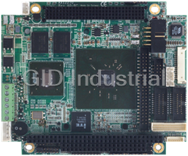


What they say about us
FANTASTIC RESOURCE
One of our top priorities is maintaining our business with precision, and we are constantly looking for affiliates that can help us achieve our goal. With the aid of GID Industrial, our obsolete product management has never been more efficient. They have been a great resource to our company, and have quickly become a go-to supplier on our list!
Bucher Emhart Glass
EXCELLENT SERVICE
With our strict fundamentals and high expectations, we were surprised when we came across GID Industrial and their competitive pricing. When we approached them with our issue, they were incredibly confident in being able to provide us with a seamless solution at the best price for us. GID Industrial quickly understood our needs and provided us with excellent service, as well as fully tested product to ensure what we received would be the right fit for our company.
Fuji
HARD TO FIND A BETTER PROVIDER
Our company provides services to aid in the manufacture of technological products, such as semiconductors and flat panel displays, and often searching for distributors of obsolete product we require can waste time and money. Finding GID Industrial proved to be a great asset to our company, with cost effective solutions and superior knowledge on all of their materials, it’d be hard to find a better provider of obsolete or hard to find products.
Applied Materials
CONSISTENTLY DELIVERS QUALITY SOLUTIONS
Over the years, the equipment used in our company becomes discontinued, but they’re still of great use to us and our customers. Once these products are no longer available through the manufacturer, finding a reliable, quick supplier is a necessity, and luckily for us, GID Industrial has provided the most trustworthy, quality solutions to our obsolete component needs.
Nidec Vamco
TERRIFIC RESOURCE
This company has been a terrific help to us (I work for Trican Well Service) in sourcing the Micron Ram Memory we needed for our Siemens computers. Great service! And great pricing! I know when the product is shipping and when it will arrive, all the way through the ordering process.
Trican Well Service
GO TO SOURCE
When I can't find an obsolete part, I first call GID and they'll come up with my parts every time. Great customer service and follow up as well. Scott emails me from time to time to touch base and see if we're having trouble finding something.....which is often with our 25 yr old equipment.
ConAgra Foods