

 Manufacturers
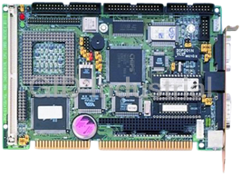
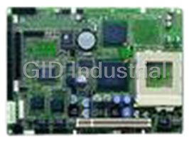
ADVANTECH PCI-6882F-00A1

Description
PCI IntelPentium4/Celeron D/CeleronHalf-sized SBC with VGA/LVDS/LAN/USB2.0/TV-out/ SSD/SATA, PCI Socket 478 Slot PC withLAN/VGA/LVDS/USB/TV-out/SATA
Part Number
PCI-6882F-00A1
Price
Request Quote
Manufacturer
ADVANTECH
Lead Time
Request Quote
Category
Single Board Computers
Specifications
System Chipset
Intel ICH4
Intel 852GME + ICH4
Form Factor
Half-Size PCI
2nd Cache Memory
512 KB on Pentium 4, 256 KB on Celeron D, 128 KB on Celeron
Audio
Supports AC97 Audio with optional PCM-231A-00A1
Battery
Lithium 3 V/196 mAH
BIOS
AWARD 4 Mbit Flash BIOS
Built-in Boot ROM
82541PI, with 82551QM can have this function by optional
CPU
Embedded Intel Pentium 4 processor, up to 3.06 GHz; Celeron D/Celeron process, up to 2.8 GHz
Dimension (L x W)
185 x 122 mm (7.3" x 4.8")
Display Chipset
Intel 852GME chip integrated
Dual Independent Display
CRT + LVDS, LVDS + TV-out, CRT + TV-out, LVDS + LVDS (operate under Windows, Linux)
Ethernet Chipset
Intel 82541PI (Gigabit), Intel 82551ER/82551QM (optional)
Expansion Interface
32-bit PCI slot
GPIO
8-bit general purpose input/output (optional)
I/O Expansion
TV-out, PCI
I/O Interface
2 x IDE, 1 x FDD, 1 x K/B, 1 x Mouse, 2 x SATA, 1 x RS-232/422/485, 3 x RS-232, 1 x LPT
Interface
1 x RJ-45
IrDA
115 kbps, IrDA 1.1 compliant
LCD Interface
2 Channel LVDS (36-bit)
LVDS Interface
Hirose connector supports dual channel LVDS panel
Memory Size
Optimized Shared Memory Architecture, supports up to 64 MB frame buffer using system memory
Operating Humidity
0% ~ 90% relative humidity, non-condensing
Operating Temperature
0 ~ 60°C (32 ~ 140°F)
Power Consumption
Max:7.8 A @ +12 V, 2.4 A @ +5V (w/Pentium 4 3.06 GHz + 1 GB); Typical:2.3 A @ +12 V, 2.3 A @ +5 V (w/Pentium 4 3.06 GHz + 1 GB)
Power Management
APM 1.2, ACPI 2.0 supported
Power Supply Voltage
+5 V, +5 V STB and +12 V
Processor
Intel Pentium 4
Resolution
CRT Mode:up to 1920 x 1440 @ 60 Hz; LVDS Mode:up to 1280 x 1024 @ 36bpp, up to UXGA panel resolution with frequency range from 25 MHz to 112 MHz
Speed
10/100Base-T, 10/100/1000Base-T
SSD
Supports CompactFlash Card Type I/II
Standard
IEEE 802.3 z/ab (1000Base-T) or IEEE 802.3u (100 Base-T) protocol compatible
System Memory
2 x 200 pin DDR SODIMM x 2, support non-ECC DDR up to 2 GB
TV-Out
Supports NTSC and PAL video standard, supports composite, s-video or AV output, graphic resolution up to 1024 x 768 pixels (optional)
USB
4 x USB ports, USB 2.0 compliant
Watch Dog Timer
0 ~ 255 sec., System reset
Weight
0.27 kg (weight of total package)
Features
- Embedded Intel Pentium 4/Celeron D/Celeron Processor
- Supports 2 x SATA ports
- Supports 200 MHz, 266 MHz and 333 MHz DDR SDRAM
- Supports 4 x USB 2.0 ports
- Supports 400/533 MHz Front Side Bus
- Supports up to 1000Base-T Ethernet on board
- Supports up to 2 Channel 36 bits LVDS for LCD
Datasheet

Extracted Text
PCI-6882
PCI Intel® Pentium® 4/Celeron®
D/Celeron® Half-sized SBC with
VGA/LVDS/LAN/USB2.0/TV-out/
SSD/SATA
User Manual
Copyright
This document is copyrighted, © 2006. All rights are reserved. The origi-
nal manufacturer reserves the right to make improvements to the products
described in this manual at any time without notice.
No part of this manual may be reproduced, copied, translated or transmit-
ted in any form or by any means without the prior written permission of
the original manufacturer. Information provided in this manual is
intended to be accurate and reliable. However, the original manufacturer
assumes no responsibility for its use, nor for any infringements upon the
rights of third parties that may result from such use.
Acknowledgements
Award is a trademark of Award Software International, Inc.
VIA is a trademark of VIA Technologies, Inc.
IBM, PC/AT, PS/2 and VGA are trademarks of International Business
Machines Corporation.
Intel and Pentium are trademarks of Intel Corporation.
Microsoft Windows® is a registered trademark of Microsoft Corp.
RTL is a trademark of Realtek Semi-Conductor Co., Ltd.
ESS is a trademark of ESS Technology, Inc.
UMC is a trademark of United Microelectronics Corporation.
SMI is a trademark of Silicon Motion, Inc.
Creative is a trademark of Creative Technology LTD.
All other product names or trademarks are properties of their respective
owners.
For more information on this and other Advantech products, please visit
our websites at: http://www.advantech.com
http://www.advantech.com/eplatform
For technical support and service, please visit our support website at:
http://www.advantech.com/support
This manual is for the PCI-6882.
Part No.200K688210
1st Edition
Feb. 2006
PCI-6882 User Manual ii
Packing List
Before you begin installing your card, please make sure that the following
materials have been shipped:
• 1 PCI-6882 Series Half-sized SBC
• 1 Startup manual
• 1 Utility disk/CD driver
• 1 Y cable for PS/2 Keyboard, PS/2 Mouse p/n: 1700060202
• 1 EIDE (HDD) cable p/n: 1701400452
• 1 FDD cable (600mm) p/n: 1701340603
• 1 Printer port cable p/n: 1700260250
• 1 Power cable p/n: 1700000265
• Mini Jumper p/n: 1653302122
If any of these items are missing or damaged, contact your distributor or
sales representative immediately.
Model No. List Description
PCI-6882F-00A1 PCI Socket 478 Slot PC
w/LAN/VGA/LVDS/USB/TV-out/SATA
PCI-6882FG-00A1 Same as PCI-6882F-00A1 but with
Giga bit Ethernet
PCI-6882L-00A1 Same as PCI-6882F-00A1, without
SATA
iii
Additional Information and Assistance
Visit the Advantech web site at www.advantech.com where you can find
the latest information about the product.
Step 1. Contact your distributor, sales representative, or Advantech's cus-
tomer service center for technical support if you need additional
assistance. Please have the following information ready before
you call:
• Product name and serial number
• Description of your peripheral attachments
• Description of your software (operating system, version, application
software, etc.)
• A complete description of the problem
• The exact wording of any error messages
PCI-6882 User Manual iv
This device complies with the requirements in
part 15 of the FCC rules: Operation is subject to
FCC
the following two conditions:
1.This device may not cause harmful interfer-
ence, and
2. This device must accept any interference
received, including interference that may cause
undesired operation
This equipment has been tested and found to
comply with the limits for a Class A digital device,
pursuant to Part 15 of the FCC Rules. These lim-
its are designed to provide reasonable protection
against harmful interference when the equipment
is operated in a commercial environment. This
equipment generates, uses, and can radiate
radio frequency energy and, if not installed and
used in accordance with the instruction manual,
may cause harmful interference to radio commu-
nications. Operation of this device in a residential
area is likely to cause harmful interference in
which case the user will be required to correct
the interference at his/her own expense. The
user is advised that any equipment changes or
modifications not expressly approved by the
party responsible for compliance would void the
compliance to FCC regulations and therefore,
the user's authority to operate the equipment.
Caution!
There is a danger of a new battery exploding if it
is incorrectly installed. Do not attempt to
recharge, force open, or heat the battery.
Replace the battery only with the same or equiv-
Achtung!
alent type recommended by the manufacturer.
Discard used batteries according to the manufac-
turer’s instructions.
v
PCI-6882 User Manual vi
Contents
Chapter 1 General Information ........................................2
1.1 Introduction ....................................................................... 2
1.2 Features ............................................................................. 2
1.3 Specifications .................................................................... 3
1.3.1 Standard SBC Functions................................................. 3
1.3.2 Display Interface............................................................. 4
1.3.3 TV-out (optional)............................................................ 4
1.3.4 Solid State Disk .............................................................. 4
1.3.5 Ethernet Interface............................................................ 4
1.3.6 Mechanical and Environmental ...................................... 4
1.4 Board layout: dimensions.............................................5
Figure 1.1:Board layout: dimensions (component side). 5
Figure 1.2:Board layout: dimensions (solder side)......... 5
Chapter 2 Installation ........................................................8
2.1 Jumpers.............................................................................. 8
Table 2.1:Jumpers........................................................... 8
2.2 Connectors......................................................................... 9
Table 2.2:Connectors...................................................... 9
2.3 Locating Connectors ...................................................... 10
Figure 2.1:Jumper & Connector Locations (component
side)10
Figure 2.2:Connectors (solder side).............................. 10
2.4 Setting Jumpers ............................................................... 11
2.5 COM2 RS-232/422/485 Select (J2) ................................ 12
Table 2.3:COM2 RS-232/422/485 Select..................... 12
2.6 Clear CMOS (J1)............................................................. 12
Table 2.4: Clear CMOS (J1)....................................... 12
2.7 LCD voltage setting (J3) ................................................. 13
Table 2.5:LCD voltage setting (J3)............................... 13
2.8 SMBus Connector (J4).................................................... 13
Table 2.6:SMBus Connector (J4) ................................. 13
2.9 CPU FSB select Connector (JP1)................................13
Table 2.7:CPU FSB select Connector (JP1) ................. 13
2.10 PCI VIO setting Connector (JP2)................................13
Table 2.8:PCI VIO setting Connector (JP2) ................. 13
2.11 Installing SODIMMs.................................................14
2.12 ATX power control Connector (CN21) .......................... 14
2.13 Printer port Connector (CN5).......................................... 14
2.14 CompactFlash Card Socket ............................................. 15
2.14.1 CompactFlash (CN23) .................................................. 15
vii
2.15 Floppy drive Connector (CN2) ....................................... 15
2.15.1 Connecting the floppy drive ......................................... 15
2.16 IDE Connector (CN3,CN4)............................................. 16
2.16.1 Connecting the hard drive............................................. 16
2.17 LCD/LVDS interface Connections ................................. 17
2.17.1 LVDS Connector (CN16) ............................................. 17
2.17.2 LCD Backlight Connector (CN22)............................... 17
2.18 USB Connectors (CN7, CN8) ......................................... 17
2.19 Ethernet configuration..................................................... 17
2.19.1 LAN Connector (CN12) ............................................... 18
2.19.2 Network boot ................................................................ 18
2.20 Front Panel Connector (CN1) ......................................... 18
2.20.1 Reset (Pin7&Pin8) ........................................................ 18
2.20.2 HDD LED (Pin1&Pin2)................................................ 18
2.20.3 Power LED (Pin 3 & Pin 4).......................................... 18
2.20.4 Suspend LED (Pin 5 & Pin 6)....................................... 18
2.20.5 Power Button (Pin 9 & Pin10)...................................... 18
2.21 COM port Connector (CN13,CN14,CN15) .................... 19
2.22 PS/2, KB/Mouse Connector (CN20)............................... 19
2.23 AC'97 interface Connector (CN11)................................. 19
2.24 DI/O Connector (CN9).................................................... 19
2.25 SATA Connector (SA1, SA2)......................................... 20
Chapter 3 Software Configuration .................................22
3.1 Introduction ..................................................................... 22
3.2 VGA display firmware configuration ............................. 22
Figure 3.1:VGA setup screen........................................ 23
3.3 Connectors to Standard LCDs......................................... 24
3.3.1 AU M170EG01 (1280 x1024 LVDS LCD).................. 24
Table 3.1:Connections to LCD/Flat Panel (CN15)....... 24
Chapter 4 Award BIOS Setup.........................................26
4.1 System test and initialization........................................... 26
4.1.1 System configuration verification................................. 26
4.2 Award BIOS setup .......................................................... 27
4.2.1 Entering setup ............................................................... 27
Figure 4.1:BIOS setup program initial screen .............. 27
4.2.2 Standard CMOS Features setup.................................... 28
Figure 4.2:Standard CMOS Features setup .................. 28
4.2.3 Advanced BIOS Features setup .................................... 29
Figure 4.3:Advanced BIOS Features setup................... 29
4.2.4 Advanced Chipset Features setup................................. 30
Figure 4.4:Advanced Chipset Features setup ............... 30
4.2.5 Integrated Peripherals ................................................... 31
Figure 4.5:Integrated Peripherals.................................. 31
PCI-6882 User Manual viii
4.2.6 Power Management Setup ............................................ 32
Figure 4.6:Power Management Setup........................... 32
4.2.7 PnP/PCI Configurations................................................ 33
Figure 4.7:PnP/PCI Configurations .............................. 33
4.2.8 PC Health Status ........................................................... 34
Figure 4.8:PC Health Status.......................................... 34
4.2.9 Frequency/Voltage Control........................................... 35
Figure 4.9:Frequency/Voltage Control......................... 35
4.2.10 Load Optimized Defaults.............................................. 36
Figure 4.10:Load BIOS defaults screen........................ 36
4.2.11 Set Password................................................................. 36
Figure 4.11:Set password.............................................. 37
4.2.12 Save & Exit Setup......................................................... 38
Figure 4.12:Save to CMOS and EXIT.......................... 38
4.2.13 Exit Without Saving...............................................39
Figure 4.13:Quit without saving ................................... 39
Chapter 5 PCI SVGA Setup ............................................42
5.1 Introduction ..................................................................... 42
5.1.1 Chipset .......................................................................... 42
5.1.2 Display memory............................................................ 42
5.1.3 Display types................................................................. 42
5.2 Installation of the SVGA Driver ..................................... 43
5.2.1 Installation for Windows 2000/XP ............................... 43
5.3 Further Information......................................................... 46
Chapter 6 PCI Bus Ethernet Interface...........................48
6.1 Introduction ..................................................................... 48
6.2 Installation of Ethernet driver ......................................... 48
6.2.1 Installation for Windows XP ........................................ 49
Chapter 7 Audio Setup.....................................................54
7.1 Introduction ..................................................................... 54
7.2 Driver installation............................................................ 54
7.2.1 Before you begin.......................................................... 54
7.2.2 Windows XP driver ..................................................... 54
Appendix A Programming DI/O & Watchdog Timer......58
A.1 Supported DI/O Register................................................. 58
A.1.1 DI/O Registers .............................................................. 58
A.1.2 DI/O Example program-1 ............................................. 59
A.2 Watchdog programming................................................. 59
Appendix B Pin Assignments ............................................62
B.1 Front Panel Connector (CN1) ......................................... 62
Table B.1:Front Panel Connector (CN1) ...................... 62
B.2 Floppy ................................................. Connector (CN2)63
ix
Table B.2:Floppy Connector (CN2) ............................. 63
B.3 Secondary IDE Connector (CN3) ................................... 64
Table B.3:Secondary IDE Connector (CN3) ................ 64
B.4 Primary IDE Connector (CN4)...................................65
Table B.4:Primary IDE Connector (CN4) .................... 65
B.5 Printer Connector (CN5) ................................................. 66
Table B.5:Printer Connector (CN5).............................. 66
B.6 +12V Connector (CN6).............................................67
Table B.6:+12V Connector (CN6) ............................... 67
B.7 USB port 0, 1(CN7) ........................................................ 67
Table B.7:USB port 0, 1 (CN7) .................................... 67
B.8 USB port 2, 3 (CN8) ....................................................... 67
Table B.8:USB port 2, 3 (CN8) .................................... 67
B.9 DI/O Connector (CN9).................................................... 68
Table B.9:DI/O Connector (CN9) ................................ 68
B.10 VGA D-SUB Connector (CN10) .................................... 69
Table B.10:VGA D-SUB Connector (CN10)............... 69
B.11 AC’97 Interface Connector (CN11)............................69
Table B.11: AC’97 Interface Connector (CN11).......... 69
B.12 LAN Connector (CN12).................................................. 70
Table B.12: LAN Connector (CN12) ........................... 70
B.13 COM2 (RS-232/422/485) (CN13) .................................. 70
Table B.13:COM2 connector (CN13) .......................... 70
B.14 COM 3, 4 Connector (CN14).....................................71
Table B.14:COM 3, 4 Connector (CN14)..................... 71
B.15 COM1 Connector (CN15)............................................... 71
Table B.15:COM1 Connector (CN15).......................... 71
B.16 LVDS Connector (CN16)................................................ 72
Table B.16:LVDS Connector (CN16) .......................... 72
B.17 IrDA Connector (CN17)............................................72
Table B.17:IrDA Connector (CN17) ............................ 72
B.18 TV-out Connector (CN18).........................................73
Table B.18:TV-out Connector (CN18)......................... 73
B.19 AT Keyboard Connector (CN19)................................73
Table B.19:AT Keyboard Connector (CN19)............... 73
B.20 ATX power Connector (CN21)....................................... 74
Table B.20:ATX power Connector (CN21) ................. 74
B.21 LCD backlight Connector (CN22) .................................. 74
Table B.21:LCD backlight Connector (CN22)............. 74
B.22 CompactFlash Connector (CN23)................................... 75
Table B.22:CompactFlash Connector (CN23).............. 75
B.23 FAN Connector (FAN1)............................................76
Table B.23:FAN Connector (FAN1) ............................ 76
B.24 Serial ATA (SA1,SA2) ................................................... 76
PCI-6882 User Manual x
Table B.24:Serial ATA (SA1, SA2) ............................. 76
Appendix C System Assignments ......................................80
C.1 System I/O Ports.............................................................. 80
Table C.1:System I/O ports .......................................... 80
C.2 1st MB memory map....................................................... 81
Table C.2:1st MB memory map ................................... 81
C.3 DMA channel assignments.............................................. 81
Table C.3:DMA channel assignments .......................... 81
C.4 Interrupt assignments ...................................................... 82
Table C.4:Interrupt assignments................................... 82
xi
PCI-6882 User Manual xii
1
General Information
This chapter gives background
information on the PCI-6882.
Sections include:
• Introduction
• Features
• Specifications
• Board layout and dimensions
1 Chapter 1 General Information
CHAPTER
Chapter 1 General Information
1.1 Introduction
The PCI-6882 series is a half-sized PCI bus CPU card designed with
powerful Intel® Pentium® 4, Celeron® D or Celeron processor, with
Intel 852GME and ICH4 chipset, which supports Dynamic Video Mem-
ory Technology. For maximum performance, PCI-6882 also supports two
200 PIN DDR SODIMM sockets for non-ECC DDR memory up to 2 GB.
These chipsets are specifically for embedded computing and provide an
optimized onboard integrated graphics solution. Hyper-Threading tech-
nology intelligently focuses system power where the CPU needs it and
automatically regulates power usage to preserve battery life.
Other onboard features include 2 EIDE, 2 SATA, 1 FDD, 4 USB 2.0, 4
COM ports (3 x RS-232 and 1 x RS-232/422/485), PS/2 Keyboard/
mouse, watchdog, and a DI/O interface. The SSD solution supports Type
I/II CompactFlash cards.
PCI-6882 uses the Intel 852GME chipset which supports CRT/LVDS
interface and a 2 channel (36-bit) LVDS LCD panel. PCI-6882 supports
AC’97 audio with the addition of the optional PCM-231A-00A1 audio
module.
The Ethernet interface supports IEEE 802.3u (100Base-T) by Intel
82551ER (82551QM optional), and 1000Base-T by Intel 82541PI (PCI-
6882FG-00A1). PCI-6882 follows standard PCI slot dimensions, this
means it can match with all half-sized chassis and can operate in high
vibration environments.
1.2 Features
• Intel new generation Intel Pentium 4/Celeron D/Celeron Processor
Embedded
• Operation at 0~60° C
• Onboard PCI CRT/LVDS/TV-out display
• Supports 1000Base-T Ethernet on board (PCI-6882FG-00A1)
• Supports 2 SATA
• Supports 4 x USB 2.0 ports
PCI-6882 User Manual 2
• Supports 2 Channel 18 bits LVDS for LCD
• Supports 400/533 MHz Front Side Bus
• Supports 200 MHz, 266 MHz and 333 MHz DDR SDRAM
1.3 Specifications
1.3.1 Standard SBC Functions
• CPU: Intel Pentium 4 processor, up to 3.06 GHz; Celeron D and Cele-
ron processor, up to 2.8 GHz; Supports 400 MHz FSB processors.
• System Chipset: Intel 852GME + ICH4
• BIOS: Award 4 Mbit Flash memory
• System memory: 200 pin DDR SODIMM x 2, supports non-ECC DDR
up to 2 GB
• 2nd cache memory: 512 KB on Pentium® 4 processor, 256 KB on Cel-
eron® D processor, 128 KB on Celeron® processor
• Enhanced IDE Interface: Supports two enhanced IDE channels. Pri-
mary channel supports up to ATA-100 mode; Secondary channel
only supports up to ATA-33. The CFC card occupies the secondary
master channel
• COM Ports: Four COM ports, COM1, COM3, COM4: RS-232,
COM2: RS-232/422/485
• Printer Port: One printer port, supports SPP/EPP/ECP
• Keyboard/Mouse Connector: One 6-pin socket on bracket for stan-
dard PS/2 Mouse and Keyboard, one 5-pin wafer box connector for
external Keyboard only.
• Power Management: Supports Power Saving Mode including Normal/
Standard/Suspend modes. APM 1.2 compliant. ACPI 1.0b, ACPI
2.0 supported
• FDD interface: Supports up to two FDD devices
• Watchdog Timer: 0~255 Sec., System reset
• Expansion Interface: PCI interface, compatible with PCI Rev 2.2
• USB: 4 USB ports, USB 2.0 compliant
• SATA Connector: Two COMAX C504C connectors, supports data
transfer rate up to 150 MB/s, Software RAID 0, 1 supported
(Depend on Adapter)
• DI/O Interface: 8-bit general purpose input/output (optional)
• SSD: Supports CompactFlash Card Type I/II
• IrDA: 115 kbps, IrDA1.1 compliant
• Audio: Supports AC’97 Audio with optional PCM-231A-00A1
3 Chapter 1 General Information
1.3.2 Display Interface
• Chipset: Intel 852GME chip integrated
• Memory size: Optimized Shared Memory Architecture, supports up to
64 MB frame buffer using system memory
• Display modes:
CRT Modes: 1920 x 1440 @ 60 Hz; 1600 x 1200 @ 85 Hz
LCD Modes: up to 1280 x 1024 @ 36bpp
• LCD Interface: 2 Channel LVDS (2 x 18-bit)
• LVDS Interface: Hirose connector supports dual channel LVDS panel,
up to UXGA panel resolution with frequency range from 25 MHz to
112 MHz
• Dual Display: CRT + LVDS, LVDS + TV-out, CRT + TV-out, LVDS
+ LVDS (under Windows, Linux)
1.3.3 TV-out (optional)
• Chipset: Chrontel CH7009
• Supports NTSC and PAL video standards
• Supports composite, s-video or AV output
• Supports graphic resolutions up to 1024 x 768 pixels
1.3.4 Solid State Disk
• Supports CompactFlash Card I/II
1.3.5 Ethernet Interface
• Chipset: Intel 82541PI (Gigabit), Intel 82551ER/82551QM (optional)
• Connection: Onboard RJ-45 connector
• Interface: IEEE 802.3 z/ab (1000Base-T) or IEEE 802.3u (100Base-T)
protocol compatible
1.3.6 Mechanical and Environmental
• Dimensions (L x W): 185 x 122 mm (7.3” x 4.8”)
• Power supply voltage: +5 V, +5 V STB, +12 V
• Power requirements:
Max:
7.8 A @+12 V, 2.4 A@+5 V (with Pentium4 3.06 GHz + 1 GB);
Typical:
2.3 A @+12 V, 2.3 A @+5 V (with Pentium4 3.06 GHz + 1 GB);
• Operating temperature: 0 ~ 60° C (32 ~ 140° F) operation
• Operating humidity: 0 ~ 90% Relative Humidity, Non condensing
PCI-6882 User Manual 4
1.4 Board layout: dimensions
3.00
185.00
154.33
129.06
70.76 36.13
4.19
4.00 22.50 6.48
6.41
2.80
4.01 4.01
14.29
4.13
24.38
6.41
59.44
4.91
56.26
62.48
24.93
6.08
65.75 76.20
25.35
121.92
58.80
16.19
13.06
7.07
65.66
2.68
30.56
9.91
27.43
20.14
2.89
5.72 11.43
5.08
7.60
36.08
65.75
104.47
Figure 1.1: Board layout: dimensions (component side)
46.35
5.40
20.86
75.72
Figure 1.2: Board layout: dimensions (solder side)
5 Chapter 1 General Information
PCI-6882 User Manual 6
2
Installation
This chapter explains the setup procedures
of PCI-6882 hardware, including instruc-
tions on setting jumpers and connecting
peripherals, switches and indicators. Be
sure to read all safety precautions before
you begin the installation procedure.
7 Chapter 2 Installation
CHAPTER
Chapter 2 Installation
2.1 Jumpers
The PCI-6882 has a number of jumpers that allow you to configure your
system to suit your application. The table below lists the functions of the
various jumpers.
Table 2.1: Jumpers
Label Function
J1 CMOS setting
J2 COM2 RS-232/422/485 setting Connector
J3 LCD voltage setting
J4 SMBus Connector
JP1 CPU FSB setting Connector
JP2 PCI VIO setting Connector
BT1 Battery socket
PCI-6882 User Manual 8
2.2 Connectors
Onboard connectors link the PCI-6882 to external devices such as hard
disk drives, a keyboard, or floppy drives. The table below lists the func-
tion of each of the board’s connectors.
Table 2.2: Connectors
Label Function
CN1 Front Panel Connector
CN2 Floppy Connector
CN3 Secondary IDE Connector
CN4 Primary IDE Connector
CN5 Printer Connector
CN6 +12V Connector
CN7 USB port 0, 1
CN8 USB port 2, 3
CN9 DI/O Connector
CN10 D-SUB VGA Connector
CN11 AC’97 interface Connector
CN12 LAN Connector
CN13 COM2 (RS-232/422/485)
CN14 COM3, COM4 (RS-232)
CN15 COM1 Connector
CN16 LVDS Connector
CN17 IrDA Connector
CN18 TV-out Connector
CN19 AT keyboard Connector
CN20 PS/2 Mouse/Keyboard Connector
CN21 ATX Connector
CN22 LCD Backlight Connector
CN23 CompactFlash Socket
SA1 SATA Connector
SA2 SATA Connector
FAN1 FAN Connector
9 Chapter 2 Installation
2.3 Locating Connectors
CN1 CN2 CN5 CN4 CN3
SA1 CN7
CN6
SA2
FAN1
CN8
CN9
CPU1
CN10
CN11
J1
CN12
CN13
CN15
CN14
J2
CN21
CN20
J4
J3 JP2
CN19 CN22 CN18 CN17 JP1 CN16
Figure 2.1: Jumper & Connector Locations (component side)
CN3
CN23
CN21
Figure 2.2: Connectors (solder side)
PCI-6882 User Manual 10
2.4 Setting Jumpers
You may configure your card to match the needs of your application by
setting jumpers. A jumper is a metal bridge used to close an electric cir-
cuit. It consists of two metal pins and a small metal clip (often protected
by a plastic cover) that slides over the pins to connect them. To close a
jumper, you connect the pins with the clip. To open a jumper, you remove
the clip. Sometimes a jumper will have three pins, labeled 1, 2 and 3. In
this case you would connect either pins 1 and 2, or 2 and 3.
open closed closed 2-3
The jumper settings are schematically depicted in this manual as follows:.
open closed closed 2-3
A pair of needle-nose pliers may be helpful when working with jumpers.
If you have any doubts about the best hardware configuration for your
application, contact your local distributor or sales representative before
you make any changes. Generally, you simply need a standard cable to
make most connections.
11 Chapter 2 Installation
2.5 COM2 RS-232/422/485 Select (J2)
1 2
3 4
5 6
Table 2.3: COM2 RS-232/422/485 Select
1-2 (default) RS-232
3-4 RS-422
5-6 RS-485
Empty
The IR function is available
2.6 Clear CMOS (J1)
Warning! To avoid damaging the computer, always turn
off the power supply before setting “Clear
CMOS.” Before turning on the power supply,
set the jumper back to “3.0 V Battery On.”
This jumper is used to erase CMOS data (including the setting of date,
time and password) and reset system BIOS information.
The procedure for clearing CMOS is:
1. Turn off the system.
2. Short pin 1 and pin 2.
3. Turn on the system. The BIOS is now reset to its default setting
Table 2.4: Clear CMOS (J1)
Clear CMOS
PCI-6882 User Manual 12
2.7 LCD voltage setting (J3)
123 1 23
Table 2.5: LCD voltage setting (J3)
Pin Function
1-2(default) +5 V
2-3 +3.3 V
2.8 SMBus Connector (J4)
Table 2.6: SMBus Connector (J4)
Pin Function
1+5 V
2SM_CLOCK
3SM_DATA
4GND
2.9 CPU FSB select Connector (JP1)
Table 2.7: CPU FSB select Connector (JP1)
Pin Function
1~2 (default) Auto detect
2~3 100 MHz
Empty 133 MHz
2.10 PCI VIO setting Connector (JP2)
Table 2.8: PCI VIO setting Connector (JP2)
Pin Function
1~2 (default) +5 V
2~3 +3.3 V
13 Chapter 2 Installation
2.11 Installing SODIMMs
Notes
The modules can only fit into a socket one way.
The gold pins must point down into the
SODIMM socket.
Follow the below procedure for installing SODIMMs. Please follow these
steps carefully.
1. Make sure that all power supplies to the system are switched off
2. Install the SODIMM card. Install the SODIMM so that its gold pins
point down into the SODIMM socket.
3. Slip the SODIMM into the socket at a 45 degree angle and care-
fully fit the bottom of the card against the connectors.
4. Gently push the SODIMM into a perpendicular position until the
clips on the ends of the SODIMM sockets snap into place.
5. Check to ensure that the SODIMM is correctly seated and all con-
nector contacts touch. The SODIMM should not move around in its
socket.
2.12 ATX power control Connector (CN21)
The PCI-6882 supports ATX power. CN21 supplies main power (PS-ON,
5 VSB), and is a 3 pins power connector, w/Fixed Lock, type: 4200-WS-
A1.
Important
Make sure that the ATX power supply can take
at least a 10 mA load on the 5 V standby lead
(5VSB). If not, you may have difficulty power-
ing on your system.
2.13 Printer port Connector (CN5)
Normally, the printer port is used to connect the card to a printer. The
PCI-6882 includes a multi-mode (ECP/EPP/SPP) printer port accessed
via CN5 and a 26-pin flat-cable connector. You will need an adapter
PCI-6882 User Manual 14
cable if you use a traditional DB-25 connector. The adapter cable has a
26-pin connector on one end, and a DB-25 connector on the other.
The printer port is designated as LPT1, and can be disabled or changed to
LPT2 or LPT3 in the system BIOS setup.
The printer port interrupt channel is designated to be IRQ7.
You can select ECP/EPP DMA channel via BIOS setup.
2.14 CompactFlash Card Socket
The PCI-6882 provides a 50-pin socket for CompactFlash card type I/II.
2.14.1 CompactFlash (CN23)
The CompactFlash card occupies a secondary IDE channel which can be
enabled/disabled via the BIOS settings.
2.15 Floppy drive Connector (CN2)
You can attach up to two floppy drives to the PCI-6882’s onboard con-
troller. You can use any combination of 5.25” (360 KB and 1.2 MB) and/
or 3.5” (720 KB, 1.44 MB, and 2.88 MB) drives.
A 34-pin daisy-chain drive connector cable is required for a dual-drive
system. On one end of the cable is a 34-pin flat-cable connector. On the
other end are two sets of floppy disk drive connectors. Each set consists
of a 34-pin flat-cable connector (usually used for 3.5” drives) and a
printed-circuit board connector (usually used for 5.25” drives).
2.15.1 Connecting the floppy drive
1. Plug the 34-pin flat-cable connector into CN2. Make sure that the
red wire corresponds to pin one on the connector.
2. Attach the appropriate connector on the other end of the cable to
the floppy drive(s). You can use only one connector in the set. The
set on the end (after the twist in the cable) connects to the A: drive.
The set in the middle connects to the B: drive.
3. If you are connecting a 5.25” floppy drive, line up the slot in the
printed circuit board with the blocked-off part of the cable connec-
tor.
If you are connecting a 3.5” floppy drive, you may have trouble determin-
ing which pin is number one. Look for a number printed on the circuit
board indicating pin number one. In addition, the connector on the floppy
drive may have a slot. When the slot is up, pin number one should be on
15 Chapter 2 Installation
the right. Check the documentation that came with the drive for more
information.
If you desire, connect the B: drive to the connectors in the middle of the
cable as described above.
In case you need to make your own cable, you can find the pin assign-
ments for the board’s connector in Appendix B.
2.16 IDE Connector (CN3,CN4)
The PCI-6882 provides two IDE channels to which you can attach up to
four Enhanced Integrated Device Electronics hard disk drives or CD-
ROM to the PCI-6882’s internal controller. The PCI-6882's IDE control-
ler uses a PCI interface. This advanced IDE controller supports faster data
transfer. Primary channel (CN4) supports ATA-100 mode; Secondary
channel (CN3) only supports ATA-33 and PIO mode. The CFC card
occupies the secondary master channel.
2.16.1 Connecting the hard drive
Connecting drives is done in a daisy-chain fashion. It requires one of two
cables (not included in this package), depending on the drive size. 1.8"
and 2.5" drives need a 1 x 44-pin to 2 x 44-pin flat-cable connector. 3.5"
drives use a 1 x 44-pin to 2 x 40-pin connector.
Wire number 1 on the cable is red or blue, and the other wires are gray.
1. Connect one end of the cable to CN3, CN4. Make sure that the red
(or blue) wire corresponds to pin 1 on the connector, which is
labelled on the board (on the right side).
2. Plug the other end of the cable into the Enhanced IDE hard drive,
with pin 1 on the cable corresponding to pin 1 on the hard drive.
(See your hard drive’s documentation for the location of the con-
nector.)
If desired, connect a second drive as described above.
Unlike floppy drives, IDE hard drives can connect to either end of the
cable. If you install two drives, you will need to set one as the master and
one as the slave by using jumpers on the drives. If you install only one
drive, set it as the master.
PCI-6882 User Manual 16
2.17 LCD/LVDS interface Connections
The PCI-6882’s display interface can drive conventional CRT displays
and is capable of driving a wide range of LVDS flat panel displays as
well. The board has two display connectors: one for standard CRT VGA
monitors, and one for LVDS flat panel displays.
2.17.1 LVDS Connector (CN16)
PCI-6882 uses the Intel 852GME to support single or dual-channel
LVDS panels up to UXGA panel resolution with frequency range from
25 MHz to 112 MHz.
The display mode can be 2 channels (2 x 18bit) LVDS LCD panel dis-
plays Users can connect to either an 18, 24, or 36bit LVDS LCD with
CN16.
2.17.2 LCD Backlight Connector (CN22)
The LCD inverter is connected to CN22 via a 5-pin connector to provide
+5 V / +12 V power.
2.18 USB Connectors (CN7, CN8)
The PCI-6882 board provides up to four USB (Universal Serial Bus)
ports. This gives complete Plug and Play, and hot attach/detach for up to
127 external devices. The USB interfaces complies with USB specifica-
tion Rev. 2.0, and are fuse protected.
The USB interface is accessed through the 5 x 2-pin flat-cable connector,
CN7 (USB0, 1), and CN8 (USB2, 3). You will need an adapter cable if
you use a standard USB connector. The adapter cable has a 5 x 2-pin con-
nector on one end and a USB connector on the other.
The USB interfaces can be disabled in the system BIOS setup.
2.19 Ethernet configuration
The PCI-6882 is equipped with a high performance 32-bit PCI-bus Ether-
net interface which is fully compliant with IEEE 802.3u 10/100 Mbps
CSMA/CD standards. It is supported by all major network operating sys-
tems.
The PCI-6882 supports 10/100Base-T or 1000Base-T Ethernet connec-
tions with onboard RJ-45 connectors (CN12). PCI-6882F series supports
10/100Base-T LAN, PCI-6882FG series supports 1000Base-T LAN.
17 Chapter 2 Installation
2.19.1 LAN Connector (CN12)
10/100 or 1000 Base-T connects to the PCI-6882 via a cable to a standard
RJ-45 connector.
2.19.2 Network boot
The Network Boot feature can be utilized by incorporating the Boot
ROM image files for the appropriate network operating system. The Boot
ROM BIOS files are included in the system BIOS, which is on the utility
CD disc. Boot ROM function supported by 82541PI and 82551QM
(optional), 82551ER can not support this function.
2.20 Front Panel Connector (CN1)
Next is to install external switches to monitor and control PCI-6882.
These features are optional: install them only if necessary. CN1 is an 2 x
5 pin header, 180 degree, male.It provides connections for reset and
power & hard disk indicator.
2.20.1 Reset (Pin7&Pin8)
If a reset switch is installed, it should be an open single pole switch.
Momentarily pressing the switch will activate a reset. The switch should
be rated for 10 mA, 5 V.
2.20.2 HDD LED (Pin1&Pin2)
The HDD LED indicator for hard disk access is an active low signal (24
mA sink rate).
Pin 1 & Pin 2
The HDD LED indicator lights up when the HDD is operating.
2.20.3 Power LED (Pin 3 & Pin 4)
Pin 3 & Pin 4
The Power LED indicator lights up when the power is on.
2.20.4 Suspend LED (Pin 5 & Pin 6)
Pin 5 & Pin 6
The Suspend LED indicator lights up when the computer is in suspend
mode.
2.20.5 Power Button (Pin 9 & Pin10)
The PCI-6882 provides an ATX power input connector. When connected
with Pin 9 & Pin 10, it enables power On/Off from the chassis.
PCI-6882 User Manual 18
2.21 COM port Connector (CN13,CN14,CN15)
The PCI-6882 provides four COM ports (COM1, COM3, COM4: RS-232
and COM2: RS-232/422/485). CN15 supports COM1, CN13 supports
COM2, CN14 supports COM3, COM4. and J2 is for COM2 RS-232/422/
485 selection. It provides connections for serial devices (a mouse, etc.) or
a communication network. You can find the pin assignments for the
COM port connector in Appendix B.
2.22 PS/2, KB/Mouse Connector (CN20)
The PCI-6882 board provides a keyboard connector that supports both a
keyboard and a PS/2 style mouse. In most cases, especially in embedded
applications, a keyboard is not used. If the keyboard is not present, the
standard PC/AT BIOS will report an error or fail during power-on self-
test (POST) after a reset. The PCI-6882’s BIOS standard setup menu
allows you to select "All, But Keyboard" under the "Halt On" selection.
This allows no-keyboard operation in embedded system applications,
without the system halting under POST.
2.23 AC'97 interface Connector (CN11)
PCI-6882 can support separate independent PCI functions for Audio and
Modem, which is compliant to AC'97 2.2 standard.
The AC'97 interface is a 5 x 2 pin box header. PCI-6882 can support
Audio with the addition of optional PCM-231A-00A1. Detailed pin
assignment refer to Appendix B.
2.24 DI/O Connector (CN9)
The PCI-6882 supports DI/O interface by CN9, which is a 5 x 2 dual line
pin header, supplying 8-bit general purpose input or output ports.
Generally, Digital Input and Output are signals to control external devices
that need an On/Off circuit or TTL devices. For detailed signal assign-
ment refer to Appendix A.
19 Chapter 2 Installation
2.25 SATA Connector (SA1, SA2)
PCI-6882 can support Serial ATA by two COMAX C504C connectors
(SA1, SA2), with data transfer rates up to 150 Mb/s, enabling very fast
data and file transfer, and independent DMA operation on two ports. It
also supports alternate Device ID and RAID Class Code option for sup-
port of Soft RAID.
PCI-6882 User Manual 20
3
Software Configuration
This chapter details the software con-
figuration information. It shows you
how to configure the card to match
your application requirements. Award
System BIOS will be covered in
Chapter 4.
Sections include:
• Introduction
• VGA display software configuration
• Connectors to Standard LCDs
CHAPTER
Chapter 3 Software Configuration
3.1 Introduction
The system BIOS and custom drivers are located in a 512 KB, 32-pin
(JEDEC spec.) Flash ROM device, designated U10. A single Flash chip
holds the system BIOS, VGA BIOS, and network Boot ROM image. The
display can be configured via software. This method minimizes the num-
ber of chips and eases configuration. You can change the display BIOS
simply by reprogramming the Flash chip.
NOTE: Due to Intel not supporting Win98 and Windows
ME, it is not recommended to install Win98,
Windows ME drivers on PCI-6882.
3.2 VGA display firmware configuration
The onboard VGA interface supports a wide range of popular LCD, flat
panel displays and traditional analog CRT monitors. The 852GME chip
with optimized Shared Memory Architecture, supports up to 64 MB
frame buffer using system memory to provide LVDS mode up to 1280 x
1024 @ 36bpp, the interface can drive CRT displays with resolutions up
to 1920 x 1440 @ 60 Hz and 1600 x 1200 @ 85 Hz.
The VGA interface is configured completely via the software utility, so
you do not have to set any jumpers. Configure the VGA display as fol-
lows:
1. Apply power to the board with a color TFT display attached. This
is the default setting for this board. Ensure that the AWD-
FLASH.EXE and *.BIN files are located in the working drive.
NOTE: Ensure that you do not run AWDFLASH.EXE
while your system is operating in EMM386
mode.
PCI-6882 User Manual 22
2. At the prompt, type AWDFLASH.EXE and press immediately. This will allow you
to enter Setup.
Figure 4.1: BIOS setup program initial screen
27
4.2.2 Standard CMOS Features setup
When you choose the Standard CMOS Features option from the Initial
Setup Screen menu, the screen shown below is displayed. This standard
Setup Menu allows users to configure system components such as date,
time, hard disk drive, floppy drive and display. Once a field is high-
lighted, on-line help information is displayed in the right top of the Menu
screen.
Figure 4.2: Standard CMOS Features setup
PCI-6882 User Manual 28
4.2.3 Advanced BIOS Features setup
By choosing the Advanced BIOS Features Setup option from the Initial
Setup Screen menu, the screen below is displayed. This sample screen
contains the manufacturer’s default values for the PCI-6882 Series.
Figure 4.3: Advanced BIOS Features setup
29
4.2.4 Advanced Chipset Features setup
By choosing the Advanced Chipset Features option from the Initial Setup
Screen menu, the screen below is displayed. This sample screen contains
the manufacturer’s default values for the PCI-6882 Series.
Figure 4.4: Advanced Chipset Features setup
PCI-6882 User Manual 30
4.2.5 Integrated Peripherals
Choosing the Integrated Peripherals option from the Initial Setup Screen
menu should produce the screen below. Here we see the manufacturer’s
default values for the PCI-6882 Series.
Figure 4.5: Integrated Peripherals
31
4.2.6 Power Management Setup
By choosing the Power Management Setup option from the Initial Setup
Screen menu, the screen below is displayed. This sample screen contains
the manufacturer’s default values for the PCI-6882 Series.
Figure 4.6: Power Management Setup
PCI-6882 User Manual 32
4.2.7 PnP/PCI Configurations
By choosing the PnP/PCI Configurations option from the Initial Setup
Screen menu, the screen below is displayed. This sample screen contains
the manufacturer’s default values for the PCI-6882 Series.
Figure 4.7: PnP/PCI Configurations
33
4.2.8 PC Health Status
The PC Health Status option displays information such as CPU and moth-
erboard temperatures, fan speeds, and core voltage.
Figure 4.8: PC Health Status
PCI-6882 User Manual 34
4.2.9 Frequency/Voltage Control
By choosing the Frequency/Voltage Control option from the Initial Setup
Screen menu, the screen below is displayed. This sample screen contains
the manufacturer’s default values for the PCI-6882
Figure 4.9: Frequency/Voltage Control
Caution Incorrect settings in Frequency/Voltage Control
may damage the system CPU, video adapter,
or other hardware.
35
4.2.10 Load Optimized Defaults
Load Optimized Defaults loads the default system values directly from
ROM. If the stored record created by the Setup program should ever
become corrupted (and therefore unusable), these defaults will load auto-
matically when you turn the PCI-6882 Series system on.
Figure 4.10: Load BIOS defaults screen
4.2.11 Set Password
Note To enable this feature, you should first go to the
Advanced BIOS Features menu, choose the
Security Option, and select either Setup or
System, depending on which aspect you want
password protected. Setup requires a pass-
word only to enter Setup. System requires the
password either to enter Setup or to boot the
system.
A password may be at most 8 characters long.
PCI-6882 User Manual 36
To Establish Password
1. Choose the Set Password option from the CMOS Setup Utility
main menu and press
Frequently asked questions
How does Industrial Trading differ from its competitors?

Is there a warranty for the PCI-6882F-00A1?
Which carrier will Industrial Trading use to ship my parts?
Can I buy parts from Industrial Trading if I am outside the USA?
Which payment methods does Industrial Trading accept?
Why buy from GID?

Quality
We are industry veterans who take pride in our work

Protection
Avoid the dangers of risky trading in the gray market

Access
Our network of suppliers is ready and at your disposal

Savings
Maintain legacy systems to prevent costly downtime

Speed
Time is of the essence, and we are respectful of yours
Related Products
ISA 486 Slot-PC SBC, with VGA/LCD/LAN/DOC and PC/104
Advantech 1906618403 CPU Board. VGA/LAN/HISA-(FSB 533) rev A2 Processor System CPU Intel Pentium 4, ...
Advantech 1906618608 CPU Boards. Socket 478 | Pentium 4/Celeron Processor | VGA/Dual Gigabit LAN | H...
Advantech 1906957112 CPU Board
Socket 370 SBC with 3 LAN, and VGA/LCD
LGA 775 Core 2 Duo/Pentium D/ Pentium 4/Celeron D Processor-based ATX with DDR2/PCIe/Dual GbE LAN
Request a Quote

The quote request has been received
Close

Facing challenges or have inquiries? Feel free to contact us!
Call Us +1-469-283-2440
What they say about us
FANTASTIC RESOURCE
One of our top priorities is maintaining our business with precision, and we are constantly looking for affiliates that can help us achieve our goal. With the aid of GID Industrial, our obsolete product management has never been more efficient. They have been a great resource to our company, and have quickly become a go-to supplier on our list!
Bucher Emhart Glass
EXCELLENT SERVICE
With our strict fundamentals and high expectations, we were surprised when we came across GID Industrial and their competitive pricing. When we approached them with our issue, they were incredibly confident in being able to provide us with a seamless solution at the best price for us. GID Industrial quickly understood our needs and provided us with excellent service, as well as fully tested product to ensure what we received would be the right fit for our company.
Fuji
HARD TO FIND A BETTER PROVIDER
Our company provides services to aid in the manufacture of technological products, such as semiconductors and flat panel displays, and often searching for distributors of obsolete product we require can waste time and money. Finding GID Industrial proved to be a great asset to our company, with cost effective solutions and superior knowledge on all of their materials, it’d be hard to find a better provider of obsolete or hard to find products.
Applied Materials
CONSISTENTLY DELIVERS QUALITY SOLUTIONS
Over the years, the equipment used in our company becomes discontinued, but they’re still of great use to us and our customers. Once these products are no longer available through the manufacturer, finding a reliable, quick supplier is a necessity, and luckily for us, GID Industrial has provided the most trustworthy, quality solutions to our obsolete component needs.
Nidec Vamco
TERRIFIC RESOURCE
This company has been a terrific help to us (I work for Trican Well Service) in sourcing the Micron Ram Memory we needed for our Siemens computers. Great service! And great pricing! I know when the product is shipping and when it will arrive, all the way through the ordering process.
Trican Well Service
GO TO SOURCE
When I can't find an obsolete part, I first call GID and they'll come up with my parts every time. Great customer service and follow up as well. Scott emails me from time to time to touch base and see if we're having trouble finding something.....which is often with our 25 yr old equipment.
ConAgra Foods