

 Manufacturers
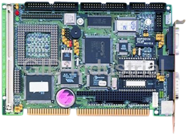
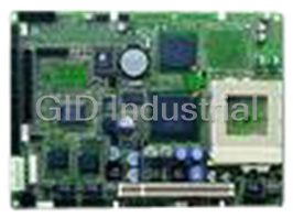
ADVANTECH PCA-6752F

Description
ISA Super 7 Slot SBC, with VGA/LAN/DOC
Part Number
PCA-6752F
Price
Request Quote
Manufacturer
ADVANTECH
Lead Time
Request Quote
Category
Single Board Computers
Specifications
System Chipset
VIA VT82C686
VIA MVP4 (VT82C686 + VT8501)
Ethernet Chipset
Realtek RTL8139C
Video Chipset
PCA-6752F
Form Factor
Half-Size ISA
General
Resolution 800 x 600 @ 24 bpp(CRT)1024 x 768 @ 24 bpp (CRT)
2nd Cache Memory
512KB PBSRAM (66/100 MHz)
Battery
Lithium 3 V /196 mAH
BIOS
AWARD 256KB Flash BIOS
CPU
Socket 7 Intel P54C/P55C, AMD K5/K6/K6-2/K6-3 up to 550 MHz
Dimensions (LxW)
185 x 122 mm (7.3” x 4.8”)
Display
Chipset VIA MVP4 built-in VGA controller, AGP 2X
Ethernet
Chipset RTL8139C
Expansion Interface
16-bit ISA
I/O
MIO 1 x EIDE (UltraDMA66), 1 x FDD, 1 x K/B, 1 x Mouse, 1 x RS-232/422/485, 1 x RS-232, 1 x LPT
Power Management
APM 1.1
SSD
DiskOnChip
System Memory
SDRAM DIMM x 1, Max. 128 MB
Watchdog Timer
1 - 62 Sec, System reset or IRQ11
Features
- 66/100 MHz FSB
- Core Logic integrated 2X AGP 2.0 compliant graphics feature
- Support Super 7 architecture
- Supports full DVD 1.0, VCD 2.0 and CD-Karaoke
- Supports wake-up on LAN, modem
Datasheet

Extracted Text
PCA-6752 Series
Super7™ Half-size card PC with
VGA/LCD and Ethernet
Copyright Notice
This document is copyrighted, 2000. All rights are reserved. The
original manufacturer reserves the right to make improvements to the
products described in this manual at any time without notice.
No part of this manual may be reproduced, copied, translated or
transmitted in any form or by any means without the prior written
permission of the original manufacturer. Information provided in this
manual is intended to be accurate and reliable. However, the original
manufacturer assumes no responsibility for its use, nor for any
infringements upon the rights of third parties which may result from
its use.
Acknowledgements
Award is a trademark of Award Software International, Inc.
IBM, PC/AT, PS/2 and VGA are trademarks of International Business
Machines Corporation.
Intel and Pentium are trademarks of Intel Corporation.
®
Microsoft Windows is a registered trademark of Microsoft Corp.
UMC is a trademark of United Microelectronics Corporation.
All other product names or trademarks are properties of their
respective owners.
For more information on this and other Advantech products please
visit our website at: http://www.advantech.com
http://www.advantech.com/epc
For technical support and service for please visit our support website
at: http://www.advantech.com/support
This manual is for the PCA-6752F/6752N
Part No. 2006675200 1st Edition
Printed in Taiwan May 2000
Packing List
Before installing your board, ensure that the following materials have
been received:
1 PCA-6752 all-in-one single board computer
1 Ultra ATA (HDD) cable (457 mm) p/n: 1701400453
1 floppy disk drive interface cable (700 mm) p/n: 1701340700
1 COM port/Parallel port cable p/n: 1701260303
1 Y cable for AT-keyboard, PS/2 mouse (190 mm)
p/n: 1700060201
1 ATX/AT power cable p/n: 1700040052
1 startup manual
CD-ROM or disks for utility, drivers, and manual (in PDF format)
Warranty certificate
Optional devices:
IrdA adapter: p/n: 9089000042
1 USB cable: p/n: 1700100177
If any of these items are missing or damaged, contact your distributor
or sales representative immediately.
Contents
Chapter 1 General Information ........................................1
1.1 Introduction............................................................................. 2
1.2 Specifications.......................................................................... 3
1.3 Board Layout: Dimensions ..................................................... 5
Chapter 2 Installation ........................................................ 7
2.1 Safety Precautions .................................................................. 8
2.2 Jumpers................................................................................... 9
2.3 Connectors ............................................................................ 10
2.4 Board Layout: Connector Locations (Component Side) ...... 11
2.5 Board Layout: Connector Locations (Solder Side) .............. 12
2.6 Board Layout: Jumper Locations (Component Side) ........... 13
2.7 Jumper Settings ................................................................... 14
2.8 Watchdog timer configuration (JP12) ................................. 21
2.9 Parallel Port Connector (CN1) ............................................ 22
2.10 Floppy Drive Connector (CN2) ............................................. 22
2.11 Enhanced IDE Connector (CN3) ........................................... 23
2.12 LCD Inverter Connector (CN4) ............................................ 23
2.13 Inverter VR Connector (CN5) .............................................. 24
2.14 USB Connector (CN6) .......................................................... 24
2.15 18/24-bit LCD Display Connector (CN7) ............................. 24
2.16 VGA Display Connector (CN8) ............................................ 25
2.17 IR Connector (CN9) .............................................................. 25
2.18 Audio Out/AC' 97 Connector (CN10) .................................. 25
2.19 Ethernet Configuration (CN11) ............................................ 26
2.20 ATX Feature Connector (CN12) .......................................... 26
2.21 Serial Ports COM1/RS- 232 (CN15) COM2/RS-232/422/485
(CN13) ................................................................................... 27
2.21.1 RS-232 connection (COM1-CN15) .............................27
2.22 AT Power Connector (CN14)................................................ 28
2.23 Keyboard & PS/2 Mouse Connector (CN16) ....................... 28
2.24 ISA Goldfinger (CN18) ......................................................... 28
2.25 CompactFlash Disk (CN19) .................................................. 28
Chapter 3 Award BIOS Setup ......................................... 29
3.1 AWARD BIOS Setup ................................................................ 30
3.1.1 Entering setup ............................................................... 30
3.1.2 Standard CMOS setup .................................................. 31
3.1.3 BIOS features setup ...................................................... 32
3.1.4 CHIPSET features setup ................................................ 36
3.1.5 Power management setup .............................................. 37
3.1.6 PnP PCI configuration setup ......................................... 38
3.1.7 Load BIOS defaults ....................................................... 38
3.1.8 Load setup defaults .......................................................38
3.1.9 Integrated Peripherals ................................................... 39
3.1.10 Password setting ......................................................... 39
3.1.11 IDE HDD auto detection .............................................. 40
3.1.12 Save & exit setup ......................................................... 40
3.1.13 Exit without saving ...................................................... 40
Chapter 4 AGP SVGA Setup (for PCA-6752F only) ..... 41
4.1 Introduction........................................................................... 42
4.1.1 Chipset ........................................................................... 42
4.1.2 Display memory ..............................................................42
4.1.3 Display types ................................................................. 42
4.1.4 Dual/Simultaneous display ............................................ 43
4.2 Installation ............................................................................ 44
4.2.1 Installation for Windows 95/98 ...................................... 44
4.2.2 Installation for Windows NT .......................................... 51
4.3 Further information .............................................................. 55
Chapter 5 AGP VGA Setup (for PCA-6752N only) ..... 57
5.1 Introduction........................................................................... 58
5.1.1 Chipset ........................................................................... 58
5.1.2 Display memory ..............................................................58
5.2 Installation ............................................................................ 59
5.2.1 Installation for Windows 95/98 ...................................... 59
5.2.2 Installation 0f VIA 4 In 1 Service Pack ........................... 63
5.2.3 Installation for Windows NT .......................................... 66
5.3 Further information .............................................................. 70
Chapter 6 PCI Bus Ethernet Interface (for PCA-6752F/N
only)............................................................. 71
6.1 Introduction........................................................................... 72
6.2 Installation of Ethernet driver .............................................. 72
6.2.1 Installation for MS-DOS and Windows 3.1 .................... 72
6.2.2 Installation for Windows 95/98 ...................................... 73
6.2.3 Installation for Windows NT .......................................... 76
6.3 Further information .............................................................. 80
Appendix A Programming the Watchdog Timer............ 81
A.1 Programming the Watchdog Timer ..................................... 82
Appendix B System Assignments ................................. 85
B.1 System I/O Ports .................................................................. 86
B.2 DMA Channel Assignments ................................................. 86
B.3 Interrupt Assignments ......................................................... 87
B.4 1st MB Memory Map ............................................................ 88
Appendix C Pin Assignments ......................................... 89
C.1 Parallel Port Connector (CN1) ............................................ 90
C.2 Floppy Drive Connector (CN2) ............................................. 91
C.3 Enhanced IDE connector (CN3) ............................................ 92
C.4 LCD inverter connector (CN4)............................................. 93
C.5 Inverter VR connector (CN5) ............................................... 93
C.6 USB Connector (CN6) .......................................................... 94
C.7 18/24-bit LCD display connector (CN7) .............................. 95
C.8 CRT Display Connector (CN8)............................................. 96
C.9 IR Connector (CN9) .............................................................. 96
C.10 Audio Out/AC97 Connector (CN10) .................................... 97
C.11 ATX Power Connector (CN12) ............................................. 98
C.13 COM2 Serial Port (CN13) ................................................... 98
C.14 AT Power Connector (CN14)................................................ 99
C.15 COM1 RS-232 Serial Port (CN15) .................................... 100
C.16 Keyboard and Mouse Connnector (CN16) .......................... 101
C.17 CompactFlash Card Connector (CN19) ............................. 102
C.18 FAN1 Connector ................................................................. 103
Appendix D LCD Services ............................................ 105
D.1 LCD Services ...................................................................... 106
Tables
Table 2-1: Jumper Assignments ...................................................................... 9
Table 2-2: Connector Assignments ................................................................10
Table 2-3: Serial port connections (COM1, COM2) ........................................ 27
Table B-1: System I/O ports ........................................................................... 86
Table B-2: DMA channel assignments ............................................................ 87
Table B-3: Interrupt assignments...................................................................87
Table B-4:1st MB memory map ...................................................................... 88
Table C-1: Parallel port connector .................................................................. 90
Table C-2: Floppy drive connector .................................................................91
Table C-3: Enhanced IDE connector (CN3) .................................................... 92
Table C-4: LCD inverter connector (CN4) ....................................................... 93
Table C-5: Inverter VR connector (CN5) ......................................................... 93
Table C-6: USB1/USB2 connector (CN 6) ....................................................... 94
Table C-7: 24-bit LCD display connector (CN7) ............................................. 95
Table C-8: CRT display connector (CN 8) ....................................................... 96
Table C-9: IR connector (CN 9) ...................................................................... 96
Table C-10: AC97 connector (CN 10) ............................................................. 97
Table C-11: ATX power connector (CN 12) ..................................................... 98
Table C-12: COM2 RS-232/422/485 serial port (CN 13) ................................ 98
Table C-13: AT power connector (CN 14) ...................................................... 99
Table C-14: COM1 RS-232 serial port (CN 15) .............................................100
Table C-15: Keyboard and mouse connector (CN16) ...................................101
Table C-16: CompactFlash card connector (CN 19) .....................................102
Table C-16: ATX power connector ................................................................103
Figures
Figure 1-1: PCA-6752 board layout: Dimensions ............................................ 5
Figure 3-1: Setup program initial screen .................................................. 30
Figure 3-2: CMOS setup screen ............................................................. 31
Figure 3-3: BIOS features setup screen .................................................... 32
Figure 3-4: CHIPSET features setup screen ............................................... 36
Figure 3-5: Power management setup screen ............................................ 37
Figure 3-6: PCI configuration screen ....................................................... 38
Figure 3-7: Integrated peripherals .......................................................... 39
Figure 3-8: Load and Save .................................................................. 40
Figure 4-1: Selecting display settings ....................................................... 43
1
General
Information
This chapter gives background
information on the PCA-6752 Series. It
then shows you how to configure the card
to match your application and prepare it
for installation into your PC.
Sections include:
Card specifications
Board layout: dimensions
Board layout: jumper locations
Board layout: connector locations
Safety precautions
Jumper settings
CHAPTER
1.1 Introduction
The PCA-6752 Series is a half-size ISA-bus CPU card designed for a
®
Pentium level CPU. Featuring powerful on-board functions such as
VGA, LCD, LAN and SSD, the versatile PCA-6752 Series can meet the
needs of different applications.
Well-Rounded Functionality
Advantech continues to expand its product line by integrating new
technology into our products and by offering customers multiple
combinations of features in a single product. The new PCA-6752 is a
perfect example of this. Packed with innovation, the PCA-6752 pro-
vides reasonably priced all-in-one functionality and high performance
operation. Several models of the PCA-6752 are offered as well as the
associated chassis, power supply and backplane to give customers a
"best fit" solution for their particular application.
Super7 ™ adds to Impressive list of features
Leading the list of features is the VIA MVP4 chipset for Super7
provided on the PCA-6752 Series models. The PCA-6752F is comprised
of a VIA VT82C686 (Super South Bridge) with a Trident CyberBlade i7
(North Bridge). The PCA-6752N-00A1 is comprised of a VT82C686
(Super South Bridge) with a VT82C501 (North Bridge). This chipset
provides an integrated 2D/3D AGP graphics engine with DVD hard-
ware acceleration, Super I/O, advanced sound and hardware monitor-
ing features. This integration is a cost effective way to increase the
number of features offered.
All PCA-6752 models support Super7 for Intel P54/P55C, AMD K5/K6/
K6-2/K6-3, NS MI/MII and IDT Winchip CPUs. With a 100 MHz bus
and AGP support, the Super7 platform offers great performance at a
reduced cost compared to Slot 1 solutions. The AGP interface is a
dedicated port between the PC's graphics controller and system
memory and gives a more robust scalable solution that provides
superior video performance without taxing overall system stability and
performance. There is a 10/100 Mbps Ethernet interface as well as SIR
2 PCA-6752 Series User's Manual
IrDA compliant infrared support. Ultra DMA 66 mode up to 66 MB/sec
is also supported. This high-speed interface helps designers and
integrators improve system performance by retrieving and sending
data faster.
1.2 Specifications
Standard SBC functions
CPU: Socket 7 Intel P54C/P55C, AMD K5/K6/K6-2/K6-3, NS MI/MII and
IDT Winchip, supports 66/75/83/100 MHz FSB
BIOS: AWARD 256 KB Flash BIOS
Chipset: PCA-6752F: VIA VT82C686 + Trident CyberBlade
PCA-6752N: VIA MVP4 (VIA VT82C686 +VT82C501)
nd
2 level cache: 512 KB/1 MB PBSRAM (66/100 MHz)
System memory: DIMM x 1 Max. 128 MB
IDE interface: One Enhanced IDE interface, Ultra DMA mode up to 66 MB/
sec.
Floppy disk drive interface: Supports up to two FDDs (360 KB/1.2 MB/720
KB/1.44 MB/2.88 MB)
Parallel port: One parallel port, supports EPP/ECP
IR port: 115 Kbps SIR, IrDA 1.0 compliant
Serial ports: One RS-232, One RS-232/422/485
Watchdog timer: 62 level timer interval, generates system reset or IRQ11
AGP SVGA/Flat Panel Interface
PCA-6752F:
Controller: Trident™ CyberBlade i7 VGA/LCD controller, 2 x AGP, Acceler-
ator Graphics port 1.0 compliant
Display memory: UMA structure. 2 ~ 8 MB, shared with system memory.
Chapter 1 Hardware Configuration 3
Display type: Simultaneously supports CRT and flat panel
(EL, LCD and gas plasma) displays
LCD Interface: 18 bit resolution
Display mode:
LCD panel supports up to 1024 x 768 @ 24 bpp
CRT display supports up to 1024 x 768 @ 18 bpp
PCA-6752N
Controller: VIA MVP4 Built-in VGA controller, 2 x AGP, Accelerator
Graphics port 1.0 compliant
Display memory: 2 ~ 8 MB
Resolution: CRT display supports up to 1024 x 768 @ 24 bpp
Ethernet Interface (6752F/N)
Ethernet interface: PCI 10/100 Mbps Ethernet. IEEE 802.3 u protocol
compatible
Connection: On-board RJ-45 connector
I/O address switchless setting
Built-in boot ROM
Solid State Disk
Supports DiskOnChip™ 2000/CompactFlash™ (OEM)
Mechanic and Environmental Specifications
Standard Mode Power Consumption:
6.68 A @ 5 V w/ K6-3 / 450 MHz, 64 MB SDRAM
Operating temperature:
0 ~ 60° C (32 ~ 140° F)
Size: 185 mm x 122 mm (7.3 x 4.8")
Weight: 0.27 kg (.594 lbs)
4 PCA-6752 Series User's Manual
1.3 Board Layout: Dimensions
Unit: mm
Figure 1-1: PCA-6752 board layout: Dimensions
Chapter 1 Hardware Configuration 5
6 PCA-6752 Series User's Manual
2
Installation
This chapter tells how to connect
peripherals, switches and indicators to
the PCA-6752 Series boards. You can
access most of the connectors from the
top of the board while it is installed in the
chassis. If you have a number of cards
installed, or your chassis is very tight,
you may need to partially remove the card
to make all the connections.
CHAPTER
2.1 Safety Precautions
Follow these simple precautions to protect yourself from harm and your
PC from damage.
1. To avoid electric shock, always disconnect the power from your PC
chassis before you work on it. Don't touch any components on the
CPU card or other cards while the PC is on.
2. Disconnect power before making any configuration changes. The
sudden rush of power as you connect a jumper or install a card may
damage sensitive electronic components.
3. Always ground yourself to remove any static charge before you touch
your CPU card. Be particularly careful not to touch the chip connectors.
Modern integrated electronic devices, especially CPUs and memory chips,
are extremely sensitive to static electric discharges and fields. Keep the
card in its antistatic packaging when it is not installed in the PC, and place
it on a static dissipative mat when you are working with it. Wear a
grounding wrist strap for continuous protection.
8 PCA-6752 Series User's Manual
2.2 Jumpers
The board has a number of jumpers that allow you to configure your
system to suit your application.
The table below lists the function of each of the jumpers.
Table 2-1: Jumper Assignments
Label Function
JP1 HDD LED connector
JP2 Power LED connector
JP3 LCD/Panel select
JP4 V (CPU voltage) select
core
JP5 CPU internal clock select
JP6 Wake On Lan (WOL) select
JP7 Clock select
JP8 AT/ATX power select
JP9 RS-232/485 select (Part 2)
JP10 RS-232/422/485 select (Part 1)
JP11 DOC address select
JP12 Watch Dog function select
JP13 Multi/System functions Jumper
JP15 CMOS clear
JP16 COM2 for RS-232/485 setting (Part 3)
Chapter 2 Connecting Peripherals 9
2.3 Connectors
The following table lists the connectors on the PCA-6752 Series
Table 2-2: Connector Assignments
Label Function
CN1 Parallel port connector
CN2 Floppy drive connector
CN3 IDE hard drive connector
CN4 LCD Inverter Power connector
CN5 Inverter VR connector
CN6 USB connector
CN7 LCD 18-24 bit connector
CN8 VGA connector
CN9 FIR/SIR connector
CN10 Audio Out/AC97 connector
CN11 10/100Base-T Ethernet connector
CN12 ATX feature connector
CN13 COM2 232/422/485 connector
CN14 AT (Big 4P) power connector
CN15 COM1 232 connector
CN16 Keyboard and PS/2 mouse connector
CN18 ISA Bus Gold Finger connector
CN19 CompactFlash™ connector
FAN1 Fan connector
10 PCA-6752 Series User's Manual
2.4 Board Layout: Connector Locations
(Component Side)
Figure 2-1: PCA-6752 locating Jumpers (component side)
Chapter 2 Connecting Peripherals 11
CN4
2.5 Board Layout: Connector Locations
(Solder Side)
Figure 2-2: PCA-6752 locating Connectors (Solder side)
12 PCA-6752 Series User's Manual
2.6 Board Layout: Jumper Locations
(Component Side)
Figure 2-3: PCA-6752 locating Jumpers (component side)
Chapter 2 Connecting Peripherals 13
2.7 Jumper Settings
This section tells how to set the jumpers to configure your card. It
gives the card default configuration and your options for each jumper.
After you set the jumpers and install the card, you will also need to run
the BIOS Setup program (discussed in Chapter 3) to configure the serial
port addresses, floppy/hard disk drive types and system operating
parameters. Connections, such as hard disk cables, appear in Chapter 2.
For the locations of each jumper, see the board layout diagram depicted
earlier in this chapter.
You configure your card to match the needs of your application by
setting jumpers. A jumper is the simplest kind of electric switch. It
consists of two metal pins and a small metal cap (often protected by a
plastic cover) that slides over the pins to connect them. To "close" a
jumper you connect the pins with the cap. To "open" a jumper you
remove the cap. Sometimes a jumper will have three pins, labeled 1, 2 and
3. In this case you connect either pins 1 and 2 or 2 and 3.
3
2
1
Open Open Open Open Open Closed Closed Closed Closed Closed Closed 2-3 Closed 2-3 Closed 2-3 Closed 2-3 Closed 2-3
You may find a pair of needle-nose pliers useful for setting the jumpers.
If you have any doubts about the best hardware configuration for your
application, contact your local distributor or sales representative before
you make any changes.
14 PCA-6752 Series User's Manual
JP1: HDD LED connector
Pin Result
1 LED +
2 LED -
1
JP2: Power LED connector
Pin Result
1 LED +
2 LED -
1
JP3: LCD/Panel Select
Pin Result
None 640 x 480 TFT*
1-2 800 x 600 TFT
3-4 1024 x 768 TFT
1 1 1
2 2 2
640 x 480* 800 x 600 1024 x 768
* Default Setting
Chapter 2 Connecting Peripherals 15
JP4: Vcore (CPU voltage) select
1 2 1 2 1 2
1 2
1.30 V 2.80 V 0.00 V 1.70 V
1 2
1 2 1 2
1 2
1.45 V 3.10 V 2.30 V 1.85 V
1 2
1 2 1 2 1 2
1.60 V 3.40 V 2.60 V 2.0 V
1 2
1 2
1 2 1 2
1.75 V 1.35 V 2.90 V 2.10 V
1 2
1 2 1 2 1 2
1.90 V 1.50 V 3.20 V 2.40 V
1 2
1 2 1 2
1 2
2.05 V 1.65 V 3.50 V 2.70 V
1 2
1 2 1 2
1 2
2.20 V 1.80 V 1.40 V 3.00 V
1 2 1 2
1 2
1 2
2.50 V 1.95 V 1.55 V 3.30 V
16 PCA-6752 Series User's Manual
JP5: CPU Internal Clock Select
Pin Result
None 1.5X/3.5X
1-2 2.0X
1-2, 3-4 2.5X
3-4 3.0X
1-2, 5-6 4.0X
1-2, 3-4, 5-6 4.5X
3-4, 5-6 5.0X
5-6 5.5X
1 2
1 2 1 2 1 2
1.5/3.5x
2.0 x 2.5 x 3.0 x
1 2 1 2
1 2 1 2
5.0 x
4.0 x 4.5 x
5.5 x
JP6: Wake On LAN Select
Pin Result
1-3, 2-4 Normal (AT, ATX)*
3-5, 4-6 WOL Enable (ATX Only)
1 2
1 2
AT, ATX* WOL (ATX only)
Chapter 2 Connecting Peripherals 17
JP7: Clock Select
Pin CPU PCI
None 60 MHz 30 MHZ
1-2 66.8 MHz 33.4 MHz
3-4 70 MHz 35 MHz
1-2, 3-4 75 MHz 25 MHz
5-6 80 MHz 26.67 MHz
1-2, 5-6 83.3 MHz 27.76 MHz
3-4, 5-6 95.25 MHz 31.75 MHz
1-2, 3-4, 5-6 100 MHz 33.33 MHz
7-8 75 MHz 37.5 MHz
1-2, 7-8 80 MHz 40 MHz
3-4, 7-8 83.3 MHz 41.66 MHz
1-2, 3-4, 7-8 105 MHz 35 MHz
5-6, 7-8 110 MHz 36.67 MHz
1-2, 5-6, 7-8 115 MHz 38.33 MHz
3-4, 5-6, 7-8 120 MHz 40 MHz
1-2, 3-4, 5-6, 7-8 124 MHz 41.33 MHz
1 1 1
2 2 2
60/30 MHz 66.8/33.4 MHz 70/35 MHz
1
1 1
2
2 2
80/26.67 MHz
75/25 MHz 83.3/27.76 MHz
1
1 1
2
2 2
95.25/31.75 MHz 75/37.5 MHz
100/33.3 MHz
18 PCA-6752 Series User's Manual
1 1 1
2 2 2
83.3/41.66 MHz 105/35 MHz
80/40 MHz
1 1
1
2
2 2
110/36.67 MHz
115/38.33 MHz 120/40 MHz
1
2
124/41.33 MHz
JP8: AT/ATX Power Select
Pin Result
1-3, 2-4 Use ATX power
3-5, 4-6 Use AT power*
1
1
2 2
ATX power
AT power*
JP9, JP10, JP16: RS-232/422/485 Select for COM2
1 2 1 2
JP9
RS-232* RS-485
1 2 1 2 1 2
JP10
RS-232* RS-422 RS-485
1 2 1 2
JP16
RS-232*
RS-485
Chapter 2 Connecting Peripherals 19
JP11: DOC Address Select
1-2, 3-4 DOC address at CC000h
1-2, 5-6 DOC address at D0000h*
1-2 DOC address at D4000h
3-4, 5-6 DOC address at D8000h
3-4 DOC address at DC000h
1 1 1
2 2 2
CC000h D0000h*
D4000h
1 1
2 2
D8000h DC000h
JP12: Watch Dog Function Select
Pin Result
1-2 Select Reset System*
2-3 Select IRQ-11
1 1
Reset* IRQ-11
JP13: System Function Switch Connector
Pin Result
1,2 System Reset Switch
3,4 System Power Switch (ATX)
5,6 Suspend Switch (reserve)
1 1 1
2 2 2
RESET SW ATX PWR SW Suspend resv
20 PCA-6752 Series User's Manual
JP15: CMOS Clear
Pin Result
1-2 Normal*
3-4 Clear CMOS
1 1
Normal*
Clear CMOS
2.8 Watchdog timer configuration (JP12)
An on-board watchdog timer reduces the chance of disruptions which
EMP (electro-magnetic pulse) interference can cause. This is an invalu-
able protective device for standalone or unmanned applications. Setup
involves two jumpers and running the control software. (Refer to
Appendix A.)
When the watchdog timer is enabled and the CPU shuts down, the
watchdog timer will automatically either reset the system or generate
an interrupt on IRQ 11, depending on the setting of jumper JP12, as
shown below:
Chapter 2 Connecting Peripherals 21
2.9 Parallel Port Connector (CN1)
The parallel port is normally used to connect the CPU card to a
printer. The PCA-6752 Series include an on-board parallel port,
accessed through a 26-pin flat-cable connector, CN1. The card
comes with an adapter cable which lets you use a traditional
DB-25 connector. The cable has a 26-pin connector on one end
and a DB-25 connector on the other, mounted on a retaining
bracket. The bracket installs at the end of an empty slot in your
chassis, giving you access to the connector.
The parallel port is designated as LPT1, and can be disabled or
changed to LPT2 or LPT3 in the system BIOS setup.
To install the bracket, find an empty slot in your chassis.
Unscrew the plate that covers the end of the slot. Screw in the
bracket in place of the plate. Next, attach the flat-cable connec-
tor to CN1 on the CPU card. Wire 1 of the cable is red or blue,
and the other wires are gray. Make sure that wire 1 corresponds
to pin 1 of CN1. Pin 1 is on the right side of CN1.
2.10 Floppy Drive Connector (CN2)
You can attach up to two floppy disk drives to the PCA-6752
Series' on-board controller. You can use any combination of
5.25" (360 KB/1.2 MB) and/or 3.5" (720 KB/1.44/2.88 MB)
drives.
The card comes with a 34-pin daisy-chain drive connector
cable. On one end of the cable is a 34-pin flat-cable connector.
On the other end are two sets of floppy disk drive connectors.
Each set consists of a 34-pin flat-cable connector (usually used
for 3.5" drives) and a printed-circuit-board connector (usually
used for 5.25" drives). You can use only one connector in each
set. The set on the end (after the twist in the cable) connects to
the A: floppy. The set in the middle connects to the B: floppy.
22 PCA-6752 Series User's Manual
2.11 Enhanced IDE Connector (CN3)
You can attach two IDE (Integrated Device Electronics) drives to the
PCA-6752 Series internal controller. The PCA-6752 Series CPU card has
an EIDE connector, CN3.
Wire number 1 on the cable is red or blue, and the other wires are gray.
Connect one end to connector CN3 on the CPU card. Make sure that
the red (or blue) wire corresponds to pin 1 on the connector (on the
right side). See Chapter 1 for help in finding the connector.
Unlike floppy drives, IDE hard drives can connect in either position on
the cable. If you install two drives, you will need to set one as the
master and one as the slave. You do this by setting the jumpers on the
drives. If you use just one drive, you should set it as the master. See
the documentation that came with your drive for more information.
Connect the first hard drive to the other end of the cable. Wire 1 on the
cable should also connect to pin 1 on the hard drive connector, which
is labeled on the drive circuit board. Check the documentation that
came with the drive for more information.
Connect the second drive, as described above, on CN3.
2.12 LCD Inverter Connector (CN4)
The LCD inverter is connectoed to CN4 via a 5-pin connector to
provide +12 V power to the LCD display. Pin 4 of CN4 provides LCD
brightness control and can be ajusted via the VR1 (located on the
uppper right corner of CN4)
Chapter 2 Connecting Peripherals 23
2.13 Inverter VR Connector (CN5)
The inverter VR connector allows integrators to apply an
external resistive circuit to this connector to obtain a varible
Voltage supply.
2.14 USB Connector (CN6)
The PCA-6752 Series board provides two USB (Universal Serial
Bus) interfaces, which give complete plug and play and also hot
attach/detach for up to 127 external devices. The USB interfaces
comply with USB specification rev. 1.0 and are fuse protected.
The USB interfaces are accessed through a 10-pin flat-cable
connector, CN6. The adapter cable has a 10-pin connector on
one end and a USB connector on the bracket.
The USB interfaces can be disabled in the system BIOS setup.
2.15 18/24-bit LCD Display Connector
(CN7)
CN7 is a 40-pin dual-in-line header and is used to connect an
LCD display to the PCA-6752 Series. The PCA-6752 Series has
bias control which can be used to control the LCD signal
voltage. Pin 7 of CN7 is for LCD contrast adjustments, the LCD
contrast can be adjusted via the VR (located on the upper right
corner of CN5).
The LCD interface is done completely with the softare utiliity
provided, please refer to Chapter 4 for details.
24 PCA-6752 Series User's Manual
2.16 VGA Display Connector (CN8)
The PCA-6752 Series provide a VGA controller for a high
resolution VGA interface. The PCA-6752 Series CN8 is a DB-15
connector for VGA monitor input. Pin assignments for the CRT
display are detailed in Appendix C.
2.17 IR Connector (CN9)
This connector supports the optional wireless infrared transmit-
ting and receiving module. This module mounts on the system
case. You must configure the setting through BIOS setup.
2.18 Audio Out/AC' 97 Connector (CN10)
AC' 97 is a audio codec specification which creates a strong
foundation for modular digital acceleration of audio and
communication functions on the SBC. AC '97 permits a more
rapid transition to PCI audio by enabling designs which
support both PCI and ISA. AC' 97 uses two separate chips, one
primarily analog, the other digital.
This "chip-level" partioning provides benefits at many levels.
The first benefit is that it helps eliminate interference between
analog and digital signals, which reduces on-chip noise, which
increases the quality of the audio output through speakers or
other devices users prefer. Another important benefit is a
realized cost savings by only having to design and tune the
analog portion of an entire line of products once. The analog
component is also less expensive to manufacturer, which is one
of the common benefits with single chip designs.
Chapter 2 Connecting Peripherals 25
2.19 Ethernet Configuration (CN11)
The PCA-6752 Series is equipped with a high performance 32-
bit PCI-bus Fast Ethernet interface which is fully compliant with
IEEE 802.3u 100/10Base-T specifications. It is supported by all
major network operating systems.
The medium type can be configured via the Rset8139.EXE
program included on the utility disk. (See Chapter 5 for detailed
information.)
Network boot
The network boot feature is built into the BIOS. It can be
enabled or disabled in the chipset setup of the CMOS configu-
2.20 ATX Feature Connector (CN12)
If the PCA-6752 Series are used as a stand alone card both the
4-pin main power connector (CN14) and the ATX power
connector (CN12) must be connected to the power supply. If
the PCA-6752 Series is used with a passive backplane, the main
power connector (CN14) should not be connected as the card
will be powered from the backplane.
Use the ATX adapter cable (provided) to connect the PCA-6752
Series with the ATX power supply. The ATX adapter cable has
two different connectors at either end. The ATX 20-pin (female
ATX power supply
To ATX feature
(P8) 6-pin in
backplane
P8 P8
P9 P9
(P9) 6-pin in backplane
20-pin female connector
Figure 2-4: ATX Adaptor cable
26 PCA-6752 Series User's Manual
2.21 Serial Ports COM1/RS- 232 (CN15)
COM2/RS-232/422/485 (CN13)
The PCA-6752 Series offer two serial ports: COM1 in RS-232
and COM2 (CN13: RS-232/422/485). These ports let you
connect to serial devices (a mouse, printers, etc.) or a communi-
cation network.
You can select the address for each port (for example, 3F8H
[COM1], 2F8H [COM2]) or disable each port. Use the BIOS
Advanced Setup program, which is covered in Chapter 4.
The card mounting bracket holds the serial port connector for
the one port. The parallel port and serial port adapter kit
(supplied with the card) holds the connector for the other port.
This lets you connect and disconnect cables after you install
the card. The DB-9 connector on the bottom of the bracket is
the first RS-232 port, COM1. The DB-9 connector on the
adapter kit is the second serial port, COM2.
Table 2-3: Serial port connections (COM1, COM2)
Connector Function
COM1 RS-232
COM2 RS-232/422/485
2.21.1 RS-232 connection (COM1-CN15)
Different devices implement the RS-232 standard in different
ways. If you are having problems with a serial device, be sure to
check the pin assignments for the connector.
Chapter 2 Connecting Peripherals 27
2.22 AT Power Connector (CN14)
If you prefer not to acquire power through PCA-6752 Series
backplane via the gold H-connectors, CN14 also provides
power input connectors for +5 V and +12 V. Pin 8 of the PS/2
power supply can be used, too.
2.23 Keyboard & PS/2 Mouse Connector
(CN16)
The PCA-6752 Series board provides a keyboard connector. A
6-pin mini-DIN connector (CN16) on the card mounting bracket
supports single-board computer applications. The card comes
with an adapter to convert from the 6-pin mini-DIN connector to
a standard DIN connector and to a PS/2 mouse connector.
2.24 ISA Goldfinger (CN18)
The 16-bit ISA goldfingers are used for connecting the
PCA-6752 Series to an ISA passive backplane.
2.25 CompactFlash Disk(CN19)(optional)
The PCA-6752 Series are equipped with a CompactFlash disk
socket on the solder side that supports the IDE interface for
CompactFlash cards. The on-board CompactFlash socket is
designed to prevent incorrect installation. Be sure that the
system power is off when installing and removing Compact-
Flash cards.
The CompactFlash card is defaulted as the E drive on your PC
system.
28 PCA-6752 Series User's Manual
3
Award BIOS Setup
This chapter describes how to set the
card’s BIOS configuration data.
CHAPTER
3.1 AWARD BIOS Setup
There are three situations in which you will need to change the CMOS
settings:
1. You are starting your system for the first time
2. You have changed the hardware attached to your system
3. The CMOS memory has lost power and the configuration informa-
tion has been erased.
The PCA-6752 Series memory has an integral lithium battery backup.
The battery backup should last ten years in normal service, but when it
finally runs down, you will need to replace the complete unit.
Figure 3-1: Setup program initial screen
Award’s BIOS ROM has a built-in Setup program that allows users to
modify the basic system configuration. This type of information is
stored in battery-backed RAM so that it retains the Setup information
when the power is turned off.
3.1.1 Entering setup
Turning on the computer and pressing immediately will allow
you to enter Setup.
30 PCA-6752 Series User's Manual
3.1.2 Standard CMOS setup
Choose the “STANDARD CMOS SETUP” option from the INITIAL
SETUP SCREEN Menu, and the screen below is displayed. This
standard Setup Menu allows users to configure system components
such as date, time, hard disk drive, floppy drive, display, and memory.
Figure 3-2: CMOS setup screen
Chapter 3 Award BIOS Setup 31
3.1.3 BIOS features setup
The “BIOS FEATURES SETUP” screen appears when choosing the
BIOS FEATURES SETUP item from the CMOS SETUP UTILITY Menu.
It allows the user to configure the PCA-6752 according to his
particular requirements.
Below are some major items that are provided in the BIOS FEA-
TURES SETUP screen:
Figure 3-3: BIOS features setup screen
Virus Warning
During and after the system boots up, any attempt to write to the boot
sector or partition table of the hard disk drive will halt the system. In
this case, a warning message will be displayed. You can run the anti-
virus program to locate the problem.
If Virus Warning is Disabled, no warning message will appear if
anything attempts to access the boot sector or hard disk partition.
CPU Internal Cache/External Cache
Depending on the CPU/chipset design, these options can speed up
memory access when enabled.
32 PCA-6752 Series User's Manual
Quick Power On Self Test
This option speeds up the Power-On Self Test (POST) conducted as
soon as the computer is turned on. When enabled, BIOS shortens or
skips some of the items during the test. When disabled, normal POST
procedures assumes.
Boot Sequence
This function determines the sequence in which the computer will
search the drives for the disk operating system (i.e. DOS). The default
value is “C, A”.
A,C System will first search the FDD, then the HDD.
C,A System will first search the HDD, then the FDD.
C only System will only search the HDD.
• •
• •
• •
Boot Up Floppy Seek
During POST, BIOS will determine if the floppy disk drive installed is
40 or 80 tracks. 360 KB type is 40 tracks while 720 KB, 1.2 MB, and
1.44 MB are all 80 tracks.
Enabled BIOS searches the floppy drive to determine if it is 40 or 80
tracks. Note that BIOS cannot differentiate 720 KB, 1.2 MB,
and 1.44 MB type drives as they are all 80 tracks.
Disabled BIOS will not search for the floppy drive type by track
number. Note that there will not be any warning message if
the drive installed is 360 KB.
Boot Up NumLock Status
The default is “On”.
On Keypad boots up to number keys.
Off Keypad boots up to arrow keys.
Chapter 3 Award BIOS Setup 33
Gate A20 option
Normal The A20 signal is controlled by the keyboard controller or
chipset hardware
Fast Default: Fast. The A20 signal is controlled by Port 92 or
chipset specific method.
Typematic Rate Setting
The typematic rate determines the characters per second accepted by
the computer. Typematic Rate setting enables or disables the typemat-
ic rate.
Typematic Rate (Char/Sec)
BIOS accepts the following input values (character/second) for
Typematic Rate: 6, 8, 10, 12, 15, 20, 24, 30.
Typematic Delay (msec)
When holding down a key, the Typematic Delay is the time interval
between the appearance of the first and second characters. The input
values (msec) for this category are: 250, 500, 750, 1000.
34 PCA-6752 Series User's Manual
Security Option
This setting determines whether the system will boot if the password
is denied, while limiting access to Setup.
System The system will not boot, and access to Setup will be
denied if the correct password is not entered at the prompt.
Setup The system will boot, but access to Setup will be
denied if the correct password is not entered at the prompt.
Note: To disable security, select PASSWORD SETTING in the main
menu. At this point, you will be asked to enter a password. Simply hit
the
Frequently asked questions
How does Industrial Trading differ from its competitors?

Is there a warranty for the PCA-6752F?
Which carrier will Industrial Trading use to ship my parts?
Can I buy parts from Industrial Trading if I am outside the USA?
Which payment methods does Industrial Trading accept?
Why buy from GID?

Quality
We are industry veterans who take pride in our work

Protection
Avoid the dangers of risky trading in the gray market

Access
Our network of suppliers is ready and at your disposal

Savings
Maintain legacy systems to prevent costly downtime

Speed
Time is of the essence, and we are respectful of yours
Related Products
ISA 486 Slot-PC SBC, with VGA/LCD/LAN/DOC and PC/104
Advantech 1906618403 CPU Board. VGA/LAN/HISA-(FSB 533) rev A2 Processor System CPU Intel Pentium 4, ...
Advantech 1906618608 CPU Boards. Socket 478 | Pentium 4/Celeron Processor | VGA/Dual Gigabit LAN | H...
Advantech 1906957112 CPU Board
Socket 370 SBC with 3 LAN, and VGA/LCD
LGA 775 Core 2 Duo/Pentium D/ Pentium 4/Celeron D Processor-based ATX with DDR2/PCIe/Dual GbE LAN
Request a Quote

The quote request has been received
Close

Facing challenges or have inquiries? Feel free to contact us!
Call Us +1-469-283-2440
What they say about us
FANTASTIC RESOURCE
One of our top priorities is maintaining our business with precision, and we are constantly looking for affiliates that can help us achieve our goal. With the aid of GID Industrial, our obsolete product management has never been more efficient. They have been a great resource to our company, and have quickly become a go-to supplier on our list!
Bucher Emhart Glass
EXCELLENT SERVICE
With our strict fundamentals and high expectations, we were surprised when we came across GID Industrial and their competitive pricing. When we approached them with our issue, they were incredibly confident in being able to provide us with a seamless solution at the best price for us. GID Industrial quickly understood our needs and provided us with excellent service, as well as fully tested product to ensure what we received would be the right fit for our company.
Fuji
HARD TO FIND A BETTER PROVIDER
Our company provides services to aid in the manufacture of technological products, such as semiconductors and flat panel displays, and often searching for distributors of obsolete product we require can waste time and money. Finding GID Industrial proved to be a great asset to our company, with cost effective solutions and superior knowledge on all of their materials, it’d be hard to find a better provider of obsolete or hard to find products.
Applied Materials
CONSISTENTLY DELIVERS QUALITY SOLUTIONS
Over the years, the equipment used in our company becomes discontinued, but they’re still of great use to us and our customers. Once these products are no longer available through the manufacturer, finding a reliable, quick supplier is a necessity, and luckily for us, GID Industrial has provided the most trustworthy, quality solutions to our obsolete component needs.
Nidec Vamco
TERRIFIC RESOURCE
This company has been a terrific help to us (I work for Trican Well Service) in sourcing the Micron Ram Memory we needed for our Siemens computers. Great service! And great pricing! I know when the product is shipping and when it will arrive, all the way through the ordering process.
Trican Well Service
GO TO SOURCE
When I can't find an obsolete part, I first call GID and they'll come up with my parts every time. Great customer service and follow up as well. Scott emails me from time to time to touch base and see if we're having trouble finding something.....which is often with our 25 yr old equipment.
ConAgra Foods