

 Manufacturers
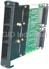
ADC PMCG-2
Description
ADC PMCG-2 Circuit Protection - Data Circuit Guard PMCG-2 - Cover - red
Part Number
PMCG-2
Price
Request Quote
Manufacturer
ADC
Lead Time
Request Quote
Category
Circuit Protection
Specifications
Cabling Type
Serial RS-232
Data Link Protocol
RS-232
Device Type
Network adapter
Form Factor
Plug-in module
Interface (Bus) Type
Expansion slot
Datasheet

Extracted Text
ADCP-50-305 Issue 9 April 2000 ™ PatchMate EIA-232/V.24, X.21, EIA-530 and V.35 Digital Patching User Manual COMP COMP MODEM MODEM MON MON 4421-A COMP COMP MODEM MODEM MON MON 4422-A 1105696 Rev A ADCP-50-305 • Issue 9 • April 2000 • Preface COPYRIGHT 1981, 1983, 1984, 1985, 1986, 1987, 1988, 1990, 1992, 1993, 1994, 1995, 1996, 1998, 1999, 2000, ADC Telecommunications, Inc. All Rights Reserved Printed in the U.S.A. TRADEMARK INFORMATION PatchMate is a trademark of ADC Telecommunications, Inc. DISCLAIMER OF LIABILITY Contents herein are current as of the date of publication. ADC reserves the right to change the contents without prior notice. In no event shall ADC be liable for any damages resulting from loss of data, loss of use, or loss of profits and ADC further disclaims any and all liability for indirect, incidental, special, consequential or other similar damages. This disclaimer of liability applies to all products, publications and services during and after the warranty period. This publication may be verified at any time by contacting ADC’s Technical Assistance Center at 1-800-366-3891, extension 3223 (in U.S.A. or Canada) or 952-946-3223 (outside U.S.A. and Canada), or by writing to ADC Telecommunications, Inc., Attn: Technical Assistance Center, Mail Station #77, P.O. Box 1101, Minneapolis, MN 55440-1101, U.S.A. ADC Telecommunications, Inc. P.O. Box 1101, Minneapolis, Minnesota 55440-1101 In U.S.A. and Canada: 1-800-366-3891 Outside U.S.A. and Canada: (952) 938-8080 Fax: (952) 946-3292 Page ii ADCP-50-305 • Issue 9 • April 2000 • Preface REVISION HISTORY EDITION/ISSUE DATE REASON FOR CHANGE 1st Edition/Issue 1 08/1981 Original. 2nd Edition/Issue 1 05/1983 Technical changes. 3rd Edition/Issue 1 12/1984 Incorporated PMBP-1 and PMBP-2 Breakout Modules; and PIMMLA-2 and PMME-2 Test Modules. 3rd Edition/Issue 2 11/1985 Changed pin numbers shown on Page 2-6 and in Table 2-1. 3rd Edition/Issue 3 02/1986 Incorporation V.35 conversion backplane. 4th Edition/Issue 1 12/1986 V.35 Pin Assignments. 5th Edition/Issue 1 12/1987 Removed reference to RS-232C and included RS-232D Pin Assignments. Merged in ADCP-50-306 Field Modification Manual. Added V.35 Module and Connector Subboard. 5th Edition/Issue 2 06/1988 Added caution statements in Section 5. 5th Edition/Issue 3 10/1988 To show connector references in Figures 3-4, 3-5, 3-7, and 3-8. 6th Edition/Issue 1 05/1990 Add information on new PMMLA-1 and PMMLA-2 Patch Modules. Add DMPS-5/48 Power Supply. 7th Edition/Issue 1 11/1990 Technical changes and added PatchMate X.21 section. 8th Edition/Issue 1 06/1992 Technical changes and update catalog numbers. 8th Edition/Issue 2 03/1993 Corrected photos and Figure 3-8. 9th Edition/Issue 1 03/1994 Replaced RS-232 with EIA-232. Added EIA-530. 9th Edition/Issue 2 03/1995 Corrected Figure 5-5. 9th Edition/Issue 3 05/1995 Added pinouts for Berg strap connections on PBC and other changes listed below. 9th Edition/Issue 4 04/1996 Clarified audible alarm feature and corrected a pin-out table. 9th Edition/Issue 5 07/1996 Change method of resetting X.21 modules. 9th Edition/Issue 6 07/1998 Updated to show new ADC corporate address and General Information. 9th Edition/Issue 7 02/1999 Revised the General Information section and updated manual to current format standards. 9th Edition/Issue 8 11/1999 Corrected Figure 5-3. 9th Edition/Issue 9 04/2000 Update Power Connection LIST OF CHANGES The technical changes incorporated into this issue are listed below. SECTION IDENTIFIER DESCRIPTION OF CHANGE 7 Pp 7-3 to 7-7 Clarify Power Connection information. Page iii 2000, ADC Telecommunications, Inc. ADCP-50-305 • Issue 9 • April 2000 • Preface Page iv 2000, ADC Telecommunications, Inc. ADCP-50-305 • Issue 9 • April 2000 • Preface TABLE OF CONTENTS Content Page FRONT MATTER ABOUT THIS MANUAL ...................................................................... ix ADMONISHMENTS......................................................................... ix SECTION 1 INTRODUCTION 1 GENERAL......................................................................... 1-1 2 PRODUCT OFFERING................................................................. 1-3 3 PATCH CORDS AND ACCESSORIES........................................................ 1-6 SECTION 2 FUNCTIONAL DESCRIPTION 1 GENERAL......................................................................... 2-1 2 PATCH MODULES ................................................................... 2-1 3 ALARMING........................................................................ 2-3 4 ALARMS ON FUNCTIONS OTHER THAN DCD ................................................. 2-6 5 STATUS INDICATORS................................................................ 2-12 6 EIA-232 PATCHMATE INTERFACE MODULE ................................................. 2-13 7 REMOTE ALARM INDICATOR PANEL...................................................... 2-13 8 EIA-232 BREAKOUT MODULE .......................................................... 2-13 9 EIA-232 TEST MODULE .............................................................. 2-15 10 PATCH BLANK PANEL ............................................................... 2-16 11 V.35 CONVERSION BACKPLANE......................................................... 2-16 12 PATCH CORDS .................................................................... 2-16 SECTION 3 PATCHMATE V.35 1 PRODUCT OFFERING................................................................. 3-1 2 APPLICATION WITH EXISTING UNITS ...................................................... 3-2 3 FUNCTION SELECTION — MODULES ...................................................... 3-5 4 FUNCTION SELECTION — CONNECTOR SUBBOARD ............................................ 3-6 5 HARDWARE INSTALLATION ............................................................ 3-8 6 RECOMMENDED MATING CONNECTOR PARTS............................................... 3-10 SECTION 4 PATCHMATE X.21 1 GENERAL......................................................................... 4-1 2 DESCRIPTION...................................................................... 4-1 3 POWER REQUIREMENTS .............................................................. 4-7 4 SPECIFICATIONS.................................................................... 4-7 5 LED/ALARM MODULE (E1 TO E6 PINS) .................................................... 4-7 6 INSTALLATION ..................................................................... 4-8 Page v 2000, ADC Telecommunications, Inc. ADCP-50-305 • Issue 9 • April 2000 • Preface TABLE OF CONTENTS Content Page SECTION 5 PATCHMATE EIA 530 PATCH MODULES 1 GENERAL .........................................................................5-1 2 MODULE DESCRIPTION................................................................5-2 3 FUNCTIONAL DESCRIPTION.............................................................5-3 4 PATCH CORDS.....................................................................5-11 5 INSTALLATION.....................................................................5-11 6 CABLE CONNECTIONS................................................................5-11 7 SPECIFICATIONS ...................................................................5-12 SECTION 6 SITE PREPARATION 1 GENERAL .........................................................................6-1 SECTION 7 INSTALLATION 1 GENERAL .........................................................................7-1 2 PATCHMATE MODULE INSTALLATION ......................................................7-1 3 PATCHMATE CHASSIS INSTALLATION......................................................7-2 4 DATA NETWORK INTERFACING...........................................................7-2 5 POWER CONNECTIONS................................................................7-3 6 REMOTE ALARM INDICATOR PANEL INSTALLATION.............................................7-6 SECTION 8 OPERATION 1 GENERAL .........................................................................8-1 2 MONITOR MODE ....................................................................8-1 3 PATCH MODE ......................................................................8-1 4 TEST MODULE......................................................................8-2 5 BREAKOUT MODULE..................................................................8-2 6 V.35 CONVERSION BACKPLANE ..........................................................8-3 SECTION 9 GENERAL INFORMATION 1 WARRANTY/SOFTWARE ...............................................................9-1 2 REPAIR/ADVANCE REPLACEMENT POLICY ...................................................9-1 3 REPAIR CHARGES ...................................................................9-2 4 REPLACEMENT/SPARE PRODUCTS ........................................................9-2 5 RETURNED MATERIAL ................................................................9-2 6 CUSTOMER INFORMATION AND ASSISTANCE.................................................9-3 Page vi 2000, ADC Telecommunications, Inc. ADCP-50-305 • Issue 9 • April 2000 • Preface TABLE OF CONTENTS Content Page FIGURES 1-1. SINGLE CIRCUIT BLOCK DIAGRAM........................................................ 1-2 1-2. PATCHMATE EIA-232/V.24 PATCH MODULES................................................. 1-2 1-3. PATCHMATE EIA-232/V.24 INTERFACE MODULES.............................................. 1-4 1-4. PMAP-1 MODULE ................................................................... 1-4 1-5. PATCHMATE BREAKOUT MODULES ....................................................... 1-5 1-6. PATCHMATE EIA-232/V.24 TEST MODULES.................................................. 1-5 1-7. V.35 CONVERSION BACKPLANE.......................................................... 1-6 2-1. PATCHMATE PATCH MODULE CIRCUIT DIAGRAM.............................................. 2-3 2-2. ALARM/STATUS CIRCUIT DIAGRAM....................................................... 2-3 2-3. ALARM CIRCUITS MODIFICATION POINTS WITH “BERG POSTS” .................................. 2-7 2-4. ALARM CIRCUITS MODIFICATION POINTS WITH SOLDER CONNECTIONS ON PC BOARDS 2-40793-0010 AND -1000 ... 2-8 2-5. ALARM CIRCUITS MODIFICATION POINTS WITH SOLDER CONNECTIONS ON PC BOARD 2-40793-1005.......... 2-9 2-6. ALARM CIRCUITS MODIFICATION POINTS WITH MINI-JUMPERS ON PC BOARDS 2-42932-9734 AND -9739...... 2-11 2-7. PATCHMATE INTERFACE MODULE CIRCUIT DIAGRAM.......................................... 2-12 2-8. PATCHMATE BREAKOUT MODULES (PMBP-1 AND PMBP-2)...................................... 2-14 2-9. PATCHMATE TEST MODULES (PIMMLA-2 AND PMME-2) ........................................ 2-15 3-1. V.35 PATCHMATE MODULES............................................................ 3-2 3-2. V.35 PATCHMATE CONNECTOR SUBBOARD.................................................. 3-3 3-3. V.35 PATCHMATE CHASSIS ............................................................ 3-3 3-4. PATCH MODULE AND CONNECTOR SUBBOARD ............................................... 3-4 3-5. INTERFACE MODULE AND CONNECTOR SUBBOARD ............................................ 3-4 3-6. PMMLA-V35 OR PIMMLA-V35 MODULE PC BOARD (COMPONENT SIDE) .............................. 3-5 3-7. PMO-516001 CONNECTOR SUBBOARD..................................................... 3-6 3-8. PMO-513001 CONNECTOR SUBBOARD..................................................... 3-7 3-9. PMCH CHASSIS READY FOR SUBBOARDS................................................... 3-9 4-1. X.21 STATUS MODULE BLOCK DIAGRAM ................................................... 4-2 4-2. X.21 LED/ALARM MODULE BLOCK DIAGRAM................................................. 4-2 4-3. X.21 LED/ALARM MODULE B ALARM ENABLE/DISABLE JUMPER STRAP LOCATION....................... 4-5 4-4. X.21 STATUS MODULE B ALARM ENABLE/DISABLE JUMPER STRAP LOCATION.......................... 4-6 4-5. X.21 LED/ALARM MODULE E1 TO E6 PIN LOCATION............................................ 4-8 5-1. PATCHMATE EIA-530 LED AND NON-LED PATCH MODULES ....................................... 5-1 5-2. PATCHMATE EIA-530 LED AND NON-LED FUNCTIONAL DIAGRAMS .................................. 5-2 5-3. PATCHMATE EIA-530 MODULE WIRING DIAGRAM ............................................. 5-4 5-4. PATCHMATE EIA-530 TEST MODULE ...................................................... 5-5 5-5. PATCHMATE EIA-530 SIGNAL CONNECTIONS................................................. 5-5 5-6. PATCHMATE EIA-530 LED PATCH MODULE .................................................. 5-6 5-7. PATCHMATE EIA-530 “B” LEAD CONNECTIONS ............................................... 5-7 5-8. PATCHMATE EIA-530 TRANSMIT TIMING STRAPS ............................................. 5-8 5-9. PATCHMATE EIA-530 PMM-636003 TEST MODULE............................................. 5-9 5-10. PATCHMATE EIA-530 TEST MODULE WIRING AND PIN ASSIGNMENTS............................... 5-10 7-1. POWER CONNECTIONS ............................................................... 7-3 7-2. DC POWER INTERFACE BRACKET INSTALLED IN CHASSIS........................................ 7-6 Page vii 2000, ADC Telecommunications, Inc. ADCP-50-305 • Issue 9 • April 2000 • Preface TABLE OF CONTENTS Content Page TABLES 1-1. PATCHMATE COMPONENTS.............................................................1-6 1-2. STANDARD PATCH CORDS AND ACCESSORIES................................................1-9 2-1. EIA-232 PIN ASSIGNMENTS.............................................................2-2 2-2. ALARM TIME DELAY SETTINGS ..........................................................2-5 2-3. EXTERNAL ALARM OUTPUT SPECIFICATIONS.................................................2-5 2-4. PC BOARD MODIFICATIONS.............................................................2-6 2-5. LED STATUS INDICATORS.............................................................2-12 2-6. V.35 POSITION WIRING...............................................................2-17 3-1. PRODUCT DESCRIPTION...............................................................3-1 3-2. OPTIONAL ITEMS ON THE MODULES.......................................................3-5 3-3. OPTIONAL ITEMS ON THE CONNECTOR SUBBOARD.............................................3-6 3-4. CONNECTIONS ON THE BACKPLANE ADAPTER FOR USING UNASSIGNED PINS...........................3-7 3-5. NORMAL PIN ASSIGNMENTS ............................................................3-8 4-1. SIGNAL STATUS.....................................................................4-3 4-2. STATUS MODULE A ALARM TIME DELAY SETTINGS.............................................4-4 4-3. STATUS AND LED/ALARM MODULE B ALARM TIME DELAY SETTINGS.................................4-4 4-4. LED/ALARM MODULE A ALARM TIME DELAY SETTINGS..........................................4-5 4-5. QUIESCENT STATE INDICATORS..........................................................4-6 4-6. SPECIFICATIONS ....................................................................4-7 5-1. SIGNAL CONNECTIONS................................................................5-8 5-2. MODULE SPECIFICATIONS.............................................................5-12 Page viii 2000, ADC Telecommunications, Inc. ADCP-50-305 • Issue 9 • April 2000 • Preface ABOUT THIS MANUAL ™ This manual was written for users of ADC PatchMate network analysis and restoral systems. It contains installation and operation procedures for EIA-232/V.24, X.21 and V.35 digital patching and monitoring circuits. This manual brifly describes the PatchMate system and its components, explicitly states the site and installation requirements, and lists the operating procedures. ADMONISHMENTS Important safety admonishments are used throughout this manual to warn of possible hazards to persons or equipment. An admonishment identifies a possible hazard and then explains what may happen if the hazard is not avoided. The admonishments — in the form of Dangers, Warnings, and Cautions — must be followed at all times. These warnings are flagged by use of the triangular alert icon (seen below), and are listed in descending order of severity of injury or damage and likelihood of occurrence. Danger: Danger is used to indicate the presence of a hazard that will cause severe personal injury, death, or substantial property damage if the hazard is not avoided. Warning: Warning is used to indicate the presence of a hazard that can cause severe personal injury, death, or substantial property damage if the hazard is not avoided. Caution: Caution is used to indicate the presence of a hazard that will or can cause minor personal injury or property damage if the hazard is not avoided. Page ix 2000, ADC Telecommunications, Inc. ADCP-50-305 • Issue 9 • April 2000 • Preface COMP COMP MODEM MODEM MON MON 4421-A With Status Indicators and Alarm COMP COMP MODEM MODEM MON MON 4422-A Without Status Indicators and Alarm PATCHMATE EIA-232/V.24 DIGITAL PATCHING Page x 2000, ADC Telecommunications, Inc. INTRODUCTION ADCP-50-305 • Issue 9 April 2000 Section 1: Introduction SECTION 1: INTRODUCTION Content Page 1 GENERAL......................................................................... 1-1 2 PRODUCT OFFERING................................................................. 1-3 3 PATCH CORDS AND ACCESSORIES........................................................ 1-6 1 GENERAL This section lists the product line features and describes the different components of the PatchMate EIA-232 (or CCITT V.24) Digital Patching System. The PatchMate System provides convenient access to EIA-232 (or CCITT V.24) serial binary data interchange circuits for patching, monitoring, testing or reconfiguring a data communications network. The PatchMate product line is a flexible, modular system providing the following features: • Monitoring of digital serial binary data interchange circuits without circuit interruption. Line access on an EIA-232 digital serial binary data interchange circuit either toward the Data Terminal Equipment (DTE) or the Data Communications Equipment (DCE). Alarming identifies the circuit in trouble with both a visual and audible warning. PatchMate Modules can be equipped with female connectors on both DCE and DTE or standard male DCE and female DTE connectors. Remote Alarm Indicator Panel allows PatchMate alarm status indicators to be installed up to 50 feet away from the modules. Optional breakout module with LEDs for status monitoring on 11 of the EIA-232 serial binary data interchange leads. Switches and pin jacks along with test leads are provided for test and injection of signals. It also has a pulse trap and a test LED that can be jumpered from any lead via pin jacks. A breakout module without LEDs or pulse trap is also available. Optional test module with two EIA-232 25-pin type D connectors for connecting to test equipment or spares and one 26-pin ADC PatchMate jack port for patching to serial binary data interchange circuits being tested. It is available with or without eight LED monitors. Flexibility of the modular system allows the addition of modules or the interchanging of modules on a single line basis. High density chassis occupies 5.25 inches (13.3 cm) in height within a standard 19-inch (48.3 cm) wide rack. Each rack-mounted PatchMate chassis has 18 module positions. Typically, a chassis contains 16 modules and reserves the two right-most chassis slots for special modules. Currently, the PatchMate Interface Module or PatchMate Test Module can fill the seventeenth position. The seventeenth and eighteenth slot can be filled with a PatchMate Breakout or they can be filled with PatchMate blank panels. Page 1-1 2000, ADC Telecommunications, Inc. 0 A L F L E DLY F M D RST ALM TD RD DCD SQ RTS CTS DSR DTR ADCP-50-305 Issue 9 April 2000 Section 1: Introduction Each PatchMate module within a chassis is dedicated to one EIA-232 (or CCITT V.24) serial binary data interchange circuit (see Figure 1-1). The rear edge of each patch module incorporates two standard 25-pin connectors for interfacing the digital serial binary interchange circuit. The front panel of each PatchMate module (see Figure 1-2) presents three jacks through which the digital circuit can be accessed. With no patch cords inserted into the front panel jacks, the attached EIA-232/V.24 circuit has a non-interrupted path through the PatchMate module. When the connector of the patch cord is inserted into either the top or middle front panel jack, the digital circuit is split and routed through the patch cord. The other connector can then be inserted into another jack, and in so doing, a different device (e.g., spare modem, a different computer port) can be attached to the digital circuit. The bottom front panel jack provides bridged, non-interference monitoring of the attached circuit. Insertion of a PatchMate patch cord into the bottom front panel jack allows the attachment of a diagnostics device (e.g., a data line monitor). FEP CPU FRONT PANEL DTE JACKS PATCH MODULE (SIDE VIEW) DCE VF MODEM TO REMOTE SITE 4407-A Figure 1-1. Single Circuit Block Diagram PMM-1 PMMLA-1 4493-A 4494-A Figure 1-2. PatchMate EIA-232/V.24 Patch Modules Page 1-2 2000, ADC Telecommunications, Inc. ADCP-50-305 Issue 9 April 2000 Section 1: Introduction 2 PRODUCT OFFERING The PatchMate EIA-232/V.24 Patching product family contains two types of data patch modules and three types of chassis. Both models of patching modules contain the access and monitor features described in the preceding paragraph. The PMM-1 Patch Module (shown in Figure 1-2) and the PMM-2 Patch Module contain the basic circuitry to provide the stated features and require no external power. The PMM-1 Patch Module has two female connectors on the rear edge and the PMM-2 Patch Module has a female DTE connector and a male DCE connector. Typically, the PMM-1 and PMM-2 Patch Modules plug into the PMCH-2 PatchMate Chassis. The PMCH-2 chassis contains no power supply and therefore requires no external electrical connections. The second type of patch module contains LEDs and alarm detection circuits. The PMMLA-1 Patch Module and the PMMLA-2 Patch Module contain all of the features of the PMM-1 module plus eight LED status indicators, an alarm indicator, and loss of carrier alarm circuitry. The PMMLA-1 Patch Module has two female connectors on the rear edge and the PMMLA-2 Patch Module has a female DTE connector and a male DCE connector. The PMMLA-1 and the PMMLA-2 modules require external power, and consequently these modules must be mounted within a PMCH-1 or PMCH-3 PatchMate chassis, equipped with power supply, in order for the status and alarm options to function. Modules built prior to 1990 that monitor other than DCD (Data Carrier Detect) are equipped to alarm on the signal voltage conditions of TD, RD, SQ, RS, CS, DSR, DTR, TC, RC, and ETC. PMMLA-1 and PMMLA-2 modules may be modified in the field to alarm on any lead. Details of this modification are given in Section 2 of this manual. Modules built beginning in 1990 allow user selectable alarming on loss or continued presence of any one of the eight monitored signals. In addition to the patch modules, the PatchMate chassis may contain three other types of modules. They are the Interface, Test and Breakout modules. The PMME-1 (see Figure 1-3) is a PatchMate Interface Module. This unit is used when any device having EIA-232/V.24 connectors, such as test equipment, need to be patched in at the front panel. The PMME-1 provides patch cord jacks on the front panel and EIA-232/V.24 connectors on the back for any such equipment to be readily accessed. A second type of interface module (PIMMLA-1, see Figure 1-3) has eight LED status indicators with an alarm indicator. A test module (PIMMLA- 2) is shown in Figure 1-6. This module contains an EIA-232/V.24 “D” type male connector on the back as well as a 26-pin patch jack on the front. Both connectors and the patch jack are connected in parallel for ease in testing. The PIMMLA-2 module has eight LEDs on the front with an alarm indicator. This module is also available without the LEDs and alarm as a PMME-2 (see Figure 1-6). Both the PIMMLA-1 and the PIMMLA-2 modules have user selectable alarming on loss or continued presence of any one of the eight monitored signals. The Breakout Modules (PMBP-1 and PMBP-2) shown in Figure 1-5 are described later in this section. A blank panel (PMBF-1) is available to fill in unused slots in the PatchMate chassis. The PMAP-1 Remote Alarm Indicator Panel displays the alarm conditions of all Patch and Alarm Interface Modules in a PMCH-3 Patch Chassis. Figure 1-4 show the PMAP-1 Remote Alarm Indicator Panel. The PMCH-3 Patch Chassis is a powered chassis, similar to the PMCH-1 Patch Chassis with the alarm output from each card position wired to a connector at the rear of the chassis. A Remote Alarm Indicator Panel has 18 LED indicators, one for each card position in the patch chassis. A cable, 50 feet (15.2 m) maximum, connects each Remote Alarm Indicator Panel with the associated remote patch chassis. The Remote Alarm Indicator Panel (PMAP-1, see Figure 1-4) may be mounted in a non-powered (PMCH-2) chassis as well as in a powered (PMCH-1) chassis. Page 1-3 2000, ADC Telecommunications, Inc. 0 A L F L E DLY F M D RST RESET ALM 15 18 TD RD DCD SQ RTS CTS DSR DTR 1 5 10 ADCP-50-305 Issue 9 April 2000 Section 1: Introduction PMME-1 PIMMLA-1 4495-A 4496-A Figure 1-3. PatchMate EIA-232/V.24 Interface Modules 4497-A Figure 1-4. PMAP-1 Module The PatchMate product family also offers two types of breakout modules, PMBP-1 and PMBP-2 (see Figure 1-5). Either one is normally mounted in slot position 17 and 18 of the PatchMate chassis. Both units contain two patch jack ports on the front, marked DTE and DCE along with 24 switches numbered 2 through 25. (Lead 1 is the Frame Ground and is never opened.) On either side of the switches are associated pin jacks labeled DTE and DCE. The breakout module enables the user to change signal path for one or all of the 24 circuit leads. The signal path is changed by connecting the appropriate jumper wires provided between pin jacks. Page 1-4 2000, ADC Telecommunications, Inc. O O O N N N OPEN OPEN OPEN 1 2 3 4 5 6 7 8 1 2 3 4 5 6 7 8 1 2 3 4 5 6 7 8 DTE DCE DCE 2 3 4 5 6 7 8 9 10 11 12 13 14 14 16 17 18 19 20 21 22 23 24 25 DTE DTE DCE 2 3 4 5 6 7 8 9 10 11 12 13 14 14 16 17 18 19 20 21 22 23 24 25 DTE DCE DCE BREAKOUT 0 A L F L E DLY F M D RTS DTR SQ TEST G +5 CTS ETC TC DSR DCD TRAP TRP RST RC TD RD DTE DTE DCE BREAKOUT RST ALM TD RD DCD SQ RTS CTS DSR DTR ADCP-50-305 Issue 9 April 2000 Section 1: Introduction Breakout module PMBP-2 includes lead status monitoring and signal trapping capabilities. The front panel (see Figure 1-5) contains 11 LEDs plus a TEST LED and a TRAP LED along with a trap reset toggle switch (TRP RST), two patch jack ports and 24 switches. The 11 EIA-232/V.24 circuit leads monitored for status include: RS, DTR, SQ, CS, ETC, TC, DSR, RC, TD, and RD. A TEST LED can be connected by jumper to any of the 24 signal leads. This LED will light if some signal voltage condition comes on and will go out if the voltage condition goes away. A TRAP LED is also provided and can be connected by jumper to any of the 24 leads. This LED will also light if some signal voltage condition comes on but it will stay lit, even if the voltage condition goes away, until the trap reset (TRP RST) button is pushed. PMBP-2 PMBP-1 4498-A 4499-A Figure 1-5. PatchMate Breakout Modules The two types of test modules are the PIMMLA-2 and PMME-2. Test module PIMMLA-2, shown in Figure 1-6, may be mounted in any slot of PMCH-1, PMCH-2, or PMCH-3. However, if PIMMLA-2 is mounted in a PMCH-2, a DMPS-11/11E power supply is required. This module provides the user with EIA-232/V.24 interface capabilities, status monitoring for eight lead and alarm conditions. PIMMLA-2 PMME-2 4500-A 4501-A Figure 1-6. PatchMate EIA-232/V.24 Test Modules Page 1-5 2000, ADC Telecommunications, Inc. ADCP-50-305 Issue 9 April 2000 Section 1: Introduction The PIMMLA-2 Test Module contains two EIA-232/V.24 ports (female on the front panel and male on the rear of the module) and a patch jack. The eight EIA-232/V.24 leads monitored for status include: TD, RD, DCD, SQ, RS, CS, DSR, and DTR. Each lead contains an associated LED indicator, located on the front panel, that turns on when the signal is active (or high). An adjustable alarm circuit with associated LED (ALM) is also provided to inform the user when a pre-selected alarm condition exists. After an alarm condition occurs, the alarm circuit may be reset by the operator touching the finger reset (RST) switch. A toggle switch is also provided to enable/disable the alarm LED. Test module PMME-2, also shown in Figure 1-6, may be mounted in any slot of PMCH-1, PMCH-2 or PMCH-3. No power is required. This module is identical to the PIMMLA-2, but without monitoring or alarm circuitry. The V.35 Conversion Backplane (PMBP-V.35), shown in Figure 1-7, mounts on any of the standard EIA-232/V.24 PatchMate chassis to house adapter cables providing V.35 connections for DCE and DTE PatchMate connectors. Up to 36 adapter cables can be mounted on the backplane, providing a V.35 appearance with a 25-pin “D” type subminiature connector that is then connected to the rear of a PMM-1 or PMM-2 Patch Module installed in the chassis. This device is for use with NON-LED modules only. Table 1-1 lists the different PatchMate Patch Modules and Chassis. 4526-A Figure 1-7. V.35 Conversion Backplane 3 PATCH CORDS AND ACCESSORIES Table 1-2 details standard patch cords and accessories available for use with PatchMate products. Table 1-1. PatchMate Components MODEL # DESCRIPTION COMMENTS PMBP-1 Breakout Module Requires two slot positions in PMCH-1, PMCH-2, or PMCH-3. PMBP-2 Breakout Module Same as PMBP-1 and provides complete breakout box Includes 11 LEDs for status capabilities. If used in PMCH-2, a DMPS-11/11E power monitoring and two LEDs supply is required. for the Trap and Test LED PMM-1 Patch Module Unit contains no LEDs or alarm and does not require a powered chassis. (continued) Page 1-6 2000, ADC Telecommunications, Inc. ADCP-50-305 Issue 9 April 2000 Section 1: Introduction Table 1-1. PatchMate Components, continued MODEL # DESCRIPTION COMMENTS PMM-2 Patch Module Same as PMM-1 except with male DCE connector. PMML-1 Patch Module Unit contains LEDs without alarms and requires a powered chassis. PMML-2 Patch Module Same as PMML-1, except with male DCE connector. PMMLA-1 Patch Module Unit contains LEDs/alarms and requires a powered chassis. PMMLA-2 Patch Module Same as PMMLA-1, except with male DCE connector. PMME-1 Patch Interface Module Unit mounts into the seventeenth chassis position. Contains no LEDs or alarm and does not require a powered chassis. PMME-2 Test Module Same as PIMMLA-2, but without LEDs and alarm circuitry. PIMMLA-1 Patch Interface Module Unit mounts into the seventeenth chassis position. Contains LEDs/alarm and does require a powered chassis. Alarm circuitry is user selectable. PIMMLA-2 Test Module. Includes eight Provides an interface port for test equipment LEDs for lead status requiring EIA-232/V.24 circuit compatibility. monitoring, an adjustable Mounts in any slot in PMCH-1 or PMCH-3. alarm and a patch jack port. If used in PMCH-2, a DMPS-11/11E power supply is required. PMME-X21 X.21 Interface Module Unit mounts in the seventeenth chassis position. Contains no LEDs or alarm and does not require a powered chassis. Equipped with female DB 15 connectors. PMM-830001 X.21 Test/Status Module Provides an interface port for test equipment Includes six LEDs for status requiring X.21 circuit compatibility. Mounts indication, six LEDs for in any two slots in the PMCH-1, PMCH-2, quiescent state indication or PMCH-3 chassis. If used in PMCH-2, and a dual alarming DMPS-11/11E power supply is required. function. PMMLA-V35 V.35 Patch Module Unit contains LEDs/alarm and requires a powered chassis. PMM-V35 V.35 Patch Module Same as PMMLA-V.35, except without LEDs and alarms. PMMLA-V35FF V.35 Patch Module Same as PMLA-V.35, except two female connectors. PMM-V35FF V.35 Patch Module Same as PMM-V.35, except two female connectors. PMMLA-V35 V.35 Patch Module Same as PMMLA-V.35 except two female connectors. PMM-V36FF V.35 Patch Module Same as PMM-V.35 except two female connectors. (continued) Page 1-7 2000, ADC Telecommunications, Inc. ADCP-50-305 Issue 9 April 2000 Section 1: Introduction Table 1-1. PatchMate Components, continued MODEL # DESCRIPTION COMMENTS PIMMLA-V35 V.35 Interface Module Unit mounts in the seventeenth chassis position. Contains LEDs/alarm and does require a powered chassis. Alarm circuit is user selectable. PMME-V35 V.35 Interface Module Same as PIMMLA-V.35, except without LEDs and alarms. PMO-516001 V.35 Subboard PatchMate subboard with male/female V.35 plugs on the back and a 56-pin card edge connector on the front. Provided with the V.35 Patch Module. PMO-513001 V.35 Subboard PatchMate subboard with male/female V.35 plugs on the back and a 56 pin card edge connector on the front. Provided with the V.35 Interface Module. PMM-614001 EIA-530 Patch Module The EIA-530 patch module mounts into the standard PMCH-1 or PMCH-7 PatchMate powered chassis. Dual colored LEDs provide passive monitoring of the EIA 530 signal leads. PMM-616004 EIA-530 Patch Module Same as the PMM-614001 except without the LED monitoring. Mounts into the standard PMCH-2 non- powered PatchMate chassis. PMM-636003 EIA-530 Test Module Provides an interface port for test equipment requiring EIA-530 circuit compatibility. Mounts in any slot in PMCH-1 or PMCH-7. If used in PMCH-2, a DMPS- 11 power supply is required. PMCH-1 Patch Chassis Standard rack mounted chassis with power supply. Chassis can hold up to 16 Patch Modules and/or two other modules (Interface, Test, or Breakout Modules). PMCH-2 Patch Chassis Same as PMCH-1, but has no power supply and does not support audible alarms. PMCH-3 Patch Chassis Same as PMCH-1, plus equipped with alarm feature for us with remote Alarm Indicator Panel PMAP-1. PMCH-7 Patch Chassis Same as PMCH-1, but has no audible alarm circuitry. PMAP-1 Remote Alarm Contains 18 alarm LEDs. Used in a central location Indicator Panel to bring in alarm leads from PMCH-3 chassis up to 50 feet away. Includes a 50 foot cable. PMBP-V35 Conversion Backplane Provide housing for V.35 adapter cables. PMBP-AC-MF V.35 Adapter Cable pair with male 24 pin female V.35 connector for use with PMM-1 module and male V.35 cables. PMBP-AC-FF V.35 Adapter Cable pair with female 25 pin and female V.35. PMBP-AC-FM V.35 Adapter Cable pair with female 25 pin and male V.35 for use with PMM-2 modules. PMBP-AC-MM V.35 Adapter Cable pair with male 25pin and male DMPS-5 Power Supply Power supply used with a PMCH-1 or PMCH-3 chassis when110 Vac/60 Hz is available DMPS-5A Power Supply Same as the DMPS-5 except has a 110V extension cord for plugging into local electrical outlet. (continued) Page 1-8 2000, ADC Telecommunications, Inc. ADCP-50-305 Issue 9 April 2000 Section 1: Introduction Table 1-1. PatchMate Components, continued MODEL # DESCRIPTION COMMENTS DMPS-5E Power Supply Power supply used with a PMCH-1 or PMCH-3 chassis when 220 Vac/50 Hz is available. DMPS-11/11E Power Supply Power supply used with PMCH-2 when PMBP-2 Breakout Module or PIMMLA-2 Test Module is installed. DMPS-5/48 Power Supply Power supply used with a PMCH-1 or PMCH-3 chassis when–48 Vdc is available. Table 1-2. Standard Patch Cords and Accessories MODEL # DESCRIPTION COMMENTS PMPC-X Patch Cord Standard 1-to-1 PatchMate Patch Cord. X = length in feet. Available in 2-, 3-, 4-, 6-, 8-, and 10-foot lengths. PMPC-B-X Balanced Patch Cord Balanced PatchMate Patch Cord featuring shielded twisted pair cable. Recommended for using with balanced interfaces such as EIA-422. Available in 2-, 3-, 4-, 6-, 8-, and 10-foot lengths. PMPC-BV-X Patch Cord Same as PMPC-B-X, except for use with V.35 interface. PM-MM-PC-X Modem Eliminator Similar to PMPC, but crosses pins 2 and 3, shunts pins Patch Cord 4 and 5, shunts pins 6 and 8, and crosses pins 8 and 20. Available in 1-, 2-, 3-, 4-, 6-, 8-, and 10-foot lengths. PMCPC-F-X Female 25-Pin to Provides a female 25-pin “D” type subminiature PatchMate Patch Cord connector at one end of a standard patch cord. Available in 6- and 10-foot lengths. PMCPC-M-X Male 25-Pin to Similar to PMCPC-F-X, but uses a male 25-pin “D” PatchMate Patch Cord type subminiature connectors. Available in 6- and 10-foot lengths. EIA-530 Patch Patch Cord A1 to 1 EIA 530 patch cord used with the EIA-530 Cord Patch Module. EIA-530 Modem Null Modem Patch Provides “Loopback” connections between two DTEs Cord or DCEs. EIA-530-DB 25 Female 25-Pin to Provides a female 25-pin “D” Type Subminiature Patch Cord PatchMate Patch Cord Connector at one end of a standard patch cord. Available in 2, 4, 6, and 8 foot lengths. PMLP-4 Looping Plug Inserts in patch receptacle and connects pins 2 to 3, 14 to 19, 17 to 24, 18 to 23. PMLP-5 Looping Plug Similar to PMLP-4, but loops only 2 to 3 and 15 to 17. PMCG-1 Circuit Guard red Inserts in patch receptacle without breaking circuit. designator Prevents inadvertent patching. PMCG-2 Circuit Guard white Similar to PMCG-1, but contains white designator. designator white designator. Page 1-9 2000, ADC Telecommunications, Inc. FUNCTIONAL DESCRIPTION ADCP-50-305 • Issue 9 April 2000 Section 2: Functional Description SECTION 2: FUNCTIONAL DESCRIPTION Content Page 1 GENERAL......................................................................... 2-1 2 PATCH MODULES ................................................................... 2-1 3 ALARMING........................................................................ 2-3 4 ALARMS ON FUNCTIONS OTHER THAN DCD ................................................. 2-6 5 STATUS INDICATORS................................................................ 2-12 6 EIA-232 PATCHMATE INTERFACE MODULE ................................................. 2-13 7 REMOTE ALARM INDICATOR PANEL...................................................... 2-13 8 EIA-232 BREAKOUT MODULE .......................................................... 2-13 9 EIA-232 TEST MODULE .............................................................. 2-15 10 PATCH BLANK PANEL ............................................................... 2-16 11 V.35 CONVERSION BACKPLANE......................................................... 2-16 12 PATCH CORDS .................................................................... 2-16 1 GENERAL This section describes how each component in the PatchMate EAI-232/V.24 Patching product family functionally operates within a data communications network. The PatchMate patch modules allow the monitoring and/or patching of up to 25 leads of a single EIA-232/V.24 serial binary data interchange circuit. Pin number 1 is connected to the patch port. You may select to have pin 1 open upon the insertion of a patch cord or always connected between pin 1 of each interface connector. Table 2-1 presents the EIA Standard EIA-232 pin assignments for reference. The PatchMate system provides physical, hard-contact access to any data circuit; and through the use of a special patch cord, the operator can directly monitor a circuit (i.e., non-interface testing); split the data circuit and test the line toward the DTE (e.g, the front-end processor) or test the line toward the DCE (e.g., the modem), and/or substitute operational components for faulty units (e.g., a spare modem for a faulty modem). 2 PATCH MODULES The PatchMate Patch Modules (i.e., the PMM-1 and PMM-2 and PMML-1 and PMMLA-2) contain three front panel jacks for easy access to the EIA-232 circuit, and two rear connectors for attaching the module to the digital circuit. Figure 2-1 presents the PatchMate Patch Module’s circuit diagram, and the following paragraphs discuss the unit’s circuitry. Typically, the PatchMate equipment is placed in the circuit between the CPU and its associated modem (refer to Figure 1-1). The two rear connectors are provided to interface the data patching equipment with the computer’s communications network. The top rear connector is used to attach the EIA-232/V.24 circuit from the DTE (e.g., a computer or front end processor), and the bottom rear connector is used to attach the circuit to the DCE (e.g., a modem). In the normal mode (i.e., no patch cords inserted into the top or middle front panel jacks), the EIA-232/V.24 circuit has a through-path into and out of the Patch module. In the normal mode, the insertion of a patch cord connector into the bottom front panel jack allows the entire circuit to be monitored with no interruption of the signals. Page 2-1 2000, ADC Telecommunications, Inc. ADCP-50-305 Issue 9 April 2000 Section 2: Functional Description In the patch mode, the insertion of a patch cord connector into the top or middle front panel jacks breaks the path through the module and splits the circuit into two parts. The top front panel jack is now used to access and/or patch the DTE portion of the circuit (i.e., the portion of the EIA-232/V.24 circuit that is connected to the top rear connector). The middle front panel jack is then used to access and/or patch the DCE portion of the circuit (i.e., the portion of the data circuit that is connected to the bottom rear connector). In the patch mode, insertion of a patch cord connector into the bottom front panel jack (i.e., the MON jack) permits the monitoring of the DCE side of the data circuit (see Figure 2-1). Table 2-1. EIA-232 Pin Assignments PIN # REFERENCE ABBREVIATION DESCRIPTION 1 AA FG Frame Ground 2 BA TD Transmitted Data 3 BB RD Received Data 4 CA RS Request To Send 5 CB CS Clear To Send 6 CC DSR Data Set Ready 7 AB SG Signal Ground 8 CR DCD Data Carrier Detect 9 Positive DC Test Voltage 10 Negative DC Test Voltage 11 Unassigned 12 SCF Secondary Received Line Detector 13 SCB SCS Secondary Clear To Send 14 SBA STD Secondary Transmitted Data 15 DB TC Transmitter Clock 16 SBB SRD Secondary Received Data 17 DD RC Received Clock 18 LL LL Local Loopback 19 SCA SRS Secondary Request To Send 20 CD DTR Data Terminal Ready 21 CG SQ Signal Quality Detect 22 CE RI Ring Indicator 23 CH/CI Data Rate Select 24 DA ETC External Transmitter Clock 25 TM TM Test Mode Page 2-2 2000, ADC Telecommunications, Inc. ADCP-50-305 Issue 9 April 2000 Section 2: Functional Description MONITOR INDICATORS CIRCUITRY COMPUTER DTE MODEM DCE MONITOR 4409-A Figure 2-1. PatchMate Patch Module Circuit Diagram 3 ALARMING The PMMLA-1 and PMMLA-2 PatchMate Modules, the PIMMLA-1 PatchMate Interface Module, and the PIMMLA-2 PatchMate Test Module contain the added features of signal monitoring alarm circuitry and LED status indicators. Both of these features are discussed in the following paragraphs. Figure 2-2 shows the circuit diagram of these features. TD PIN 2 PIN 3 RD PIN 8 DCD SQ PIN 21 RTS PIN 4 CTS PIN 5 DSR PIN 6 DTR PIN 20 PIN 7 SELECTABLE ALM ALARM RST CIRCUIT OFF CONTROL LOGIC ALM LED 7.5 Vac POWER SUPPLY DLY 4410-B Figure 2-2. Alarm/Status Circuit Diagram Page 2-3 2000, ADC Telecommunications, Inc. ADCP-50-305 Issue 9 April 2000 Section 2: Functional Description The alarm circuits are designed to provide audible and visual indications, if the signal is lost or continually present for a time longer than a preset time delay. The circuit recognizes an alarm state when any one of the eight monitored signals is lost or continually present as selected by the user. Regardless of which lead the alarm circuit is monitoring, the user can select to alarm on a voltage less than +2 Vdc that persists longer then the preset time or the presence of a voltage greater than +2 Vdc that persists longer than the preset time delay. When the alarm trips the buzzer sound, and the amber ALM (i.e., alarm) indicator lights. The alarm can be reset by touching the pads marked RST (i.e., reset); but, if the alarm condition has not cleared, the alarm will time-out, and the alarm will be tripped again. A coin or screwdriver blade touched across the RST pads may be required to reset the alarm. : The audible alarm indicator on all modules with alarming is dependent on a Note hardware “buzzer” located only in a PMCH-1 or PMCH-3 chassis. If a module is properly powered (either from the chassis, or in some cases from a DMPS-11/11E auxiliary power supply) the visual alarm (Yellow LED) will be functional, but the audible alarm function is not supported in the PMCH-2, PMCH-6, or PMCH-7 chassis. The front panel contains a three-position toggle switch that is used to activate and deactivate the alarm circuit. In the left-most position, OFF, the alarm is totally deactivated and will disregard the status of the alarm condition. In the middle position, ALM, the alarm circuit is activated and provides audible and visual indications when the alarm condition occurs. In the right-most position, LED, the alarm circuitry is activated; but, only the amber ALM LED will light when the alarm condition occurs. Independent of the last two switch positions, the alarm can be reset by touching the RST touch pads on the front panel with a coin or screwdriver blade, or the alarm can be deactivated by placing the toggle switch to the OFF position. One of the options found on modules with alarm circuitry allows the automatic reset of the alarm when the circuit returns to a positive or negative voltage greater than +3.5 Vdc (i.e., the alarm condition clears). Loss or continued presence of a monitored signal can be selected for positive or negative polarity. This polarity option can be changed by moving the mini-jumper (Berg Strap) or shorting plug found on the component side of the circuit board. Another option found on modules with alarm circuitry is the alarm latched or unlatched option. This option can be changed by moving the mini-jumper (Berg Strap) or shorting plug found on the lower center portion or center rear portion on the component side of the circuit board. If the module is optioned for latched operation, a detected alarm condition will continue to be displayed until the manual reset is activated. In the unlatched mode, a detected alarm condition will be automatically reset when circuit conditions return to normal. Modules containing alarm circuitry contain a self-test feature. This feature tests the alarm circuit, circuit continuity, buzzer deactivate circuit and reset circuitry. The self-test is initiated when the toggle switch is placed in the OFF position, which the alarm circuit recognizes as an alarm state. The next step in the self-test is to place the front panel switch in the ALM position. This action activates the buzzer and the ALM LED and verified circuit continuity between the module and the motherboard. Next, placing the toggle switch to the LED position deactivates the alarm buzzer but maintains an active LED indicator. This last action verifies that the buzzer deactivate circuit is working. The self-test procedure is terminated by touching the front panel RST pads with a coin or screwdriver blade. The extinguishing of the alarm light shows that the reset circuit is working. This self-test feature becomes nonoperative when the automatic reset option is installed. Page 2-4 2000, ADC Telecommunications, Inc. ADCP-50-305 Issue 9 April 2000 Section 2: Functional Description Another feature of modules containing alarm circuitry is a power-up reset function. This function provides the automatic reset of the alarm circuit when the power comes back on. This feature prevents the alarm from tripping when the module is initially supplied power, when brief power interruptions are encountered and when large power drops, such as during brown- out conditions occur. The front panel also contains an eight-position rotary switch that is labeled DLY. The rotary switch is used to set the alarming time delay. The values of the time delays are fixed; but, their time values depend upon the frequency of the power supply (i.e., 60 Hz or Ho Hz). Seven of the switch positions are time values ranging from 63 msec to 81.9 sec. nominal, and the eighth position is a pulse catcher setting. The seven time delay settings are denoted on the front panel by varying length arcs around the rotary switch, the longer the arc — the greater the time delay. The values of the time delays are listed in Table 2-2. The eighth position, the pulse catcher setting, is used when voltage pulse indication is desired. The pulse catcher setting recognizes a signal loss or presence of 50 µsec or greater, regardless of the power supply frequency. Table 2-2. Alarm Time Delay Settings TIME DELAY ARC 50 HZ 60 HZ OR –48 VDC LENGTH ENVIRONMENT ENVIRONMENT V 50µsec 50µsec Shortest 75 msec 63 msec 315 msec 263 msec 635 msec 529 msec 1.3 sec 1.1 sec 10.2 sec 8.5 sec 41.0 sec 34.1 sec Longest 81.9 sec 68.3 sec Modules which contain alarm circuitry normally should be housed within a powered chassis such as the PMCH-1 to take full advantage of the audible alarm provided. This type of chassis features connections for the output of an alarm signal and for the input of an external reset signal. The PMCH-1 and PMCH-3 chassis present three terminals that can be connected to provide the two external functions. The terminals are located on the side of the chassis as viewed from the rear. The contacts are labeled as follows: ALARM, SIG GND, and RESET. The contact labeled ALARM provides attachment for the external alarm. If just one module’s alarm trips within a chassis, this contact sends a signal that is an open drain output with maximum ratings as listed in Table 2-3. Table 2-3. External Alarm Output Specifications CONDITION SPECIFICATION Power Dissipation O.4 w Continuous Drain Current 0.4 A Maximum Drain to Ground Voltage 50 Vdc TTL Compatible, Alarm Output Sinkage 50 mA, at 0.5 Vdc or less Page 2-5 2000, ADC Telecommunications, Inc. ADCP-50-305 Issue 9 April 2000 Section 2: Functional Description The other pins, labeled SIG GND and RESET, are used for the master reset function. When these contacts are connected through a resistance less than 5,000 ohms, the reset pin goes to ground, which in turn resets the alarm circuits for the modules within the chassis. The master rest function can also be initiated through a hard contact to ground. 4 ALARMS ON FUNCTIONS OTHER THAN DCD The PMMLA-1 and PMMLA-2 Data Patch Module along with the PIMMLA-1 Data Interface Module and PIMMLA-2 Data Test Module have the alarm on DCD, the Data Carrier Detect lead (pin 8). The PIMMLA21-1 (manufacture discontinued) had the alarm on SQ or Signal Quality lead (pin 21). In certain applications, it may be necessary to alarm one of the other leads. Two options are available: 1. Factory protection modules. 2. Field modification to existing modules. All modules presently in production permit user selectable alarming. The customer field modification option is more involved. The procedure for the field modification is as follows: a) Several different versions of some modules exist in the field. Remove the Data Patch, Data Interface or Data Test Module from the chassis. Determine which version you have by identifying the PC Board used. It’s number can be found on the non-component side of the board, see Table 2-4. Refer to the figure shown in Table 2-4 for the modification points on the PC Board. If it refers you to the drawing in Figure 2-3, you need only position the mini-jumper to the appropriate pins on the wire wrap connectors shown. The mini-jumper needs to connect a wire in the center row to the appropriate wire in the top or bottom row (shown on DCD in the insert in Figure 2-3). This completes the modification. If Table 2-4 refers you to the drawing in Figure 2-4, proceed with Step “b.” If Table 2-4 refers you to the drawing in Figure 2-5, go to Step “k” for modification instructions. If Table 2-4 refers you to the drawing in Figure 2-6, go to Step “s” for modification instructions. Table 2-4. PC Board Modifications PC BOARD FIGURE NUMBER USED 2-3 2-4 2-5 2-6 2-40793-0010 X 2-40793-1000 X 2-40793-1005 X 2-42930-8638 X 2-42930-8639 X 2-42932-9734 X 2-42932-9739 X Page 2-6 2000, ADC Telecommunications, Inc. ADCP-50-305 Issue 9 April 2000 Section 2: Functional Description b) Place the Data Patch or Data Interface Module component side up on a firm, flat work surface ( refer to Figure 2-4 for this procedure). c) Remove the resistor from Position 1 (PMMLA-1 and PIMMLA-1 modules) or Position 2 (for PIMMLA21-1 modules). This takes out the factory alarm. (Installation of the field option may void the warranty if not done according to the instructions in this manual.) Be sure to clean out the solder from Node I. Note: Before proceeding, remove the solder from circuit position 3 and 4 (both ends) and from node II and Node III. 4503-A Figure 2-3. Alarm Circuits Modification Points with “Berg Posts” (PatchMate Data Test Module shown with Alarm on DCD) (PC Boards 2-42930-8638 and -8639) Page 2-7 2000, ADC Telecommunications, Inc. SQ DTR DCD DST TD RST RD CTS ADCP-50-305 Issue 9 April 2000 Section 2: Functional Description POSITION 2 POSITION 1 SQ DCD NODE I NODE II 4504-A NODE III POSITION POSITION 3 4 Figure 2-4. Alarm Circuits Modification Points with Solder Connections on PC Boards 2-40793-0010 and -1000 1 d) Install a 33k ohm / W, 5% resistor into Position 3 on the component side of the module 4 and carefully solder this resistor in place. 1 e) Install a 47k ohm / W, 5% resistor into Position 4 on the component side of the module 4 and carefully solder this resistor in place. f) Locate Node I and Node II on the component side of the printed circuit board and identify their locations by inserting a piece of wire through the board. Turn the module over so that the component side is down and install a jumper wire between Node I and Node II; carefully solder the jumper into place. g) Turn the module over again so the component side is up. Locate Node III and identify its position by inserting a piece of wire through the printed circuit board. h) Again, turn the module over so that the component side is down. Install one end of a wire jumper into the designated node and carefully solder it into place. The other end of this jumper wire attaches to the EIA-232/V.24 lead to be monitored. i) Access to the EIA-232/V.24 leads is made on the printed circuit side of the module. Toward the rear edge of the printed circuit card (under the data circuit connectors) are two sets of 26 node connection points that are provided for access to the data circuit. Lead 1, Lead 14, and Lead 25 are designated on the printed circuit board. Using these designators as reference, the rear connectors provide the designation matrix for each of the nodes. Node 26 is not used and should be ignored. Page 2-8 2000, ADC Telecommunications, Inc. ADCP-50-305 Issue 9 April 2000 Section 2: Functional Description Using Table 2-1 in this manual and the rear connector designators as references, locate the node connection point for the lead to be monitored. Connect the other end of the wire jumper (that was partly installed in the previous step) to the identified node and carefully solder it into place. Note: The bottom connector, the DCE, is most frequently the one to which the loss of carrier alarm circuitry is connected. In unique applications, the jumper installed in the preceding step may be connected to the top connector, the DTE. j) This completes the modification. Return the unit into service. k) Refer to Figure 2-5 for this procedure. Place the Data Patch or Data Interface Module component side up on a firm, flat work surface. POSITION 2 POSITION 1 NODE 7 POSITION 3 POSITION 4 NODE 1 NODE 6 4516-A Figure 2-5. Alarm Circuits Modification Points with Solder Connections on PC Board 2-40793-1005 Page 2-9 2000, ADC Telecommunications, Inc. ADCP-50-305 • Issue 9 April 2000 Section 2: Functional Description l) Remove the resistor from Position 2. This takes out the factory alarm. (Installation of the field option may void the warranty if not done according to the instructions in this manual.) Be sure Node 7 is cleared of all solder (see Figure 2-5). Note: Before proceeding be sure you remove the solder from Circuit Positions 3 and 4 (both ends) and from Node 1 and 6, Figure 2-5. 1 m) Install a 33 kohm /4 W, 5% resistor into Position 3 on the component side of the module and carefully solder this resistor in place. 1 n) Install a 47 kohm /4 W, 5% resistor into Position 4 on the component side of the module and carefully solder this resistor in place. o) Locate Node 1 and Node 7 (Figure 2-5) on the component side of the printed circuit board and identify their locations by inserting a piece of wire through the board. Turn the module over so that the component side is down and install a jumper wire between Node 1 and Node 7. Carefully solder the jumper in place. p) Turn the module over so the component side is down. Install one end of a jumper wire into the designated Node 6 and carefully solder it into place. The other end of this jumper wire attaches to the EIA232/V.24 lead to be monitored. q) Again, turn the modu1e over so the component side is down. Insta1l one end of a jumper wire into the designated node (6) and carefu11y so1der it into p1ace. The other end of this jumper wire attaches to the RS232/V.24 1ead to be monitored. r) Access to the EIA-232/V.24 leads is made on the printed circuit side of the module. Toward the rear edge of the printed circuit card (under the data circuit connectors) are two sets of 25-node connection points that are provided for access to the data circuit. Lead 1, Lead 13, and Lead 25 are designated on the printed circuit board. Using these designators as reference, the rear connectors provide the designation matrix for each of the nodes. Using Table 2-1 in this manual and the rear connector designators as references, locate the node connection point for the lead to be monitored. Connect the other end of the wire jumper (partly installed in the previous step) to the identified node and carefully solder it in place. Note: The bottom connector, the DCE, is most frequently the one to which the loss of carrier alarm circuitry is connected. In unique applications, the jumper installed in the preceding step may be connected to the top connector, the DTE. s) Current versions of the PatchMate EIA-232 modules (PMMLA-1 and PMMLA-2) have four options that you can use to tailor each module to specific channel needs. These options are selected by moving the mini-jumpers on the board. Place the Data Patch or Data Interface Module component side up on a firm, flat work surface. When performing this procedure, refer to Figure 2-6. Jumper #1: This jumper is located near the center of the board in a field of 16 (two rows of eight) jumper pins. This jumper should be installed between the two rows of eight. Position of this jumper determines which EIA-232 lead is used for alarming functions. The eight selections reading from left to right are TD, RD, DCD, SQ, RS, CTR, DSR, or DTR. The jumper is installed by the factory in Position 3 (DCD). Page 2-10 2000, ADC Telecommunications, Inc. ADCP-50-305 Issue 9 April 2000 Section 2: Functional Description JUMPER 1 E7 JUMPER 2 ALM JUMPER 3 E1 JUMPER 4 4505-A Figure 2-6. Alarm Circuit Modification Points with Mini-Jumpers on PC Boards 2-42932-9734 and -9739 t) The remaining three jumpers are located on the right side of the board, in a field of nine connection pins (E1 through E9), between the two DB-25 connectors. Jumper #2: This jumper is installed in the top row of three pins. The jumper is installed by the factory between pins E8 and E9. This jumper determines the connection of Pin #1 on each DB-25 connector. With the jumper installed between pins E8 and E9, Pin #1 from the first DB-25 connector is connected directly to Pin #1 of the second DB-25 connector. This allows the insertion of a patch cord into the front connectors without opening the path. If the jumper is moved to the right position between pins E7 and E8, Pin #1 on each DB-25 connector is treated like any other pin when using a patch cord. Jumper #3: This is the middle jumper in the field of nine. This jumper is installed by the factory between pins E4 and E5. This jumper determines alarm signal polarity. With the jumper installed between pins E4 and E5, the module will alarm on a negative (–) state. If the jumper is moved to the left position between pins E5 and E6, the module will alarm when the selected lead stays in a positive (+) state. Jumper #4: This is the bottom jumper in the field of nine. This jumper is installed by the factory between pins E2 and E3. This jumper determines whether the alarm is latched or unlatched. With the jumper installed between pins E2 and E3, the module is latched. This means that when an alarm condition is detected, it will continue to be displayed until manually reset. If the jumper is moved to the right position between pins E1 and E2, the alarm will be automatically reset when circuit conditions return to normal. This jumper is similar to the single jumper that was used on some earlier versions of this module. u) This completes the modification. Return the unit into service. Page 2-11 2000, ADC Telecommunications, Inc. TD RD DCD SQ RTS CTS DSR DTR ADCP-50-305 Issue 9 April 2000 Section 2: Functional Description 5 STATUS INDICATORS The PMMLA-1 and PMMLA-2 PatchMate Modules, the PIMMLA-1 PatchMate Interface Module, and the PIMMLA-2 PatchMate Test Module front panels contain eight LED status indicators that monitor different leads on the attached EIA-232/V.24 circuit. Figure 2-1 and Figure 2-7 illustrate that the monitor/status functions are affected by the EIA-232/V.24 circuit attached to the bottom rear connector. This is important to remember because in the patch mode, the patch module’s circuit is split and the front panel indicators only denote the status of the DCE portion of the circuit, and on the interface modules status indications pertain only to the circuit attached to the bottom connector or jack. Table 2-5 lists the eight leads which are being monitored, presents the signal flow for each of the leads, and gives the leads’ pin number. MONITOR INDICATORS PIMMLA-1 PIMMLA21-1 INTERFACE JACK INTERFACE JACK 4414-A Figure 2-7. PatchMate Interface Module Circuit Diagram Table 2-5. LED Status Indicators FRONT PANEL DESIGNATOR DESCRIPTION SIGNAL FLOW PIN NUMBER TD Transmitted Data To DCE 2 RD Received Data To DTE 3 DCD Data Carrier Detect To DTE 8 SQ Signal Quality To DTE 21 RS Request To Send To DCE 4 CS Clear To Send To DTE 5 DSR Data Set Ready To DTE 6 DTR Data Terminal Ready To DCE 20 The front panel status indicators light when a positive voltage of 3.5 Vdc or greater is sensed on that lead of the EIA-232/V.24 circuit. This state (i.e., at lit indicator) denotes that the lead being monitored is in the active or non-rest state. The LED indicators change state (i.e., turn on and off) at some point between +2.75 Vdc and +3.25 Vdc; the threshold at which the indicators change state is determined by an adjustable potentiometer that is mounted upon the module’s printed circuit board. Each potentiometer is factory adjusted and sealed; it requires no customer adjustment. Page 2-12 2000, ADC Telecommunications, Inc. ADCP-50-305 Issue 9 April 2000 Section 2: Functional Description 6 EIA-232 PATCHMATE INTERFACE MODULE The PatchMate Interface Modules provide two front panel jacks and two rear connectors. The PMME-1 Module allows test equipment or spare equipment (e.g., a spare modem) to be terminated within the digital patch field. The top rear connector is connected directly to the top front panel jack (refer to Figure 2-7); and the bottom rear connector is routed directly to the bottom front panel jack. When a digital patch cord is inserted into either front panel jack, the connected device is accessed and can be patched into any other EIA-232/V.24 circuit in the digital patch field. Note: Pin 1, frame ground, of the top rear connector is hardwired to pin 1 on the bottom rear connector. When using the interface module for special applications, ensure that pin 1 is properly grounded. The PIMMLA-1 Patchmate Interface Module contains the same interfacing capabilities as the PMME-1. This module also contains the added features of alarm and status indication circuitry. It is important to note that this feature only monitors the EIA-232/V.24 circuit attached to the bottom rear connector or to the bottom front panel patch jack. 7 REMOTE ALARM INDICATOR PANEL The PatchMate Remote Alarm Indicator Panel displays the alarm state of 18 PatchMate Patch Modules. Eighteen LEDs indicate the status of the Alarm Interface on all Patch Modules in a remote PMCH-3 Patch Chassis. The Remote Alarm Indicator Panel (PMAP-1) contains one connector on its rear edge of 18 LEDs along with a master reset switch on its front panel. The master reset switch will reset all the alarms on an attached chassis. the PMAP-1 can be plugged into any PatchMate chassis because it does not require power from the chassis. The rear connector attaches to a cable that also attaches to a connector on a PMCH-3 Patch Chassis. The Remote Alarm Indicator Panel receives power via this cable. The alarm output from each card position in the PMCH-3 Patch Chassis is connected to the chassis connector. When the Alarm Interface Module or one of the patch modules detects an alarm condition, it indicates the alarm by lighting its ALM LED and sending an alarm detected signal to the Remote Alarm Indicator Panel. When an alarm detected signal arrives at the Remote Alarm Indicator Panel, it lights the appropriate LED. An alarm condition lights both the LED indicator on the detecting patch module and the Remote Alarm Indicator Panel and sounds the audible alarm located in the PatchMate chassis that contains the detecting patch module. 8 EIA-232 BREAKOUT MODULE A PatchMate breakout module is used to alter or reconfigure the serial binary data interchange signal paths for the EIA-232/V.24 circuit leads between DTE and DCE. This is done by connecting the breakout module in series between the DTE and DCE. Figure 2-8 shows a simplified block diagram of two PatchMate breakout modules. To connect the PMBP-1 Breakout Module within a patch field, insert the appropriate patch cords between the breakout module patch jacks and the corresponding equipment patch jacks. Once connected, all 24 signals between the DTE and DCE are routed through the breakout module switches. The EIA-232/V.24 interface signal leads are defined in Table 2-1. Page 2-13 2000, ADC Telecommunications, Inc. ADCP-50-305 Issue 9 April 2000 Section 2: Functional Description Each signal lead is routed through a two position switch. This switch enables the user to open and close the associated EIA-232/V.24 signal circuit. Each signal lead is also provided with two pin jacks located on each side of its respective switch position. To change the signal patch for any one (or all) of the EIA-232/V.24 signal circuits, the user simply inserts a jumper wire between the selected DTE and DCE pin jacks and opens their respective switches. The PMBP-2 Breakout Module functionally operates identically to the PMBP-1, but includes the capabilities of lead status monitoring, signal injection and pulse trapping. A simplified block diagram for the PMBP-2 Breakout Module is shown in Figure 2-8. L MONITOR E CIRCUIT SQ D CTS RTS TC DTR DSR ETC DCD PIN JACK PIN JACK PIN JACK PIN JACK TD RC D D RD DIP DIP T T SWITCHES SWITCHES E E D D C C E E PMBP-1 PMBP-2 4415-A Figure 2-8. PatchMate Breakout Modules (PMBP-1 and PMBP-2) The EIA-232/V.24 circuit leads monitored for status include: TD; RD; RS; CS; DSR; DCD; TC; RC; DTR; SQ; and ETC. Table 2-1 shows the associated pin numbers (corresponding to the pin jacks on the front of the module) for the EIA-232/V.24 circuit leads. When a monitored circuit lead is active (signal present), the associated LED indicator turns on (only while the signal is present). An internal power supply provides a +5 Vdc and ground (G) signal to permit signal injection. These signals are available through the two pin jacks located on the upper right-hand side of the module front panel. A trap circuit is provided to monitor signals having short time durations. This permits the user to visually verify when a transition occurred on the selected circuit lead. The trap circuit may be jumper connected in parallel to any one of the 24 EIA-232/V.24 circuit signals. This is accomplished by connecting a jumper wire between the selected signal pin jack and the TRAP pin jack. Then, when the first transition occurs for the connected circuit signal, the TRAP LED turns on. The LED remains on until the operator toggles the TRP RST switch located below the TRAP LED indicator. The TEST LED is provided to permit monitoring of a signal lead which is not provided with a dedicated LED indicator. Additionally, it may be used to verify the operation of an LED suspected of being faulty. To use this LED, a jumper wire is connected between the selected signal pin jack and the test pin jack. Page 2-14 2000, ADC Telecommunications, Inc. ADCP-50-305 Issue 9 April 2000 Section 2: Functional Description 9 EIA-232 TEST MODULE Test Module PIMMLA-2 provides the use with EIA-232/V.24 interface capabilities and status monitoring for eight (8) leads and alarm conditions. A simplified block diagram illustrating the test module connections is shown in Figure 2-9. A male EIA-232/V.24 connector is located on the rear of the test module for terminating appropriate test equipment. A female EIA-232/V.24 connector and a patch jack are located on the module front panel. All three connectors are hardwired in parallel. L MONITOR E CIRCUIT D M R R O R S- S- N S- TEST TEST 2 2 I 2 3 3 T 3 PORT PORT O 2 2 2 (F) (M) R (M) M R O S- N 2 I 3 T 2 O (F) R PMME-2 PMBP-2 4416-A Figure 2-9. PatchMate Test Modules (PIMMLA-2 and PMME-2) The eight EIA-232/V.24 circuit leads monitored for status include: TD; RD; DCD; SQ; RS; CS; DSR; and DTR. When a monitored circuit lead is active (signal present), the associated LED indicator lights (only while the signal is present). The signal definitions for the applicable LED status indicators are detailed in Table 2-5. An adjustable alarm circuit, with associated LED (ALM), is provided to inform the user when a preselected alarm condition exists on one of the monitored leads. Each monitored lead has a jumper connection to the alarm circuit control logic. The alarm is user selectable for any one of the eight leads. The EIA-232/V.24 interface signal leads are defined in Table 2-1. The alarm circuit control logic supplies the alarm signal to the control unit and an alarm indicator. A simplified schematic diagram for the alarm and status circuits is shown in Figure 2-2. This logic is also controlled by the RST (reset) touch switch, toggle switch OFF (LED off, audible alarm of), (LED and audible alarm on) and (LED on, audible alarm off), and ALM LED rotary switch DLY (alarm time delay setting). The alarm may be automatically reset if the automatic alarm reset jumper is in place. Alarm delay settings are shown in Table 2-2. After an alarm condition occurs, the alarm circuit may be reset by the operator placing a finger on the RST (touch) switch contacts. Test Module PMME-2 provides the use with the same EIA-232/V.24 interface capabilities as Test Module PIMMLA-2, except it does not contain status and alarm monitoring. A simplified block diagram illustrating the test module connections is shown in Figure 2-9. Page 2-15 2000, ADC Telecommunications, Inc. ADCP-50-305 Issue 9 April 2000 Section 2: Functional Description 10 PATCH BLANK PANEL The PMBF-1 PatchMate Patch Blank functions to fill unused slots within a PatchMate Chassis. This module contains no jacks, connectors or indicators and is black in color. 11 V.35 CONVERSION BACKPLANE The V.35 Conversion Backplane (PMBP-V.35), shown in Figure 1-7, mounts on any of the standard EIA-232/V.24 PatchMate chassis to house adapter cables providing V.35 connections for DCE and DTE PatchMate connectors. Up to 36 adapter cables can be mounted on the backplane, providing a V.35 appearance with a 25-pin D-subminiature connector which is then connected to the rear of a PMM-1 or PMM-2 Patch Module installed in the chassis. This unit is not for use with LED modules. Adapter Cable Kits are available with both male and female connectors on 25-pin and 34-pin (V.35) ends. See Table 1-1 for catalog numbers. Cable Adapter Kits are shipped with 19 connections installed in each of the two cables (per the V.35 specification) and 12 spare conductors to permit customer use of the six unassigned pins. See Table 2-6 for wiring. 12 PATCH CORDS The front panel jacks on all of the PatchMate patch modules are of special design and construction. Because of this, the front panel jacks must only be mated with PatchMate patch cords. The patch cords are used to perform the monitoring and patching functions on the various PatchMate patch modules. The PatchMate PMPC-X* Patch Cords are available in the following lengths: 2 feet, 3 feet, 4 feet, 6 feet, 8 feet, and 10 feet. The PatchMate PMCPC-M- 6 and PMCPC-F-6 Patch Conversion Cords are special patch cords which have a PatchMate patch plug at one end and a standard EIA-232/V.24 connector (either male or female dependent upon need) at the other end; this type of conversion cords allows equipment (e.g., data line monitor) with EIA-232/V.24 connectors to be plugged into patch modules. Another type of conversion cords, the PMCPC-PM-6 allows the older 14 wide Patchmate module and DMBP-1 breakout panel to be interfaced with the current 16 wide PatchMate modules. Page 2-16 2000, ADC Telecommunications, Inc. ADCP-50-305 Issue 9 April 2000 Section 2: Functional Description Table 2-6. V.35 Position Wiring V.35 POSITION 25-PIN D-SUB POSITION SIGNAL NAME A 1 Frame Ground B 7 Signal Ground C4 RS D 5 Ready for sending E6 DSR F 8 RLSD H 20 DTR J 22 Call Indicator P 2 TX Data ( + ive) S 14 TX Data ( – ive) R 3 RX Data ( + ive) T 19 RX Data ( – ive) V 17 RX Clock ( + ive) X 18 RX Clock ( – ive) U 24 TX Clock DTE Source + W 23 TX Clock DTE Source – Y 15 TX Clock DCE Source + AA 16 TX Clock DCE Source – MM 25 Busy Page 2-17 2000, ADC Telecommunications, Inc. PATCHMATE V.35 ADCP-50-305 • Issue 9 April 2000 Section 3: PatchMate V.35 SECTION 3: PATCHMATE V.35 Content Page 1 PRODUCT OFFERING................................................................. 3-1 2 APPLICATION WITH EXISTING UNITS ...................................................... 3-2 3 FUNCTION SELECTION — MODULES ...................................................... 3-5 4 FUNCTION SELECTION — CONNECTOR SUBBOARD ............................................ 3-6 5 HARDWARE INSTALLATION ............................................................ 3-8 6 RECOMMENDED MATING CONNECTOR PARTS............................................... 3-10 1 PRODUCT OFFERING The ADC PatchMate V.35 makes available four modules, with connector subboard and two conversion patch cords for use with the 34 pin “V.35 Interface” data communications hardware. See Table 3-1. The units are all designed to be compatible with standard PatchMate chassis panels PMCH-1, -2 or -3. They can be mounted in the same chassis with PatchMate EIA-232 modules, being gray in color for easy identification. The modules provide monitor and patch access in the Serial Binary Data Interchange (SBDI) portion of a data communications circuit. Some modules also provide local and remote alarming as well as signal status indication. The SBDI is typically found between the MODEM (DCE) and the TERMINAL/COMPUTER (DTE). A single circuit requires one module and one connector subboard. Table 3-1. Product Description PMM-V35 Patch Module provides monitor and patch access to DTE and DCE. PMMLA-V35 Patch Module provides monitor and patch access to DTE and DCE plus LED signal indication and circuit loss alarming. PMME-V35 Interface Module provides patch access for test and/or line monitor equipment. PIMMLA-V35 Interface Module provides patch access for test and/or line monitor equipment plus LED signal indication and circuit loss alarming. PMO-516001 PatchMate Subboard with male/female V.35 plugs on the back and a 56 pin card edge connector on the front. Provided with the Patch Module. PMO-513001 PatchMate Subboard with female/female V.35 plugs on the back and a 56 pin card edge connector on the front. Provided with the Interface Module. BKT-V35 Bracket for cable support on the back of the PMCH-1, 2, or 3 chassis. This bracket replaces the original bracket. Page 3-1 2000, ADC Telecommunications, Inc. 0 A L F L E F M D 0 A L F L E F M D RST RST ALM ALM TD RD RTS CTS DCD TC RC DTR TD RD RTS CTS DCD TC RC DTR ADCP-50-305 Issue 9 April 2000 Section 3: PatchMate V.35 2 APPLICATION WITH EXISTING UNITS The V.35 PatchMate modules, Figure 3-1, can be identified by the edge connector contacts on the back of the main PC card as well as by their integral subboard and gray color. This connector subboard, Figure 3-2, must be installed on to the chassis, Figure 3-3, before the V.35 module assembly can be placed into service. Before actual installation of the V.35 module assembly takes place the use must consider several service options that are available with this assembly. As defined further in this section, options are available on both the LED/alarm modules and the connector subboard. These options allow the use to configure to this specific needs or leave set as received from the factory. PMMLA-V35 PMM-V35 4506-A 4507-A PIMMLA-V35 PMME-V35 4508-A 4509-A Figure 3-1. V.35 PatchMate Modules Page 3-2 2000, ADC Telecommunications, Inc. AMP 213513-2 ADCP-50-305 Issue 9 April 2000 Section 3: PatchMate V.35 PMO-516001 PMO-513001 4510-A 4511-A Figure 3-2. V.35 PatchMate Connector Subboard PMCH-1 PMCH-2 PMCH-3 4512-A Figure 3-3. V.35 PatchMate Chassis Page 3-3 2000, ADC Telecommunications, Inc. DVHL SULLINS EXC28DCBN-S601 DXOL SULLINS EXC28DCBN-S601 ADCP-50-305 Issue 9 April 2000 Section 3: PatchMate V.35 Once the V.35 module and connector subboard are in service, its use is the same as a standard PatchMate module. Test equipment such as a standard PatchMate module. Test equipment such as a data line monitor can be connected to the V.35 Interface modules or the LED/alarm options on the PIMMLA-V35 using patch cords from one module to the other. The DTE- DCE-MON modules can be used to provide bridge monitor on active circuits or patching into the DTE or DCE ports can split the circuit and isolate towards either the computer or modem. These modules can also be used to patch in spare equipment. Refer to Figure 3-4 and 3-5 for circuit representations of the DTE-DCE-MON and interface modules. CARD EDGE CONNECTOR J1 DTE J2 CONNECTOR PATCH SUBBOARD MODULE DCE P1 STATUS AND ALARM CKTS MON 4417-A Figure 3-4. Patch Module and Connector Subboard CARD EDGE CONNECTOR TOP J1 PORT J2 CONNECTOR INTERFACE SUBBOARD MODULE BOTTOM PORT J3 STATUS AND ALARM CKTS 4419-A Figure 3-5. Interface Module and Connector Subboard Page 3-4 2000, ADC Telecommunications, Inc. ADCP-50-305 Issue 9 April 2000 Section 3: PatchMate V.35 3 FUNCTION SELECTION — MODULES Five optional items, shown in Table 3-2, must be considered before the PMMLA-V35 or PIMMLA-V35 modules are placed into service. Factory settings are noted, refer to Figure 3-6 for item locations. Table 3-2. Optional Items on the Modules ITEM DESCRIPTION FUNCTION A Trans Clk Source DTE DCE (W, U) (AA, Y) (Factory Setting) x B Alarm Sig Source (Factory Setting) TD RD RS CS RC DTR DCD TC x ALM + ALM – C Alarm Signal Polarity x AUTO MANUAL D Alarm Reset (NOT-LCHD) (LCHD) (Factory Setting) x NO YES E Alarm Delay *SW pos 8 7 6 5 4 3 2 1 (Factory Setting) x * This screwdriver adjustment is made at the rotary switch on the face of the module near the bottom. Note the length of the lines around the switch, the longer the line, the greater the time delay. Switch position 8 is straight up ( � ). Sw Pos TD at 50 Hz TD at 60 Hz 8 none none 7 50 msec 63 msec 6 315 msec 263 msec 5 635 msec 529 msec 4 1.3 msec 1.1 msec 3 10.2 msec 8.5 msec 2 41.0 msec 34.2 msec 1 81.9 msec 68.3 msec ITEM ALM + ALM- C LCHD LCHD ITEM D TD RD RTS CTS ITEM RC DTR B DCD TC LED ALARM ITEM MODULE A AB C D E F 4420-A Figure 3-6. PMMLA-V35 or PIMMLA-V35 Module PC Board (Component Side) Page 3-5 2000, ADC Telecommunications, Inc. W AA U Y ADCP-50-305 Issue 9 April 2000 Section 3: PatchMate V.35 4 FUNCTION SELECTION — CONNECTOR SUBBOARD Two items found in Table 3-3 associated with the connector subboard must be considered before placing them into service. Refer to Figure 3-7 or 3-8 for item locations. The functions available on the subboards allow the user the ability to manage the V.35 lead set as well as the treatment of pin A frame ground. These functions, as noted in Table 3-3 and 3-4, allow the user to customer configure the leads patched in each of his V.35 modules to fit his specific needs. Table 3-3. Optional Items on the Connector Subboard ITEM FUNCTION 3-1 Frame Ground affected by patch jacks? (See Table 3-5.) a) Opened by Jacks (No strap) (Factory Set) b) Not opened by Jacks (strap 3-2 Are any of the normally unassigned leads required by this circuit? (See Table 3-5.) NO YES (Factory Set) See note on Table 3-4 ITEM 3-1 GND 002 P1 008 1 2 EE P2 E2 HH KK E3 CC LL E4 JJ NN E5 DD FF E6 Z BB E7 N M K L DTE ITEM XX P1 XXXXXX 3-2 EE E2 HH KK E3 CC LL E4 JJ NN P3 E5 DD FF E6 Z BB E7 N M K L 55 56 DCE V.35 FEMALE/FEMALE P3A 4425-A Figure 3-7. PMO-516001 Connector Subboard Page 3-6 2000, ADC Telecommunications, Inc. ADCP-50-305 Issue 9 April 2000 Section 3: PatchMate V.35 ITEM 3-1 GND 002 P1 008 1 2 EE HH J2 E2 KK E3 CC LL E4 JJ NN E5 DD FF E6 Z BB N E7 M K L DTE ITEM XX P1 XXXXXX 3-2 V.35 FEMALE/FEMALE EE E2 HH KK CC E3 LL E4 JJ NN P3 DD E5 FF E6 Z BB N E7 M K 55 56 L DCE P3A 4434-A Figure 3-8. PMO-513001 Connector Subboard Table 3-4. Connections on the Backplane Adapter for Using Unassigned Pins PINS ON TOP PORT OR DTE PINS ON BOTTOM PORT OR DCE K---o o---K Spare Paths through Patch Jacks L---o o---L M---o E2 o- ˆ - ˆ -o E2 o---M N---o E3 o- ˆ - ˆ -o E3 o---N BB---o E4 o- ˆ - ˆ -o E4 o---Z CC---o E5 o- ˆ - ˆ -o E5 o---BB DD---o E6 o- ˆ - ˆ -o E6 o---CC EE---o E7 o- ˆ - ˆ -o E7 o---DD FF---o o---EE HH---o o---FF JJ---o o---HH KK---o o---JJ LL---o o---KK K---o o---LL NN---o o---NN Note: On the M/F connector subboard, Figure 3-7, a jumper from EE to E2 on the DTE and from E2 to EE on the DCE will bring the lead on pin EE through the patch jacks on the Patch Module from the top plug (P2) to the bottom jack (J1). (See simplified schematic Figure 3-4.) On the F/F connector subboard, Figure 3-8, a jumper from EE to E2 on the TOP PORT and from E2 to EE on the BOTTOM PORT will bring the lead on each pin EE through to the front patch jacks on the Interface Module. (See simplified schematic Figure 3-5). You have in effect now “used up” one spare path (path E2) through the patch jacks. Page 3-7 2000, ADC Telecommunications, Inc. ADCP-50-305 Issue 9 April 2000 Section 3: PatchMate V.35 Table 3-5. Normal Pin Assignments PIN NAME ORIGIN SIGNAL DESCRIPTION PIN NAME ORIGIN SIGNAL DESCRIPTION A FG FRAME GROUND T RD (–) DCE REC DATA (–) B SG SIGNAL GROUND U RD (–) EXT TRANS CLCK EXT (+) C RS DTE REQUEST TO SEND W RD (–) EXT TRANS CLCK EXT (–) D CS DCE CLEAR TO SEND X RD (–) DCE REC CLCK (–) E DSR DCE DATA SET READY V RD (–) DCE REC CLCK (+) F DCD DCE DATA CXR DETECT Y RD (–) DCE TRANS CLCK (+) H DTR DTE DATA TERM READY AA RD (–) DCE TRANS CLCK (–) J R1 DCE RING INDICATOR MM RD (–) DCE BUSY SIGNAL P TD (+) DTE TRANS DATA ( + ) K, L, M, N, Z, BB, CC, UNASSIGNED PINS S TD (–) DTE TRANS DATA ( – ) DD, EE, FF, HH, JJ, KK, R RD (+) DCE REC DATA ( + ) LL, NN 5 HARDWARE INSTALLATION In installations with 120 Vac power, turn off power to the shelf by unplugging the power transformer connected to the mother board. In installations with –48 Vdc power, turn off power to the shelf by removing the fuse from the power distribution panel. If proceeding with an upgrade of a current installation it is necessary to remove the straight cable rack brackets originally installed with the PMCH chassis. Carefully remove any cable wrap, clamps or cord from the existing straight brackets. Remove the brackets, being careful not to damage cables or connectors in the process. U shaped bracket (BKT-V.35, Figure 3-3) is installed in the lower chassis bracket slots replacing the straight bracket removed above. Position one end of the BKT-V35 bracket over the slots in chassis so that the screws go into the slots. Using the chassis for leverage gently spread the BKT V35 bracket so that the other end of the bracket goes over the chassis and the screws slide into the slots on this end of the chassis. Carefully tie the cables removed from the original bracket above on to the new U shaped bracket. use a minimum number of cable ties as you will be adding ties to the new bracket as you add cables for the new units. Working at the back of the equipment bay, install a PMO-516001 connector subboard into a slot at the right-most vacant position of the chassis. M/F and F/F subboards can only be installed in position 2-17. Hold the subboard with the 34 pin connectors towards yourself and the card edge connector away from you. Place bottom front locator bracket of the subboard into the right-most U shaped bottom notch on the chassis and press down. See Figure 3-9. Line up the front of the subboard with the corresponding upper U shaped notch on the chassis. Push top of subboard into chassis until locking mechanism snaps in place. Page 3-8 2000, ADC Telecommunications, Inc. ADCP-50-305 Issue 9 April 2000 Section 3: PatchMate V.35 FIT SUBBOARD LOCATOR BRACKET INTO INDENT AND PRESS DOWN 8217-A Figure 3-9. PMCH Chassis Ready for Subboards If a PMO-513001 connector subboard is used it should be installed into the leftmost slot (facing the rear of the equipment rack) on the chassis so install it last, (refer to Figure 3-8). Bring the end of the DCE cable in from the side of the equipment rack and connect it to the bottom connector on the connector subboard. Form the cable neatly away from the subboard straight back and then form it along the cable bracket towards the equipment rack upright. Be sure that the connector subboard does not have any side pressure from the cable in either direction. Using cable straps or appropriate cord, fasten the cable to the new cable bracket. Install a U shaped cable bracket (BKT-V35) into the top bracket slots on the PMCH chassis. Bring the end of the DTE cable in from the other side of the equipment rack and connect it to the top connector on the connector subboard. Form the cable neatly away from the connector subboard with a short loop straight back and then form it along the top cable bracket towards the equipment rack upright. Be sure that the connector subboard does not have any side pressure from the cable in either direction. Using cable straps or appropriate cord fasten the cable to the cable bracket. Install any other connector subboards you may have using the directions above. Work from the right side of the chassis towards the left (as seen from the rear). This gives you room to the left in which to work and makes for a much neater installation. Carefully install the PatchMate V.35 module into the chassis making sure that the card edge connector on the front of the unit engages the card edge slot on the connector subboard and the connectors on the bottom edge of the module engage the slot on the motherboard as appropriate. Tighten the hold-down screws on the front of the module. Plug in the power transformer or install the fuse removed earlier to re-establish power for the units. Page 3-9 2000, ADC Telecommunications, Inc. ADCP-50-305 Issue 9 April 2000 Section 3: PatchMate V.35 6 RECOMMENDED MATING CONNECTOR PARTS DESCRIPTION VENDOR PART NUMBER Connector V.35 (Female) WINCHESTER MRAC MS 34S POSITRONICS VMCT-34F-000000-538-Z Contacts (Female) WINCHESTER 100-51024S POSITRONICS FC124N2 Hood WINCHESTER MRE34JTDH POSITRONICS G34-00000-40 Connector (Male) AMP INC 201357-1 Contacts (Male) AMP INC 66703-2 Note: The hold down screws on the cable plugs for the ADC V.35 Connector Subboard are a standard NSC 6/32 thread. Some plugs are different. They look similar but have different pin assignments. Make sure your plugs are compatible before connecting them. Replacement connectors can be fashioned using the above parts list. This list does not imply that only these parts will fit. Compatible parts may be available from other vendors. Page 3-10 2000, ADC Telecommunications, Inc. PATCHMATE X.21 ADCP-50-305 • Issue 9 April 2000 Section 4: PatchMate X.21 SECTION 4: PATCHMATE X.21 Content Page 1 GENERAL......................................................................... 4-1 2 DESCRIPTION...................................................................... 4-1 3 POWER REQUIREMENTS .............................................................. 4-7 4 SPECIFICATIONS.................................................................... 4-7 5 LED/ALARM MODULE (E1 TO E6 PINS) ..................................................... 4-7 6 INSTALLATION ..................................................................... 4-8 1 GENERAL The ADC PatchMate X.21 consists of two modules the status module and LED/Alarm module. Both modules are designed to be compatible with the standard PatchMate chassis PMCH-l, -2, or -3. They can be mounted in the same chassis with PatchMate EIA-232 modules. Once the X.21 module is in place its use is similar to the standard PatchMate module. The status module may be powered by the chassis or with an external power supply. Portions of the PatchMate Modules are covered by U.S. Patent No. 4,363,941 and corresponding foreign Letters Patent. 2 DESCRIPTION The ADC PatchMate X.21 LED/Alarm module provides non-intrusive monitoring and two types of intrusive access (DTE and DCE) to all active X.21 leads. The ADC PatchMate X.21 Status module provides monitor access through the standard patch port and provides signal status indication, signal alarming, and quiescent indications on X.21 circuits. 2.1 Status Module Monitor Function The status module monitor function is performed through the standard patch port. In parallel with this port there is a 15 pin D-sub connector that may be connected to external equipment. A block diagram representing the X.21 Status Module is shown in Figure 4-1. 2.2 LED/Alarm Module Monitor, Patch, Access Functions This module contains three front panel jacks for easy access to the X.21 data circuit, and two rear connectors for attaching the module to the digital circuit. Figure 4-2 shows the X.21 LED/Alarm Module block diagram. The two rear connectors are provided to interface with the computer's communications network. The top rear connector is used to attach the X.21 circuit from the DTE (a computer or front end processor), and the bottom rear connector is used to attach the circuit to the DCE (a modem). In the normal mode (no patch cords inserted into the top or middle front panel jacks), the X. 21 circuit has a through-path into and out of the Patch module. In the normal mode, the insertion of a patch cord connector into the bottom front panel jack allows the entire circuit to the monitored with no interruption of the signals. Page 4-1 2000, ADC Telecommunications, Inc. ADCP-50-305 Issue 9 April 2000 Section 4: PatchMate X.21 MONITOR CIRCUITRY 15 PIN D-SUB 4444-A Figure 4-1. X.21 Status Module Block Diagram FEMALE DTE DTE DCE MALE MON DCE 4445-A Figure 4-2. X.21 LED/Alarm Module Block Diagram In the patch mode, the insertion of a patch cord connector into the top or middle front panel jack breaks the path through the module and splits the circuit into two parts. The top front panel jack is now used to access and/or patch the DTE portion of the circuit (the portion of the X.21 circuit which is connected to the top rear connector). The middle front panel jack is then used to access and/or patch the DCE portion of the circuit (the portion of the data circuit which is connected to the bottom rear connector). In the patch mode, insertion of a patch cord connector into the bottom front panel jack (MON jack) permits monitoring of only the DCE portion of the data circuit. Page 4-2 2000, ADC Telecommunications, Inc. ADCP-50-305 Issue 9 April 2000 Section 4: PatchMate X.21 2.3 Status Indication Each module will display the status of the signals listed in Table 4-1. Table 4-1. Signal Status ABBREVIATION SIGNAL NAME/LEAD LEAD COLOR SIGNAL ORIGIN T Transmit Green DTE C Control Green DTE R Receive Red DCE I Indication Red DCE S Signal Element Timing Red DCE B Byte Timing Red DCE 2.4 Alarming Two time-out alarm functions are provided. Alarm A: Monitors the time between the raising of C lead and the raising of the I lead. If this value is greater than the user selected interval, the A alarm LED and/or audible alarm is activated. Alarm B: Monitors the time between the dropping of the C lead and the dropping of the T lead or the dropping of the I lead and the dropping of the C lead, whichever is first. If this value is greater than the user selected interval, the B alarm LED and/or audible alarm is activated. The alarm is indicated by an amber LED and/or an audible alarm located in the chassis. Both alarms have independent variable delays and can be turned off. The three position toggle switch located on the front panel allows the following choices: OFF Visual and Audible alarms off. ALM Visual and Audible alarms on. LED Visual alarm only. 2.5 Alarm Reset Status module alarm can be reset by pushing the switch marked RST. To reset alarm on the LED/Alarm module touch across the pads marked RST with a coin or screwdriver blade. If alarm condition has not cleared, the alarm will time-out, and alarm will be tripped again. Page 4-3 2000, ADC Telecommunications, Inc. ADCP-50-305 Issue 9 April 2000 Section 4: PatchMate X.21 2.6 Alarm Time Delay Status module front panel contains two eight position rotary switches. One for the A alarm delay and one for the B alarm delay. LED/Alarm module front panel contains one eight position rotary switch. This switch is used to set the B alarm delay. A alarm time delay is set using a l6 position rotary switch located on the PC board. Time delay values are fixed; however, their time values depend upon the power supply frequency (50 Hz or 60 Hz and -48 Vdc) The switch positions are time values ranging from none to 1135.7 sec nominal. Time delay settings are denoted on the front panel by varying length arcs around the rotary switch, the longer the arc -- the greater the time delay. Time delay values are listed in Tables 4-2, 4-3, and 4-4. Table 4-2. Status Module A Alarm Time Delay Settings TIME DELAY ARC SWITCH 50 HZ 60 HZ OR –48 VDC LENGTH POSITION ENVIRONMENT ENVIRONMENT V 0 None None Shortest 1 1.3 sec 1.1 sec 2 2.6 sec 2.1 sec 3 5.1 sec 4.3 sec 4 10.2 sec 8.5 sec 5 20.5 sec 17.1 sec 6 40.9 sec 34.1 sec Longest 7 81.9 sec 68.3 sec Table 4-3. Status and LED/Alarm Module B Alarm Time Delay Settings TIME DELAY ARC SWITCH 50 HZ 60 HZ OR –48 VDC LENGTH POSITION ENVIRONMENT ENVIRONMENT V 0 None None Shortest 1 70 msec 58 msec 2 150 msec 125 msec 3 310 msec 258 msec 4 630 msec 525 msec 5 1.3 sec 1.1 sec 6 2.6 sec 2.1 sec Longest 7 5.1 sec 4.3 sec Page 4-4 2000, ADC Telecommunications, Inc. C A 9 5 ADCP-50-305 Issue 9 April 2000 Section 4: PatchMate X.21 Table 4-4. LED/Alarm Module A Alarm Time Delay Settings TIME DELAY SWITCH 50 HZ 60 HZ OR -48 VDC POSITION ENVIRONMENT ENVIRONMENT 0 None None 1 2.5 sec 2.1 sec 2 10.2 sec 8.5 sec 3 12.8 sec 10.7 sec 4 40.9 sec 34.1 sec 5 43.5 sec 36.3 sec 6 51.2 sec 42.7 sec 7 53.7 sec 44.8 sec 8 81.9 sec 68.3 sec 9 84.5 sec 70.4 sec A 92.1 sec 76.8 sec B 94.7 sec 78.9 sec C 122.9 sec 102.4 sec D 125.4 sec 104.5 sec E 133.1 sec 110.9 sec F 135.7 sec 113.1 sec 2.7 B Alarm Enable/Disable Modules are shipped with the jumper strap placed between pins El and E2 as shown in Figures 4-3 and 4-4. In this position the B Alarm is enabled. To disable the B Alarm move the jumper to pins E3 and E4. E3 E4 ALMB ALMB 4 E1 E2 4446-A B ALARM SWITCH A ALARM SWITCH Figure 4-3. X.21 LED/Alarm Module B Alarm Enable/Disable Jumper Strap Location Page 4-5 2000, ADC Telecommunications, Inc. 3 2 1 0 D ADCP-50-305 Issue 9 April 2000 Section 4: PatchMate X.21 ALMB E1 E2 ALMB E3 E4 4452-A Figure 4-4. X.21 Status Module B Alarm Enable/Disable Jumper Strap Location 2.8 Status Module Quiescent State Indicators Six LEDs located on the front panel indicate the presence of the quiescent states found in Table 4-5. When a Status Module is powered up and not connected to a X.21 circuit the LED's will indicate a state one condition. This is like an idle state on a live X.21 circuit. Table 4-5. Quiescent State Indicators STATE DTE DCE LED COLOR 1 Ready Ready Green 14 Controlled Not Ready Ready Red 18 Ready Not Ready Red 22 Uncontrolled Not Ready Not Ready Red 23 Controlled Not Ready Not Ready Red 24 Uncontrolled Not Ready Ready Red Page 4-6 2000, ADC Telecommunications, Inc. ADCP-50-305 Issue 9 April 2000 Section 4: PatchMate X.21 3 POWER REQUIREMENTS The PatchMate chassis requires a power transformer (110 Vac/60 Hz or 220 Vac/50 Hz) or -48 Vdc power supply to supply the status module with power. Both the power transformer and power supply provide the correct output voltage and current for the PatchMate chassis. 4 SPECIFICATIONS Module specifications are shown in Table 4-6. Table 4-6. Specifications PARAMETER SPECIFICATIONS REMARKS Dimensions (H × W × D) Status module 5.25 2.0 5.75 inches *Install in PMCH-1, 2, or 3 chassis × × LED/Alarm module 5.25 × 1.0 × 5.5 inches *Install in PMCH-1, 2, or 3 chassis Environmental Temperature Operating +32° to 122° F (0° to 50° C) Storage –40° to 130° F (–40° to 54° C) Relative Humidity Operating 10 to 80% No condensation Storage 5 to 90% No condensation POWER Power Supply 7.5 volts Internal or external supply Current Supply 200.0 mZ max. * Requires DMPS-11 or DMPS-11E power supply when installed in an unpowered chassis. The unpowered chassis will not support the audible alarm function. (The visual LED alarm function will operate normally.) 5 LED/ALARM MODULE (E1 TO E6 PINS) All 15 leads from the DTE connector pass through the normal through patching mechanism to the DCE connector. A conductive track or l6th lead is brought from the metal housing connector on the DTE through the normal patch mechanism and out to the DCE connector housing. This path contains a removable strap as shown in Figure 4-5. This strap is installed by the factory between pins El and E2. Page 4-7 2000, ADC Telecommunications, Inc. C A 9 5 ADCP-50-305 Issue 9 April 2000 Section 4: PatchMate X.21 Another track runs parallel to the normal through patch mechanism. This allows pin one on both DB25 connectors to be permanently shorted together. This path also contains a removable strap as shown in Figure 4-5. This strap is installed by the factory between pins E4 and E5. With the strap installed in this position, pin #l from the first DB25 connector is connected directly to pin #l of the second DB25 connector. This allows the insertion of a patch cord into the front connectors without opening the path. If the strap is moved to E5 and E6, pin #1 on each connector is treated like any other pin when using a patch cord. E3 E4 E1 E3 4 4473-A B ALARM SWITCH A ALARM SWITCH Figure 4-5. X.21 LED/Alarm Module E1 To E6 Pin Location 6 INSTALLATION In installations with 120 Vac power, turn off power to the shelf by unplugging the power transformer connected to the mother board. In installations with -48 Vdc power, turn off power to the shelf by removing the fuse from the power distribution panel. Status module is installed in the two right most chassis slots when chassis is viewed from the front. If slots 17 and 18 are open install status module in these two slots. If a DMPS-5/48 power supply is installed in slots 17 and 18, install status module in slots 15 and 16. The LED/Alarm module can be installed in any of the other chassis slots. Carefully install PatchMate X.21 modules into the chassis making sure connectors on the bottom edge of the module engage the slots on the motherboard appropriate. Tighten hold down screws on the front of the modules. Page 4-8 2000, ADC Telecommunications, Inc. 3 2 1 0 D ADCP-50-305 Issue 9 April 2000 Section 4: PatchMate X.21 6.1 LED/Alarm Cable Connections The next step is to attach the data communications network to the rear connectors. The top rear X.21 connector is provided for the attachment of the DTE portion of the circuit. Bring the end of the DTE cable in from one side of the equipment rack and connect it to the top connector. The bottom rear X.21 connector is provided to the attachment of the DCE portion of the circuit. Bring the end of the DCE cable in from the other side of the equipment rack and connect it to the bottom connector. Form the cables neatly away from the modules along the back of the chassis towards the equipment rack upright. Use cable ties as necessary to secure cables in place. Plug in the power transformer or install the fuse to establish power for the modules. Page 4-9 2000, ADC Telecommunications, Inc. PATCHMATE EIA-530 PATCH MODULES SD RD TT RT RS CS DM RR TR ADCP-50-305 • Issue 9 April 2000 Section 5: PatchMate EIA-530 Patch Modules SECTION 5: PATCHMATE EIA-530 PATCH MODULES Content Page 1 GENERAL......................................................................... 5-1 2 MODULE DESCRIPTION ............................................................... 5-2 3 FUNCTIONAL DESCRIPTION ............................................................ 5-3 4 PATCH CORDS .................................................................... 5-11 5 INSTALLATION .................................................................... 5-11 6 CABLE CONNECTIONS ............................................................... 5-11 7 SPECIFICATIONS................................................................... 5-12 1 GENERAL The ADC PatchMate EIA-530 patch system utilizes three patch modules to access to EIA-530 signal circuits with data rates ranging from dc to 5 Mbps. Two modules, the PMM-614001 LED patch module and the non-LED PMM-616004 patch module provide patch cord access for patching, monitoring, testing, and reconfiguration of the data network. See Figure 5-1. The third EIA-530 module is the PMM-636003 Test Module. This module provides the interface terminations between the appropriate test equipment and the selected system patch module. 4514-A 4513-A PMM-614001 LED PATCH MODULE PMM-616004 NON-LED PATCH MODULE Figure 5-1. PatchMate EIA-530 LED and Non-LED Patch Modules Page 5-1 2000, ADC Telecommunications, Inc. ADCP-50-305 Issue 9 April 2000 Section 5: PatchMate EIA-530 Patch Modules 2 MODULE DESCRIPTION 2.1 EIA-530 Patch Modules The EIA-530 PMM-614001 LED patch module and the EIA-530 PMM-616004 non-LED patch module each provide patch cord access to EIA-530 data network signals terminated in the PatchMate system. A functional diagram of the PMM-614001 EIA-530 LED and the PMM-616004 non-LED module circuitry is shown on Figure 5-2. Each module is 5.25-inches (13.33 cm) high, 0.95-inches (2.41 cm) wide and 5.5-inches (13.97 cm) deep. The PMM- 614001 LED module in inserted into a standard PMCH-1 or PMCH-7 powered chassis. The PMM-616004 patch module is inserted into a PMCH-2 non-powered chassis. LEDS DB-25 SUB SD COMP (DTE) CONNECTOR RD (Female) TT E1 (BERG STRAP) LED RT MONITOR MODEM RS CIRCUITS CS DB-25 SUB (DCE) CONNECTOR (Male) DM MON RR TR PMM-614001 EIA-530 LED PatchMate Patch Module DB-25 SUB (DTE) COMP CONNECTOR (Female) E1 (BERG STRAP) MODEM DB-25 SUB (DCE) CONNECTOR (Male) MON PMM-614004 EIA-530 PatchMate non-LED Patch Module 4322-B Figure 5-2. PatchMate EIA-530 LED and Non-LED Functional Diagrams Page 5-2 2000, ADC Telecommunications, Inc. ADCP-50-305 Issue 9 April 2000 Section 5: PatchMate EIA-530 Patch Modules Both patch modules furnish signal connections to the EIA-530 data signals via the front panel ports, (COMP), (MODEM), and (MON), and the rear mounted DB-25 connectors. Each module has multi-layered printed circuit board (PCB) mounted to the module front panel. Two multi-contact bifurcated spring assemblies, (COMP) port and (MODEM) port, are mounted to the front of each PCB. The front mounted spring assemblies, are interconnected with the rear mounted 25-pin D-sub connectors. The (MON) port single contact springs are also mounted to the front of the PCB. The (MON) port spring assembly wiring is multipled with the modem port wiring to the rear DCE D-sub connector. A wiring diagram of the module PCB is shown on Figure 5-3. 2.2 EIA-530 Test Module The PMM-636003 EIA-530 test module, Figure 5-4, provides a system interface between the chassis mounted EIA-530 patch module and the various testing equipment used in the PatchMate system. The test module is 5.25-inches (13.33 cm) high, 0.95-inches (2.41 cm) wide and 5.5-inches (13.97 cm) deep and is inserted into a standard PMCH-1 or PMCH-7 PatchMate powered chassis. 3 FUNCTIONAL DESCRIPTION The following are functional descriptions for the PatchMate EIA-530 patch modules covered in this section. The patch modules provide patch cord access to terminated EIA-530 data circuits. An EIA-530 Patch Cord inserted into the patch module allows the user to monitor the data circuit, split the data circuit and test towards the DTE (a computer or front end processor) or the DCE (a modem), or reroute a data circuit around a faulty unit or facility. The loss or continued presence of a monitored signal can be selected for positive or negative polarity. The polarity option can be changed by moving the E1 mini-jumper (Berg Strap) or shorting plug found in the rear center portion of the module PCB. Reference the module wiring shown in Figure 5-3. The PMM-614001 and the PMM-616004 patch modules contain three front panel ports for easy access to the data circuit via the two rear mounted D-sub connectors. The upper rear D- sub connector terminates the DTE EIA-530 data circuit. The lower rear D-sub connector connects the patch module to the DCE portion of the signaling network. Figure 5-5 shows the signal terminations at the DB-25 connectors and the associated patch jack spring assembly contact terminations. In the normal mode (no patch cord inserted into the top or middle front panel ports) the EIA- 530 data circuit has a through path into and out of the patch module. Also in the normal mode, the insertion of a patch cord into the bottom front panel port (MON) allows the entire data circuit to be monitored with no interruptions of the data signals. Page 5-3 2000, ADC Telecommunications, Inc. ADCP-50-305 Issue 9 April 2000 Section 5: PatchMate EIA-530 Patch Modules Figure 5-3. PatchMate EIA-530 Module Wiring Diagram Page 5-4 2000, ADC Telecommunications, Inc. A A DTE DCE DB-25 CONNECTOR PINS DB-25 CONNECTOR PINS (FEMALE) (MALE) C B CARD EDGE PADS BC E1 (BERG STRAP) P2A P2B P3A P3B P4A P4B 4164-B DTE (COMP) DCE (MODEM) MONITOR PATCH PORT PATCH PORT PATCH PORT J1 1 1 2 2 J1 J1 3 14 4 7 J1 J1 15 5 12 6 J1 7 25 J1 4 8 J1 9 19 J1 10 6 J1 11 22 J1 12 8 J1 13 10 J1 14 3 15 J1 16 16 J1 17 18 J1 18 17 J1 19 9 J1 20 21 J1 21 5 J1 22 13 J1 J1 23 20 J1 24 23 J1 25 24 J1 26 11 1 1 P1 2 2 P1 14 3 P1 7 4 P1 15 5 P1 12 6 P1 25 7 P1 4 8 P1 19 9 P1 6 10 P1 22 11 P1 8 12 P1 10 13 P1 14 3 15 P1 16 16 P1 18 17 P1 17 18 P1 19 P1 9 20 P1 21 21 5 P1 22 P1 13 23 P1 20 24 P1 23 25 P1 24 11 26 P1 1 2 3 4 5 6 7 8 9 10 11 12 13 14 15 16 17 18 19 20 21 22 23 24 25 26 ADCP-50-305 Issue 9 April 2000 Section 5: PatchMate EIA-530 Patch Modules 4515-A Figure 5-4. PatchMate EIA-530 Test Module REAR DB25 PINS REAR DB25 PINS NA CG 14 1 Shield 1 3 RD+ (A) 15 2 SD+ (A) 2 16 RD– (B) 16 3 SD– (B) 14 18 LL 17 4 SG 7 17 RT+ (A) 18 5 TT+ DCE (A) 15 9 RT– (B) 19 6 TT– DCE (B) 12 21 RL 20 7 TM 25 5 CTS+ (A) 21 8 RTS+ (A) 4 13 CTS– (B) 22 9 RTS– (B) 19 20 TR+ (A) 23 10 DM+ (A) 6 23 TR– (B) 24 11 DM– (B) 22 24 TT+ DTE (A) 25 12 RR+ (A) 8 11 TT– DTE (B) 26 13 RR– (B) 10 Patch Jack Spring Contacts 4323-B Figure 5-5. PatchMate EIA-530 Signal Connections Page 5-5 2000, ADC Telecommunications, Inc. ADCP-50-305 Issue 9 April 2000 Section 5: PatchMate EIA-530 Patch Modules The PMM-614001 Patch Module, Figure 5-6, is equipped with front panel mounted dual color LEDs. This module must be inserted into a PMCH-1 or PMCH-7 powered chassis. The dual colored LEDs provide passive monitoring of the EIA-530 signal leads terminated to the patch module. Table 5-1 contains the Signal Lead and Pin Assignments associated with each LED. On each monitored signal lead, the LED illuminated Green will represent an asserted signal (binary 1 or MARK condition) on the lead. The LED illuminated Red will represent a non- asserted signal (binary 0 or SPACE condition) on the lead. A non-lighted LED indicates a disconnected signal on the lead or one that falls below the minimum EIA-530 voltage levels. Note: For the EIA-530 data signals, a non-asserted signal shall be defined as a voltage present which is +300 mV (± 100 mV) at the “A” lead with respect to the corresponding “B” lead. For the asserted signal, a voltage of -300 mV (± 100 mV) shall be required at the "A" lead with respect to the corresponding "B" lead. Any voltage less than 200 mV between the "A" and "B" leads shall constitute absence of signal. E2 E3 E4 BERG STRAP DATA SD CONNECTIONS SIGNAL RD DB-25 Female E2 E3 E4 (SD) TT E5 E6 E7 (CTS) E8 E11 E12 (RD) RT E9 E10 E13 (RR) RS E15 E16 E18 (RTS) CS E14 E17 E19 (RT) E20 E21 E22 (TT) DB-25 E30 E31 E32 Male E23 E25 E26 (DM) DM E24 E27 (TT DCE) RR TR E28 E29 (TT DTE) E30 E31 E32 (TR) 4162-C Figure 5-6. PatchMate EIA-530 LED Patch Module Page 5-6 2000, ADC Telecommunications, Inc. LED Monitor Circuitry ADCP-50-305 Issue 9 April 2000 Section 5: PatchMate EIA-530 Patch Modules The PMM-614001 Patch Module is also provided with Berg mini-jumpers. These Berg strap connections are used to select the type of termination used for each monitored “B” input lead shown in Table 5-1. The choices are a balanced circuit input, an unbalanced circuit input terminated to ground through a 100 ohm resistor, and an unbalanced and unterminated circuit with the “B” lead referenced to ground through pin 7 of the DB-25 connector. The configurations are shown in Figure 5-7. Reference Table 5-1 for “B” lead identification. Signal A + -- Signal B E2 E3 E2 E3 E4 E4 100 OHM E30 E31 E32 BALANCED CIRCUIT/MONITOR CIRCUIT CONFIGURATION (FACTORY WIRED) Signal A + -- Signal B E2 E3 E2 E3 E4 E4 100 OHM E30 E31 E32 UNBALANCED CIRCUIT WITH TERMINATED SIGNAL LINE (B) Signal A + -- Signal B E2 E3 E2 E3 E4 E4 100 OHM UNBALANCED CIRCUIT WITH E30 E31 E32 UNTERMINATED SIGNAL LINE (B) 4321-A Figure 5-7. PatchMate EIA-530 “B” Lead Connections Page 5-7 2000, ADC Telecommunications, Inc. ADCP-50-305 Issue 9 April 2000 Section 5: PatchMate EIA-530 Patch Modules The transmit signal element timing (TT) can be sourced from either the DCE or DTE leads. A set of Berg strap connections is provided to select the element monitoring indications on the TT LED. The DCE sourced element (signal pins 15A and 12B) or the DTE sourced element (signal pins 24A and 11B) are strapped as required. The module is furnished with signal pins 15A and 12B factory wired as shown in Figure 5-8. Also see Table 5-1. TT DCE A 24 TT DTE A 27 + -- TT DCE B 28 E 20 TT DTE B E 21 29 E 22 24 27 100 OHM 28 29 4326-B Figure 5-8. PatchMate EIA-530 Transmit Timing Straps Table 5-1. Signal Connections SIGNAL NAME EIA-530 PINS (A, B) DUAL LED COLOR SD 2 (A) GREEN/RED SD 14 (B) GREEN/RED RD 3 (A) GREEN/RED RD 16 (B) GREEN/RED TT (DCE) 15 (A) GREEN/RED TT (DCE) 12 (B) GREEN/RED TT (DTE) 24 (A) GREEN/RED TT (DTE) 11 (B) GREEN/RED RT 17 (A) GREEN/RED RT 9 (B) GREEN/RED RS 4 (A) GREEN/RED RS 19 (B) GREEN/RED CS 5 (A) GREEN/RED CS 13 (B) GREEN/RED DM 6 (A) GREEN/RED DM 22 (B) GREEN/RED RR 8 (A) GREEN/RED RR 10 (B) GREEN/RED TR 20 (A) GREEN/RED TR 23 (B) GREEN/RED Page 5-8 2000, ADC Telecommunications, Inc. ADCP-50-305 Issue 9 April 2000 Section 5: PatchMate EIA-530 Patch Modules The PMM-616004 Patch Module is inserted into a PMCH-2 non-powered PatchMate chassis This chassis contains no power supply and requires no external electrical connections. The patch module provides patch cord access to the terminated EIA-530 data circuit. A through circuit condition exists when no patch cord plug is inserted into the two upper patch ports (COMP) and (MODEM). A patch cord inserted into the bottom patch port will provide monitoring on the data circuit with no interruptions. A patch cord inserted into the upper patch port (COMP) will split the circuit for testing towards the DTE or provide for rerouting through another facility. A patch cord inserted into the middle patch port (MODEM) will split the circuit for testing towards the DCE or for rerouting to another facility. LED passive monitoring of the data circuits is not provided on this module. The PMM-636003 EIA-530 test module provides user access for monitoring and testing of EIA-530 system data signals. The front mounted patch cord port and female DB-25 connector are connected to a rear mounted male style 25 pin D-sub connector and are wired in parallel via the module front mounted female 25 pin D-sub connector and through a front mounted 26- pin patch port. A functional diagram of the module is shown in Figure 5-9. DB-25 SUB CONNECTOR (Female) DB-25 SUB CONNECTOR (Male) MON PMM-636003 EIA-530 TEST 4324-A MODULE Figure 5-9. PatchMate EIA-530 PMM-636003 Test Module Page 5-9 2000, ADC Telecommunications, Inc. 1 2 14 7 15 12 25 4 19 6 22 8 10 3 16 18 17 9 21 5 13 20 23 24 11 ADCP-50-305 Issue 9 April 2000 Section 5: PatchMate EIA-530 Patch Modules The test module PCB wiring diagram and the circuit lead assignments are shown on Figure 5-10. Figure 5-10. PatchMate EIA-530 Test Module Wiring and Pin Assignments Page 5-10 2000, ADC Telecommunications, Inc. REAR DB-25 PIN ASSIGNMENTS PIN LEAD ASSIGNED 1 SHIELD 2 SD (A) 3 RD (A) 4 RS (A) 5 CS (A) 6 DM (A) REAR DB-25 MALE 7 SIG GND 8 RR (A) 9 RT (B) 10 RR (B) 11 TT (B) DTE 12 TT (B) DCE 13 CS (B) 14 SD (B) 15 TT (A) DCE 16 RD (B) 17 RT (A) 18 LOCAL LOOP-BACK 19 RS (B) 20 TR (A) 21 REMOTE LOOP-BACK 22 DM (B) 23 TR (B) 24 TT (A) DTE 25 TEST MODE P1A P1B 4325-B MONITOR (MON) PATCH PORT FRONT DB-25 FEMALE J2 J2 J2 J2 J2 J2 J2 J2 J2 J2 J2 J2 J2 J2 J2 J2 J2 J2 J2 J2 J2 J2 J2 J2 J2 1 2 3 4 5 6 7 8 9 10 11 12 13 14 15 16 17 18 19 20 21 22 23 24 25 26 1 J1 2 J1 14 J1 7 J1 15 J1 12 J1 25 J1 4 J1 19 J1 6 J1 22 J1 8 J1 10 J1 3 J1 16 J1 18 J1 17 J1 9 J1 21 J1 5 J1 13 J1 20 J1 23 J1 24 J1 11 J1 ADCP-50-305 Issue 9 April 2000 Section 5: PatchMate EIA-530 Patch Modules 4 PATCH CORDS EIA-530 patch cords are required to access EIA-530 data circuits via the EIA-530 patch module. The EIA-530 patch cord plug wiring is configured to interface with EIA-530 data systems for monitoring and patching functions. PatchMate PMP-60X007 spring to spring patch cords are available in the following lengths: 2, 3, 6, 8, and 10 feet. Also available is an EIA-530 to EIA- 232 conversion patch cord (PMP-60X004) which may be used to access a Breakout Panel. An EIA-530 Modern Eliminator patch cord may also be provided. 5 INSTALLATION For module installations into chassis with 120 Vac power, turn off power to the shelf by unplugging the power transformer connected to the chassis power strip. For modules installed in -48 Vdc powered chassis, turn off power to the shelf by removing the fuse from the power distribution panel. Carefully install the PMM-614001 patch modules into the power chassis making sure connectors on the bottom edge of the module engage the slots of the chassis power supply strip as appropriate. Tighten hold down screws on the front of the modules. The Test Module is installed in the two right most chassis slots when chassis is viewed from the front. If slots 17 and 18 are open insta1l status module in these two slots. If a DMPS-5A 48 power supply is installed in slots 17 and 18, install status module in slots 15 and 16. The LED patch module can be installed in any of the other power chassis slots. Install the PMM-614004 patch module into a non-powered chassis in the same manner. After insertion, tighten the hold down screws on the front of the module. 6 CABLE CONNECTIONS Connect the data communications network to the rear EIA-530 module connectors as follows:. The top rear mounted DB-25 female connector is designated for the attachment of the DTE portion of the circuit. Route the DTE male cable connector and cable from one side of the equipment rack and mate with the female connector. Secure the connectors with the screws provided in the connector shell. The bottom rear mounted DB-25 male connector is used for the attachment of the DCE portion of the circuit. Route the DCE female cable connector and cable from the other side of the equipment rack and mate with the bottom connector. Secure the connectors with the screws provided in the connector shell. Form the cables neatly away from the modules along the back of the chassis and cable support bar toward the equipment rack upright. Use cable ties as necessary to secure cables in place. Plug in the DMPS-5A Power Transformer or install the fuses, as required, to establish power for the modules. Page 5-11 2000, ADC Telecommunications, Inc. ADCP-50-305 Issue 9 April 2000 Section 5: PatchMate EIA-530 Patch Modules 7 SPECIFICATIONS Module specifications are shown in Table 5-2. Table 5-2. Module Specifications PARAMETER SPECIFICATIONS REMARKS Dimensions (H × W × D) LED Module 5.25 × 0.95 × 5.5 inches Install in PMCH 1 or (13.3 × 2.41 × 13.97 cm) PMCH-7 powered chassis Non-LED Module Same Install in PMCH-2 non-powered chassis Non-LED Test Module Same Install in PMCH-1 or PMCH-7 powered chassis Mechanical Module Insertion/ 200 Cycles Without module, chassis, Withdrawal Cycles or signal degradation Module Insertion/ Withdrawal Force 14 pounds Max. Patch Cord Insertion Force 14 pounds Max, 12 pounds typical Patch Cord Withdrawal Force 2 pounds typical Environmental Ambient Temperature Operating 32° F to 122° F (0° C to +50° C) Non-operating –40° F to +158° F (–40° C to +70° C) Humidity (No Condensation) Operating 10% to 80% Non-operating 5% to 90% Page 5-12 2000, ADC Telecommunications, Inc. SITE PREPARATION ADCP-50-305 • Issue 9 • April 2000 • Section 6: Site Preparation SECTION 6: SITE PREPARATION Content Page 1 GENERAL......................................................................... 6-1 1 GENERAL This section contains information necessary to prepare a facility for the installation of a PatchMate System. The ADC PatchMate hardware is available either mounted in cabinets or racks, or as individual modules and chassis for installation into existing cabinets or racks. The PatchMate patch chassis mount in standard l9-inch (48.3 cm) racks (or with adapter panels in 23-inch racks), and the chassis occupy 5.25 inches (13.3 cm) in height. Both raised floor and cable throughs facilitate the routing of equipment cables to the hardware; however, raised flooring is preferable. The allowable ambient temperature range for shipping or storage is –40° F to +158° F (–40° C to + 70° C). For operation, the allowable ambient temperature range is from + 32° F to + 122° F (0° C to 50°C). The relative humidity may vary from 10% to 80% in the range of + 32° F to 122° F (0° C to + 50°C) provided there is no condensation. The PMCH-1 and PMCH-3 PatchMate Chassis require a power source to supply the PMMLA-1 and PMMLA-2 PatchMate Modules with power. The power supply transformers require either a 110 Vac/60 Hz wall receptacle or a 220 Vac/50 Hz wall receptacle. The transformer model determines the service requirements. Both transformers have an output to the patch modules of 7.5 Vac and 3.5 A nominal. The DMPS-5/48 power module requires a -48 Vdc 5.0 Amp fused power source. The DMPS-5/48 power module converts office battery (–48 Vdc) to the operating voltages and waveforms required by the PatchMate chassis. Page 6-1 2000, ADC Telecommunications, Inc. INSTALLATION ADCP-50-305 • Issue 9 April 2000 Section 7: Installation SECTION 7: INSTALLATION Content Page 1 GENERAL......................................................................... 7-1 2 PATCHMATE MODULE INSTALLATION...................................................... 7-1 3 PATCHMATE CHASSIS INSTALLATION ..................................................... 7-2 4 DATA NETWORK INTERFACING .......................................................... 7-2 5 POWER CONNECTIONS ............................................................... 7-3 6 REMOTE ALARM INDICATOR PANEL INSTALLATION ............................................ 7-6 1 GENERAL Remove each item from its shipping container and inspect the unit for signs of damage. If there is any damage or missing parts, immediately file a claim with the commercial carrier or his agent, and notify ADC Telecommunications, Inc. Normally ADC PatchMate equipment is shipped with the modules installed within the chassis, and on occasions the chassis are shipped with them factory mounted in racks. In the former situation, installation involves positioning the chassis in the desired rack space, and securing it with mounting hardware. In the latter situation, the general installation involves positioning the full rack in the desired position, and securing it with whatever hardware may be required. 2 PATCHMATE MODULE INSTALLATION (For PatchMate V.35 and X.21 Installation, See Section 3) (For PatchMate EIA-530 Installation, See Section 5) On occasion it may be required to install individual PatchMate patch modules into existing chassis. The procedure for installing all of the modules, except the blank front panels into the PMCH- l or PMCH-3 Chassis is as follows: Warning: A potential shock hazard exists whenever making adjustments inside any electrical device. Use extreme caution when approaching these areas. Ensure that the power to the chassis is off and that the power cord is disconnected. To avoid personal injury and/or equipment damage, the power to the chassis must remain off until all installation and connection procedures are completed. a) Grasp the unit to be installed by the front panel, and align the printed circuit board with the chassis, motherboard slot for the desired position. The motherboard is mounted on the bottom surface of the PMCH-1 or PMCH-3 Patch Chassis and distributes the power for units requiring operating voltages. Page 7-1 2000, ADC Telecommunications, Inc. ADCP-50-305 Issue 9 April 2000 Section 7: Installation b) Once the unit is positioned correctly, push the module into the chassis by using sufficient force to seat the module but not with excessive force which can cause damage to either the motherboard or module. The bottom edge of the printed circuit card contains electrical contacts. Ensure that these contacts are aligned correctly with their receptacles on the motherboard. c) Once the module has been correctly seated within the correct chassis slot, secure the module to the chassis by turning in the front panel screws. d) Repeat this procedure for each module to be installed. The procedure for installing modules into the PMCH-2 Chassis is as follows: a) Grasp the module to be installed by the front panel and align the rear connectors with the slots at the back of the chassis. b) Fit the module into the chassis slot so that the front panel seats tightly against the leading edge of the chassis . c) Secure the module to the chassis by turning in the front panel mounting hardware. d) Repeat this procedure for each module to be installed . The PatchMate blank panels contain no printed circuit boards, and their installation requires that they be positioned in the chassis, and that they be secured in the position by screwing in the front panel screws. 3 PATCHMATE CHASSIS INSTALLATION The chassis is now ready to be mounted into a 19-inch (48.3 cm) wide rack or cabinet. The procedure for doing this is as follows: a) Position the chassis in the rack or cabinet. Ensure that the rear connected power cord is not pinched between the rack and the chassis. b) Secure the chassis to the rack using whatever mounting hardware is required. c) Repeat this procedure for each chassis. 4 DATA NETWORK INTERFACING The next step in the installation procedure is to attach the data communications network to the rear connectors. The top rear EIA-232/V.24 connector is provided for the attachment of the DTE portion of the circuit. The EIA-232/V.24 circuit from one of the computer’s ports attaches to this top connector and is secured with mounting screws. The bottom rear connector is used for the attachment of the DCE portion of the circuit. The EIA-232/V.24 circuit from one modem (or one of the ports on a multiplexer) attaches to this bottom connector and is secured with mounting screws. Similarly, attach the PatchMate equipment to the digital communications network. Page 7-2 2000, ADC Telecommunications, Inc. ADCP-50-305 Issue 9 April 2000 Section 7: Installation 5 POWER CONNECTIONS Typically, the chassis are configured at the factory, and they only need to be wired to the transformers (AC power source) or –48 Vdc power source and mounted within racks or cabinets. The information for performing these tasks is contained in the following paragraphs. The AC power connection information applies only to the PMCH-1, PMCH-3, and PMCH-7 Chassis. The power terminal block of the PMCH-3 resides on the right side panel (viewed from the rear), and the power terminal block of the PMCH-I and PMCH-7 resides on the left side panel (viewed from the rear). The block consists of six vertically arranged connectors (see Figure 7-1). The top two connections are for the ac power source when 110 or 220 Vac power supplies are used. These two terminals are not used when the DMPS-5/48 is used in a – 48 Vdc environment. The third and fourth terminals are for alarm and reset connections. The bottom connection is for signal ground. The second from the bottom connection may be used for terminating the third wire earth ground from the transformer. The ground, the bottom connection on the terminal block, can remain unconnected, or it may be connected to other signal ground connections. This ground is the same as the EIA signal ground (EIA-232, Pin 7); it is not chassis ground. Warning: Avoid short circuiting the connections at either the chassis or at the power source. Doing so can cause equipment damage and/or personal injury. MOTHERBOARD POWER LEADS TRANSFORMER TRANSFORMER ALARM ALARM RESET RESET TRANSFORMER NO CONNECTION TRANSFORMER GROUND FROM CHASSIS GROUND SIGNAL GND FROM MOTHERBOARD 4435-A Warning: Do not connect signal ground terminal to chassis ground. Do not use this terminal strip for –48Vdc power. See DC Power Connections DC Power Connections. Figure 7-1. AC Power Connections Page 7-3 2000, ADC Telecommunications, Inc. ADCP-50-305 Issue 9 April 2000 Section 7: Installation 5.1 AC Power Connections If installing in a –48Vdc environment do not use this procedure, see DC Power Connections. Caution: Do not connect both AC and DC power sources to the same chassis, equipment damage will occur. AC power installation procedure is as follows: Note: Power cord cabling, other than that supplied by the manufacturer, should not exceed 20 feet in length (6.1 m) when using 16 AWG cable. a) Attach one end of the power cable to the top two connections of the chassis terminal block (i.e., one power lead per terminal block connection). b) Attach the earth ground (green wire) to the second terminal from the bottom. c) Attach the other end of the power cable to the terminals on the power transformer (i.e., one lead per transformer connection). d) Do NOT plug the transformer into the wall receptacle until the data network has been attached to the system . e) Repeat this procedure for each transformer. In situations where a loss of power may cause disruption of service, where local codes or practices permit, it is recommended that the power supply be secured to the power outlet as follows: l. Remove the outlet receptacle cover screw (refer to “Caution” note below). 2. Plug the power transformer into the wall receptacle in such a manner that the mounting tab hole lines up with the hole in the receptacle. 3. Use the 6.32 x .500 plated round head or oval head screw, provided with the transformer, to secure the power supply to the outlet. Caution: a) To reduce the risk of electrical shock, disconnect the power to the receptacle before installing or removing the unit. When removing the receptacle cover screw, cover may fall across the plug pins or the receptacle may be come displaced. b) Use only with duplex receptacles having a center cover screw. c) Secure unit in place with receptacle cover screw. 5.2 DC Power Connections Caution: Do not connect both AC and DC power sources to the same chassis, equipment damage will occur. Page 7-4 2000, ADC Telecommunications, Inc. ADCP-50-305 Issue 9 April 2000 Section 7: Installation The DMPS-5/48 Power Module can only be installed in chassis that have slots 17 and 18 empty. The DMPS-5/48 Power Module is designed to provide operating voltages to all standard ADC PatchMate Chassis that require power, such as the PMCH-1, PMCH-3, PMCH-6, PMCH-7, and any PMSL-xx, PMSLA-xx, or PMSLR-xx series assemblies. The Power Module is designed for use in a Central Office (–48 Vdc) environment where 120 Vac is not available. The Power Module converts office battery (–48 Vdc) to the operating voltages and waveforms required by the PatchMate chassis. Locate a suitable –48 Vdc 5.0 amp fused power source. Following accepted wiring practices, run wires for power to the chassis where the Power Module will be installed. Make certain that all safety and wiring practices for dc power wiring are strictly observed. Caution: Do not install a fuse in the source fuse panel at this time. Warning: To avoid personal injury and equipment damage, power must be disconnected from the chassis whenever modules are being installed or removed. 1. Dress back any cables, wires, or other obstructions that block access to slots 17 and 18 (two left-most slots) of the chassis when viewed from the rear. 2. At the front of the chassis, remove the Patch Blank Panel (PMBF-1) from slots 17 and 18 (two right-most slots when viewed from the front. Discard these panels and retaining screws. 3. Remove the nuts and washers from the two studs at the top of the power interface bracket. Save this hardware. 4. Position the Power Interface Bracket at the back left end of the chassis, as shown in Figure 7-2. The left stud on the bracket will extend through the corresponding hole in the upper chassis lip. The right stud will be positioned in the U" shaped slot in the upper chassis lip. The fork" at the bottom of the bracket should be positioned with one leg inside the lip on the lower part of the chassis and the other leg outside the lip. 5. Place mounting hardware on the studs as follows, do not tighten nuts at this time. a. On the left stud, place one star washer and one nut. b. On the right stud, place a flat washer, a star washer, and the remaining nut. 6. From the front of the chassis insert the DMPS-5/48 Power Module into slots 17 and 18. Make certain that the printed circuit board is pushed tightly into the connector on the Power Interface Bracket installed earlier. 7. Secure Power Module to the chassis with the four captive screws located on the front. 8. Tighten nuts on the rear Power Interface Bracket, installed earlier. 9. Strip the ends of the incoming power wires back 0.25 inch. Make all power connections at the back of the chassis on the power connections at the back of the chassis on the power interface connector terminal block. Page 7-5 2000, ADC Telecommunications, Inc. ADCP-50-305 Issue 9 April 2000 Section 7: Installation FASTEN WITH FLAT WASHER, FASTEN WITH STAR WASHER, STAR WASHER AND NUT AND NUT –48 V (FUSE AT 5 AMPS) 1 3 GND 5 CHASSIS GND CHASSIS FORK 11908-A Figure 7-2. DC Power Interface Bracket Installed in Chassis 10. Connect battery ground lead to terminal 3 of the terminal block. Tighten this screw securely. Connect –48 Vdc battery lead to terminal 1 of the terminal block. Tighten this screw securely. 11. Secure spade terminal end of the green wire coming from terminal 5 of the terminal block to a good ground on the chassis. The remaining three terminals (2, 4, and 6) on the terminal block are not used. 12. Insert a 5 amp normal blow fuse in the circuit at the power distribution fuse panel and verify that the PatchMate equipment operates normally. 13. Repeat this procedure for each DMPS-5/48 power module. 6 REMOTE ALARM INDICATOR PANEL INSTALLATION Remote Alarm Indicator Panels (PMAP-1) may be installed in any PatchMate chassis, but the patch modules that detect alarm conditions must be installed in PMCH-3 Patch Chassis because this chassis has outputs from the alarm circuits. The PMCH-3 PatchMate Chassis should be within 50 feet (15.2 m) of the Remote Alarm Indicator Panels. Remote Alarm Indicator Panels should be installed the same way that modules are installed into a PMCH-2 Chassis. Disconnect the power supply from the PMCH-3 Chassis. Secure the chassis with the installed Remote Alarm Indicator Panels into the chosen rack space. Remove the EIA-232 Terminator Board attached to the EIA connector on the cable at the left side of the PMCH-3 Chassis (as viewed from the rear of the chassis). This cable is not connected to an EIA circuit; it is connected to the outputs of all alarm circuits in the chassis. Attach one end of a cable to this connector and the other end of the same cable to the connector on the rear of the Remote Alarm Indicator Panel. Reconnect power to the PMCH-3 Chassis. Page 7-6 2000, ADC Telecommunications, Inc. OPERATION ADCP-50-305 • Issue 9 April 2000 Section 8: Operation SECTION 8: OPERATION Content Page 1 GENERAL......................................................................... 8-1 2 MONITOR MODE.................................................................... 8-1 3 PATCH MODE...................................................................... 8-1 4 TEST MODULE ..................................................................... 8-2 5 BREAKOUT MODULE ................................................................. 8-2 6 V.35 CONVERSION BACKPLANE ......................................................... 8-3 1 GENERAL There are three modes in which the PatchMate system can work. They are: normal, monitor and patch modes. In the monitor and patch modes, all access connections are made through the front panel jacks; and in the normal mode, no front panel connections are needed. The front panel jacks are labeled: top jack—COMP, middle jack—MODEM, and bottom jack— MON. The COMP and MODEM jacks (i.e., the top and the middle jacks respectively) are used in the patch mode, and the MON jack (i.e., the bottom jack) is used for the monitor mode. The monitor/patch modes are discussed in the following paragraphs. 2 MONITOR MODE The monitoring function is initiated by inserting a specially designed patch cord connector into the jack. This provides a bridged connection too the circuit, and this connection MON induces no interruption of the circuit. Now that the data circuit has been accessed, the other end of. The patch cord can be inserted into an interface module’s jack that has diagnostic devices attached to it. This monitoring function can also be accomplished by directly patching a monitoring device (e.g. data line monitor) into the chosen circuit’s MON jack. Special patch cords are required. 3 PATCH MODE The patch mode is used when it is necessary to perform a restoral function on a failed component, to make a substitution of a different device, or to reroute a communications path. The patching function is activated by inserting a patch cord into either the COMP or MODEM jacks. This action splits the circuit and routes the signals through the patch cord. The other end of the cord can then be inserted into another jack and in so doing, attach a different device. For example, it has been determined that a particular circuit has a bad modem. A patch cord is then inserted into the circuit’s COMP jack, and the other end of the cord is connected to a spare modem’s jack. This patching function has split the original circuit, rerouted the computer’s signals through the patch cord, and finally connected the spare modem to the original data communications circuit. The VF side of the modem must then be patched to fully restore the data communications network; refer to the VF Line/Patch Access Equipment literature. Page 8-1 2000, ADC Telecommunications, Inc. ADCP-50-305 Issue 9 April 2000 Section 8: Operation Tandem operation of computers and/or modems is not recommended; and consequently, patch cords should not be used to connect a COMP jack to another COMP jack or a MODEM jack to a MODEM jack. The ADC PatchMate system requires no operating adjustments; nor does it need preventive or routine maintenance. 4 TEST MODULE When a test module is used, it is connected in the communications line to access test equipment. This is accomplished by inserting a patch cord between either the MONITOR, COMPUTER or MODEM patch jacks of a PatchMate equipment module and the test module patch jack. The test module provides two ports for connecting test equipment. One port is located on the rear of the module while one port and the patch jack are located on the front panel. Refer to Section 2 for a detailed functional description of the test modules. 5 BREAKOUT MODULE When the breakout module is used, it is connected in the communications line in series with the DTE and DCE. This is accomplished by inserting the appropriate patch cords between the breakout module patch jacks and the selected DTE and DCE patch jacks. To change a signal path, insert a jumper wire between the DTE pin jack for the selected signal and the DCE pin jack selected for the new signal path. Then open the switches associated with the DTE and DCE pin jacks containing the jumper wire. The EIA-232/V.24 interface signal leads are defined in Table 2-1. The pin numbers listed in this table correspond to the pin numbers shown on the breakout module DTE and DCE pin jacks. If the breakout module has the capabilities of lead status monitoring, signal injection and pulse trapping, observe the LED indicators for signal transitions. When a control signal is active, the LED corresponding to the active signal is turned on (only while the signal is present). To inject a signal into a data circuit, place a jumper between the selected signal pin jack and the appropriate +5 VDC or GND pin jack. To trap a signal on a selected circuit lead, connect a jumper wire between the selected signal pin jack and the TRAP pin jack. The trap circuit may be jumper connected in parallel to any one of the 24 EIA-232/V.24 circuit signals. When the first transition occurs for the connected circuit signal, the TRAP LED turns on. To turn the LED off, toggle the TRP RST switch located below the TRAP LED indicator. To use the TEST LED to monitor a signal lead or to verify that another status LED is operating correctly, connect a jumper wire between the selected signal pin jack and the test pin jack. Page 8-2 2000, ADC Telecommunications, Inc. ADCP-50-305 Issue 9 April 2000 Section 8: Operation 6 V.35 CONVERSION BACKPLANE With the V.35 Conversion BackpIane in place, V.35 adapter cable assemblies are installed with a 25-pin D-subminiature connector at the PatchMate patch module end and a V.35 appearance connector at the backplane end for connecting with DTE-DCE devices. Users can specify male or female connectors at either end of the cable assembly according to their needs, CCITT specifies 20 signals for V.35, leaving five unused positions in the 25-pin connector and 15 unused positions in the V.35 appearance 34-pin connector. Twelve extra jumper wire are included in the adapter cable mounting kit for users with their own specifications Page 8-3 2000, ADC Telecommunications, Inc. GENERAL INFORMATION ADCP-50-305 • Issue 9 • April 2000 • Section 9: General Information SECTION 9: GENERAL INFORMATION Content Page 1 WARRANTY/SOFTWARE............................................................... 9-1 2 REPAIR/ADVANCE REPLACEMENT POLICY................................................... 9-1 3 REPAIR CHARGES................................................................... 9-2 4 REPLACEMENT/SPARE PRODUCTS........................................................ 9-2 5 RETURNED MATERIAL................................................................ 9-2 6 CUSTOMER INFORMATION AND ASSISTANCE ................................................ 9-3 1 WARRANTY/SOFTWARE The Product and Software warranty policy and warranty period for all Products of ADC Telecommunications, Inc. (hereinafter referred to as ADC) is published in ADC’s Warranty/ Software Handbook. Contact the Broadband Access and Transport Group (BATG) Technical Assistance Center at 1-800-366-3891, extension 3223 (in U.S.A. or Canada) or 952-946-3223 (outside U.S.A. and Canada) for warranty or software information or for a copy of the Warranty/Software Handbook. 2 REPAIR/ADVANCE REPLACEMENT POLICY All repairs of ADC Products must be done by ADC or an authorized representative. Any attempt to repair or modify ADC Products without prior written authorization from ADC shall void ADC’s warranty. If a malfunction cannot be resolved by the normal troubleshooting procedures, call the BATG Technical Assistance Center at 1-800-366-3891, extension 3223 (in U.S.A. or Canada) or 952- 946-3223 (outside U.S.A. and Canada). A telephone consultation can sometimes resolve a problem without the need to repair or replace the ADC Product. If, during a telephone consultation, ADC determines the ADC Product requires repair, ADC will authorize the return of the affected Product by the issue of a Return Material Authorization number and complete return shipping instructions. If service is affected, ADC can arrange to ship a replacement Product when available from designated inventory. In all cases, the defective Product must be carefully packaged to eliminate damage, and returned to ADC in accordance with issued ADC instructions. Page 9-1 2000, ADC Telecommunications, Inc. ADCP-50-305 • Issue 9 April 2000 • Section 9: General Information 3 REPAIR CHARGES If the defect and the necessary repairs are covered by warranty, Buyer’s only obligation is the payment of all transportation and associated costs in returning the defective Product to the location designated by ADC. ADC, at its option, will either repair or replace the Product at no charge and return the Product to Buyer with transportation costs paid by ADC, only when ADC contracted carriers are used. Requested return of Product by any other means will be at Buyer’s cost. Buyer is responsible for all other associated costs in return of Products from ADC. If Product is Out of Warranty or NTF (no trouble found), ADC will charge a percentage of the current Product list price. To obtain the percentage factor for Out of Warranty or NTF Product, contact the ADC Product Return Department at 1-800-366-3891, extension 3000 (in U.S.A. or Canada) or 952-946-3000 (outside U.S.A. and Canada). If a service affecting advance replacement Product is requested, the current list price of a new Product will be charged initially. A customer purchase order is required to ship an advance replacement Product. Upon receipt of the defective Product, there will be no credit issued by ADC to the buyer for any returned Product found to be Out of Warranty. ADC will credit buyer eighty percent (80%) of Product price charged for any In Warranty Product under the Program terms. Products must be returned within thirty (30) days to be eligible for any advance replacement credit. If repairs necessitate a field visit by an ADC representative, customer authorization (purchase order) must be obtained prior to dispatching a representative, ADC will charge the current price of a field visit plus round trip transportation charges from Minneapolis to the customer’s site. 4 REPLACEMENT/SPARE PRODUCTS Replacement parts, including but not limited to button caps and lenses, lamps, fuses, and patch cords, are available from ADC on a special order basis. Contact the BATG Technical Assistance Center at 1-800-366-3891, extension 3223 (in U.S.A. or Canada) or 952-946-3223 (outside U.S.A. and Canada) for additional information. Spare Products and accessories can be purchased from ADC. Contact Sales Administration at 1- 800-366-3891, extension 3000 (in U.S.A. or Canada) or 952-946-3000 (outside U.S.A. and Canada) for a price quote and to place your order. 5 RETURNED MATERIAL Contact the ADC Product Return Department at 1-800-366-3891, extension 3000 (in U.S.A. or Canada) or 952-946-3000 (outside U.S.A. and Canada) to obtain a Return Material Authorization number prior to returning an ADC Product. All returned Products must have a Return Material Authorization (RMA) number clearly marked on the outside of the package. The Return Material Authorization number is valid for thirty (30) days from authorization. Page 9-2 2000, ADC Telecommunications, Inc. ADCP-50-305 • Issue 9 April 2000 • Section 9: General Information 6 CUSTOMER INFORMATION AND ASSISTANCE For customers wanting information on ADC products or help in using them, ADC offers the services listed below. To obtain any of these services by telephone, first dial the central ADC telephone number, then dial the extension provided below. The central number for calls originating in the U.S.A. or Canada is 1-800-366-3891. For calls originating outside the U.S.A. or Canada, dial country code “1” then dial 952-946-3000. Sales Assistance Quotation Proposals Extension 3000 Ordering and Delivery General Product Information Systems Integration Complete Solutions (from Concept to Installation) Extension 3000 Network Design and Integration Testing System Turn-Up and Testing Network Monitoring (Upstream or Downstream) Power Monitoring and Remote Surveillance Service/Maintenance Agreements Systems Operation BATG Technical Assistance Center Technical Information Extension 3223 System/Network Configuration E-Mail: technical@adc.com Product Specification and Application Training (Product-Specific) Installation and Operation Assistance Troubleshooting and Repair/Field Assistance Product Return Department ADC Return Authorization number and instructions must Extension 3748 be obtained before returning products. E-Mail: repair&return@adc.com Product information may also be obtained using the ADC web site at www.adc.com or by writing ADC Telecommunications, Inc., P.O. Box 1101, Minneapolis, MN 55440-1101, U.S.A. Contents herein are current as of the date of publication. ADC reserves the right to change the contents without prior notice. In no event shall ADC be liable for any damages resulting from loss of data, loss of use, or loss of profits and ADC further disclaims any and all liability for indirect, incidental, special, consequential or other similar damages. This disclaimer of liability applies to all products, publications and services during and after the warranty period. This publication may be verified at any time by contacting ADC’s Technical Assistance Center at 1-800-366-3891, extension 3223 (in U.S.A. or Canada) or 952-946-3223 (outside U.S.A. and Canada), or by writing to ADC Telecommunications, Inc., Attn: Technical Assistance Center, Mail Station #77, P.O. Box 1101, Minneapolis, MN 55440-1101, U.S.A. © 2000, ADC Telecommunications, Inc. All Rights Reserved Printed in U.S.A. Page 9-3 www.adc.com
Frequently asked questions
How does Industrial Trading differ from its competitors?

Is there a warranty for the PMCG-2?
Which carrier will Industrial Trading use to ship my parts?
Can I buy parts from Industrial Trading if I am outside the USA?
Which payment methods does Industrial Trading accept?
Why buy from GID?

Quality
We are industry veterans who take pride in our work

Protection
Avoid the dangers of risky trading in the gray market

Access
Our network of suppliers is ready and at your disposal

Savings
Maintain legacy systems to prevent costly downtime

Speed
Time is of the essence, and we are respectful of yours
Related Products
Request a Quote

The quote request has been received
Close

Facing challenges or have inquiries? Feel free to contact us!
Call Us +1-469-283-2440
What they say about us
FANTASTIC RESOURCE
One of our top priorities is maintaining our business with precision, and we are constantly looking for affiliates that can help us achieve our goal. With the aid of GID Industrial, our obsolete product management has never been more efficient. They have been a great resource to our company, and have quickly become a go-to supplier on our list!
Bucher Emhart Glass
EXCELLENT SERVICE
With our strict fundamentals and high expectations, we were surprised when we came across GID Industrial and their competitive pricing. When we approached them with our issue, they were incredibly confident in being able to provide us with a seamless solution at the best price for us. GID Industrial quickly understood our needs and provided us with excellent service, as well as fully tested product to ensure what we received would be the right fit for our company.
Fuji
HARD TO FIND A BETTER PROVIDER
Our company provides services to aid in the manufacture of technological products, such as semiconductors and flat panel displays, and often searching for distributors of obsolete product we require can waste time and money. Finding GID Industrial proved to be a great asset to our company, with cost effective solutions and superior knowledge on all of their materials, it’d be hard to find a better provider of obsolete or hard to find products.
Applied Materials
CONSISTENTLY DELIVERS QUALITY SOLUTIONS
Over the years, the equipment used in our company becomes discontinued, but they’re still of great use to us and our customers. Once these products are no longer available through the manufacturer, finding a reliable, quick supplier is a necessity, and luckily for us, GID Industrial has provided the most trustworthy, quality solutions to our obsolete component needs.
Nidec Vamco
TERRIFIC RESOURCE
This company has been a terrific help to us (I work for Trican Well Service) in sourcing the Micron Ram Memory we needed for our Siemens computers. Great service! And great pricing! I know when the product is shipping and when it will arrive, all the way through the ordering process.
Trican Well Service
GO TO SOURCE
When I can't find an obsolete part, I first call GID and they'll come up with my parts every time. Great customer service and follow up as well. Scott emails me from time to time to touch base and see if we're having trouble finding something.....which is often with our 25 yr old equipment.
ConAgra Foods