r’
Book Number: AR-B1462-99.A01
Edition: 1.0
s GuideUse
486DX/DX2/DX4 CPU CARD
INDUSTRIAL GRADE
AR-B1462
¡¦
0........................................................................................................................................................0-3
COPYRIGHT NOTICE AND DISCLAIMER
WELCOME TO THE AR-B1462 CPU BOARD
BEFORE YOU USE THIS GUIDE
RETURNING YOUR BOARD FOR SERVICE
TECHNICAL SUPPORT AND USER COMMENTS
ORGANIZATION
STATIC ELECTRICITY PRECAUTIONS
1......................................................................................................................................................1-1
INTRODUCTION
PACKING LIST
FEATURES
2.................................................................................................................................2-1
DMA CONTROLLER
KEYBOARD CONTROLLER
INTERRUPT CONTROLLER
I/O Port Address Map
I/O Channel Pin Assignment (Bus1)
REAL-TIME CLOCK AND NON-VOLATILE RAM
TIMER
SERIAL PORT
PARALLEL PORT
3.............................................................................................................................3-1
OVERVIEW
SYSTEM SETTING
FDD Port Connector (CN8)
Hard Disk (IDE) Connector
Parallel Port Connector (CN9)
PC/104 Connector
LED Header (LM1)
Serial Port
Keyboard Connector
External Speaker Header (J9)
Power Connector
3.2.10Reset Header (J6)
3.2.11PS/2 Mouse Connector
3.2.12Battery Setting
3.2.1326-Pin Audio Connector (CN10)
3.2.14CPU Setting
3.2.15PCI Connector
3.2.16Memory Setting
ETHERNET CONTROL
Network 4-Pin Connector
AUI Connector (CN2)
4...................................................................................................................4-1
CONNECTING THE CRT MONITOR
CRT Connector (CN13)
LCD FLAT PANEL DISPLAY
Inverter Board Description
LCD Connector
SUPPORTED LCD PANEL
5...............................................................................................................................................5-1
OVERVIEW
UTILITY DISKETTE
VGA Driver
Audio Driver
Network & SSD Utility
WATCHDOG TIMER
Watchdog Timer Setting
Watchdog Timer Enabled
Watchdog Timer Trigger
Watchdog Timer Disabled
0-1
5-10.................................................................................................................................................5.3.4
5-10....................................................................................................................................................5.3.3
5-10..................................................................................................................................................5.3.2
5-9......................................................................................................................................................5.3.1
5-9...................................................................................................................................................................5.3
5-6..........................................................................................................................................................5.2.3
5-4.........................................................................................................................................................................5.2.2
5-2...........................................................................................................................................................................5.2.1
5-1.....................................................................................................................................................................5.2
5-1..................................................................................................................................................................................5.1
INSTALLATION
4-4.........................................................................................................................................................4.3
4-3....................................................................................................................................................................4.2.2
4-3..................................................................................................................................................4.2.1
4-2......................................................................................................................................................4.2
4-1.......................................................................................................................................................4.1.1
4-1.........................................................................................................................................4.1
CRT/LCD FLAT PANEL DISPLAY
3-17........................................................................................................................................................3.3.2
3-17........................................................................................................................................... (J3)3.3.1
3-16.....................................................................................................................................................LER3.3
3-16.............................................................................................................................................................
3-15...............................................................................................................................................................
3-14...................................................................................................................................................................
3-13...................................................................................................................................
3-13...............................................................................................................................................................
3-12.................................................................................................................................................
3-12.........................................................................................................................................................
3-11...............................................................................................................................................................3.2.9
3-11..........................................................................................................................................3.2.8
3-11.........................................................................................................................................................3.2.7
3-7............................................................................................................................................................................3.2.6
3-7..............................................................................................................................................................3.2.5
3-5...............................................................................................................................................................3.2.4
3-4............................................................................................................................................3.2.3
3-3.................................................................................................................................................3.2.2
3-2.................................................................................................................................................3.2.1
3-2.....................................................................................................................................................................3.2
3-1..................................................................................................................................................................................3.1
SETTING UP THE SYSTEM
2-8........................................................................................................................................................................2.7
2-6.............................................................................................................................................................................2.6
2-5..........................................................................................................................................................................................2.5
2-5......................................................................................................................2.4
2-3...................................................................................................................................2.3.2
2-3..........................................................................................................................................................2.3.1
2-2......................................................................................................................................................2.3
2-1.......................................................................................................................................................2.2
2-1...................................................................................................................................................................2.1
SYSTEM CONTROLLER
1-2..................................................................................................................................................................................1.3
1-2............................................................................................................................................................................1.2
1-1.........................................................................................................................................................................1.1
OVERVIEW
0-4....................................................................................................................................0.7
0-4..........................................................................................................................................................................0.6
0-3...................................................................................................................0.5
0-3............................................................................................................................0.4
0-3...............................................................................................................................................0.3
0-3...........................................................................................................................0.2
0-3................................................................................................................................0.1
PREFACE
Table of Contents
s GuideAR-B1462 User
¡¦
6........................................................................................................................................6-1
OVERVIEW
SWITCH SETTING
Overview
I/O Port Address Select (SW1-1)
SSD Firmware Address Select (SW1-2)
SSD Drive Number (SW1-4 & SW1-5)
ROM Type Select (SW1-6 & SW1-7)
Serial Port 1 Mode Select (SW1-8)
Serial Port 2 Mode Select (SW1-9 & SW1-10)
JUMPER SETTING
ROM DISK INSTALLATION
UV EPROM (27Cxxx)
Large Page 5V FLASH Disk
Small Page 5V FLASH ROM Disk
RAM Disk
Combination of ROM and RAM Disk
DISKONCHIP INSTALLATION
7..............................................................................................................................................7-1
BIOS SETUP OVERVIEW
STANDARD CMOS SETUP
ADVANCED CMOS SETUP
ADVANCED CHIPSET SETUP
PERIPHERAL SETUP.
AUTO-DETECT HARD DISKS
PASSWORD SETTING
Setting Password.
Password Checking
LOAD DEFAULT SETTING
Auto Configuration with Optimal Setting
Auto Configuration with Fail Safe Setting
BIOS EXIT
Save Settings and Exit
Exit Without Saving
BIOS UPDATE
8..............................................................................................8-1
SPECIFICATIONS
SSD TYPES SUPPORTED
9.........................................................................................................................9-1
PLACEMENT
DIMENSIONS
10.............................................................................................................
PROGRAMMING RS-485
INDEX
0-2
10-3....................................................................................................................................................................................10.2
10-1.....................................................................................................................................................10.1
10-1PROGRAMMING RS-485 & INDEX
9-2..............................................................................................................................................................................9.2
9-1...............................................................................................................................................................................9.1
PLACEMENT & DIMENSIONS
8-1.........................................................................................................................................................8.2
8-1.......................................................................................................................................................................8.1
SPECIFICATIONS & SSD TYPES SUPPORTED
7-9.........................................................................................................................................................................7.10
7-9.............................................................................................................................................................7.9.2
7-8........................................................................................................................................................7.9.1
7-8....................................................................................................................................................................................7.9
7-8...........................................................................................................................7.8.2
7-8.............................................................................................................................7.8.1
7-8.........................................................................................................................................................7.8
7-8.............................................................................................................................................................7.7.2
7-8................................................................................................................................................................7.7.1
7-7...............................................................................................................................................................7.7
7-7....................................................................................................................................................7.6
7-7................................................................................................................................................................7.5
7-6...................................................................................................................................................7.4
7-3........................................................................................................................................................7.3
7-2........................................................................................................................................................7.2
7-1..........................................................................................................................................................7.1
BIOS CONSOLE
6-12.................................................................................................................................................6.5
6-12................................................................................................................................6.4.5
6-11...........................................................................................................................................................................6.4.4
6-9......................................................................................................................................6.4.3
6-7................................................................................................................................................6.4.2
6-6..........................................................................................................................................................6.4.1
6-6........................................................................................................................................................6.4
6-5.....................................................................................................................................................................6.3
6-5...................................................................................................................6.2.7
6-4.....................................................................................................................................6.2.6
6-4..................................................................................................................................6.2.5
6-3...............................................................................................................................6.2.4
6-2.............................................................................................................................6.2.3
6-2........................................................................................................................................6.2.2
6-2..............................................................................................................................................................................6.2.1
6-1......................................................................................................................................................................6.2
6-1..................................................................................................................................................................................6.1
SOLID STATE DISK
s GuideAR-B1462 User
¡¦
0.
0.1
disclaims any implied warranties of merchantability or fitness for any particular purpose. Furthermore, Acrosser
Technology reserves the right to revise this publication and to make changes from time to time in the contents
Possession, use, or copying of the software described in this publication is authorized only pursuant to a valid
l…are
.
0.2
Use the information describes this card’s functions, features, and how to start, set up and operate your AR-
0.3
If you have not already installed this AR-B1462, refer to the Chapter 3, “Setting Up the System” in this guide.
of the enclosed utility diskette. It contains the modification and hardware & software information, and adding
0.4
If you need to ship your board to us for service, be sure it is packed in a protective carton. We recommend that
1.
2.
3.
0.5 TECHNICAL SUPPORT AND USER COMMENTS
’s comments are always welcome as they assist us in improving the usefulness of our products and the
understanding of our publications. They form a very important part of the input used for product enhancement
0-3
webmaster@acrosser.comInternet electronic mail to:
Please send your comments to Acrosser Technology Co., Ltd. or your local sales representative.
and book number.
If you have suggestions for improving particular sections or if you find any errors, please indicate the manual title
any obligation. You may, of course, continue to use the information you supply.
We may use and distribute any of the information you supply in any way we believe appropriate without incurring
and revision.
User
A brief description is in the symptoms.
A description of the system configuration and/or software at the time is malfunction.
ame, address, telephone and facsimile number where you may be reached during the day.Include your n
You can help assure efficient servicing of your product by following these guidelines:
you keep the original shipping container for this purpose.
If your board requires servicing, contact the dealer from whom you purchased the product for service information.
RETURNING YOUR BOARD FOR SERVICE
the description or modification of product function after manual published.
. Please refer to the README.DOC fileThe AR-B1462 diskette provides the newest information about the card
Check the packing list, make sure the accessories in the package.
BEFORE YOU USE THIS GUIDE
B1462. You also could find general system information here.
This guide introduces the Acrosser AR-B1462 CPU board.
WELCOME TO THE AR-B1462 CPU BOARD
Adobe Acrobat 3.01This document was produced with
All other trademarks and registered trademarks are the property of their respective holders.
trademarks.
registered95, Windows NT, AMD, Cyrix, InteAcrosser, ALI, AMI, HMC, IBM PC/AT, Windows 3.1, Windows
Acrosser Technology Co., Ltd., 1997. All rights Reserved.(C) Copyright
written license from Acrosser or an authorized sublicensor.
hereof without obligation of Acrosser Technology to notify any person of such revisions or changes.
Acrosser Technology makes no representations or warranties with respect to the contents hereof and specifically
April 1999
COPYRIGHT NOTICE AND DISCLAIMER
PREFACE
s GuideAR-B1462 User
¡¦
0.6
l “”
l “”
l “”
l Chapter 4, “CRT/LCD Flat Panel Display”, describes the configuration and installation procedure using
l “”
l “”s’
l “”
l
l
l
0.7
Static electricity is a constant danger to computer systems. The charge that can build up in your body may be
more than sufficient to damage integrated circuits on any PC board. It is, therefore, important to observe basic
precautions whenever you use or handle computer components. Although areas with humid climates are much
· Touch a grounded metal object to discharge the static electricity in your body (or ideally, wear a grounded
· When unpacking and handling the board or other system component, place all materials on an antic static
· “”
0-4
of every board.
connectors on the bottomgolden fingerBe careful not to touch the components on the board, especially the
surface.
wrist strap).
following measures should generally be sufficient to protect your equipment from static discharge:
less prone to static build-up, it is always best to safeguard against accidents may result in expensive repairs. The
Before removing the board from its anti-static bag, read this section about static electricity precautions.
STATIC ELECTRICITY PRECAUTIONS
Chapter 10, Programming RS-485 & Index
Chapter 9, Placement & Dimensions
Chapter 8, Specifications & SSD Types Supported
, providing the BIOS options setting.BIOS ConsoleChapter 7,
installation steps.describes the various type SSD, Solid State DiskChapter 6,
, describes setup procedures including information on the utility diskette.InstallationChapter 5,
the LCD and CRT display.
, describes how to adjust the jumper, and the connectors setting.Setting Up the SystemChapter 3,
describes the major structure.System ControllerChapter 2,
, provides an overview of the system features and packing list.OverviewChapter 1,
This information for users covers the following topics (see the Table of Contents for a detailed listing):
ORGANIZATION
s GuideAR-B1462 User
¡¦
1. OVERVIEW
l
l
l
1.1
The AR-B1462 is a disk size industrial grade CPU card that has been designed to withstand continuous operation
in harsh environments. The total on-board memory for the AR-B1462 can be configured from 1MB to 128MB by
The 8 layers PCB CPU card is equipped with a IDE HDD interface, a floppy disk drive adapter, 1 parallel port, 4
serial ports and a watchdog timer. Its dimensions are as compact as 146mmX203mm. It highly condensed
The AR-B1462 provides 2 bus interfaces, ISA bus and PC/104 compatible expansion bus. Based on the PC/104
could also directly connect the power supply to the AR-B1462 on-board power connector in standalone
A watchdog timer has a software programmable time-out interval, is also provided on this CPU card. It ensures
A super I/O chip (SMC37C669) is embedded in the AR-B1462 card. It combines functions of a floppy disk drive
As an UART, the chip supports serial to parallel conversion on data characters received from a peripheral device
or a MODEM, and parallel to serial conversion on data character received from the CPU. The UART includes a
programmable baud rate generator, complete MODEM control capability and a processor interrupt system. As a
The special device is the AR-B1462 provides one audio connector, the sound system is built-in 16bit PnP sound
1-1
supported 1MB on-board VRAM.
Just the AR-B1462A supported the audio function and supported 2MB on-board VRAM. The AR-B1462 onlyNote:
header on the serial port 4 for multiple function.
can be connected to create a compact video solution for the industrial environment. And provides the touch screen
The super VGA controller supports CRT color monitor, STN, Dual-Scan, TFT, monochrome and colored panels. It
bps NE2000 compatible. We designed the connectors for easily setup.
blaster with DOS and Windows drivers. In the same time the AR-B1462 provides network connectors that are 10M
parallel port, the SMC37C669 provides the user with a fully bi-directional parallel centronics-type printer interface.
port configurations can be done by set the BIOS setup program.
adapter, a hard disk drive (IDE) adapter, four serial (with 16C550 UART) adapters and 1 parallel adapter. The I/O
that the system does not hang-up if a program can not execute normally.
applications.
expansion bus, you could easy install thousands of PC/104 module from hundreds venders around the world. You
speeding and mean time between failure is critical.
features make it an ideal cost/performance solution for high-end commercial and industrial applications where CPU
using all 72-pin type DRAM SIMM devices.
INTRODUCTION
Features
Packing List
Introduction
This chapter provides an overview of your system features and capabilities. The following topics are covered:
s GuideAR-B1462 User
¡¦
1.2 PACKING LIST
The accessories are included with the system. Before you begin installing your AR-B1462 board, take a moment
l
l
l
l
l
l
l
l
l
l
l
l
l
l
l
1.3
l
l
l
l
l
l
l
l
l
l
l
l
l
l
l
l
1-2
8 layers PCB.
On-board built-in buzzer.
Supports 10M bps NE2000 compatible chips.
Build-in 16bit PnP sound blaster with DOS and Windows drivers
Programmable watchdog timer.
4 serial ports with 16C550 UART.
Bi-direction parallel interface.
Floppy disk drive interface.
IDE hard disk drive interface.
Legal AMI BIOS.
Supports D.O.C. up to 72MB.
Supports two 72-pin DRAM SIMMs up to 128MB DRAM on board.
Supports 512KB cache on board.
Supports ISA bus and PC/104 bus.
Supports 25 to 133 MHz 3.3V/3.45V/5V CPU with voltage regulator.
All-In-One designed 486DX/DX2/DX4 CPU card.
expansion capabilities, as well as its hardware structure.
The system provides a number of special features that enhance its reliability, ensure its availability, and improve its
FEATURES
1 audio adapter cable
1 AR-B9425 card
If use the AR-B1462A CPU card, the card added the audio function the accessories also added as follows.
4 Software utility diskettes
4 phone-jack to DB-9 adapter
1 10-pin to DB-15 VGA
1 20-pin RS-485/RS-422 adapter cable
1 RJ-45 network cable
1 Keyboard adapter
1 PS/2 mouse cable
1 AUI cable
1 Parallel port interface cable
1 Floppy disk drive interface cable
1 Hard disk drive interface cable
1 AR-B1462 CPU card
The quick setup manual
to make sure that the following items have been included inside the AR-B1462 package.
s GuideAR-B1462 User
¡¦
2.
l
l
l
l
l
l
l
2.1 DMA CONTROLLER
The equivalent of two 8237A DMA controllers are implemented in the AR-B1462 board. Each controller is a four-
channel DMA device that will generate the memory addresses and control signals necessary to transfer
CPU intervention. The two DMA controllers are internally cascaded to provide four DMA channels for transfers to
2-1
2.2 KEYBOARD CONTROLLER
The 8042 processor is programmed to support the keyboard serial interface. The keyboard controller receives
in its output buffer. The controller can interrupt the system when data is placed in its output buffer, or wait for the
Each byte of data is sent to the keyboard controller in series with an odd parity bit automatically inserted. The
keyboard controller is required to acknowledge all data transmissions. Therefore, another byte of data will not be
sent to keyboard controller until acknowledgment is received for the previous byte sent. The “output buffer full”
2-1
interruption may be used for both send and receive routines.
Data can be written to the keyboard by writing data to the output buffer of the keyboard controller.
system to poll its status register to determine when data is available.
serial data from the keyboard, checks its parity, translates scan codes, and presents it to the system as a byte data
DMA Channel ControllerTable
Channel 7: SpareChannel 3: Spare
Channel 6: SpareChannel 2: Diskette adapter
Channel 5: SpareChannel 1: IBM SDLC
Channel 4: Cascade for controller 1Channel 0: Spare
DMA Controller 2DMA Controller 1
Following is the system information of DMA channels:
the cascade interconnection between the two DMA devices, thereby maintaining IBM PC/AT compatibility.
8-bit peripherals (DMA1) and three channels for transfers to 16-bit peripherals (DMA2). DMA2 channel 0 provides
transfer with lessperipheral device and memory. This allows high speeding information information directly between a
Parallel Port
Serial Port
Timer
Real-Time Clock and Non-Volatile RAM
Interrupt Controller
Keyboard Controller
DMA Controller
This chapter describes the major structure of the AR-B1462 CPU board. The following topics are covered:
SYSTEM CONTROLLER
s GuideAR-B1462 User
¡¦
2.3 INTERRUPT CONTROLLER
The equivalent of two 8259 Programmable Interrupt Controllers (PIC) are included on the AR-B1462 board. They
CPU, and provide vectors which are used as acceptance indices by the CPU to determine which interrupt service
CTRL2
CTRL1
System timer interrupt from timer 8254
Keyboard output buffer full
IRQ8 : Real time clock
IRQ15 : spare (Watchdog Timer)
Parallel port 1
2-1
2-2
Interrupt ControllerFigure
IRQ 7
IRQ 6
Floppy disk adapter
Serial port 3IRQ 5
Serial port 1IRQ 4
Serial port 2IRQ 3
IRQ14 : Hard disk adapter
IRQ13 : Math. coprocessor
IRQ12 : spare (PS/2 mouse)
IRQ11 : Serial port 4
IRQ10 : Reserved for LAN
IRQ9 : Rerouting to INT 0Ah from hardware IRQ2
IRQ 2
IRQ 1
IRQ 0
NMI
Parity check
InInterrupt Level
Description
Following is the system information of interrupt levels:
routine to execute.
accept requests from peripherals, resolve priorities on pending interrupts in service, issue interrupt requests to the
s GuideAR-B1462 User
¡¦
2.3.1 I/O Port Address Map
–
–
–
2-2
2.3.2 I/O Channel Pin Assignment (Bus1)
I/O PinSignal NameInput/OutputI/O PinSignal NameInput/Output
-IOCHCKGND
Input/OutputRSTDRV
Input/Output
Input/Output
Input/Output
Input/OutputDRQ2
Input/Output
Input/Output-ZWS
Input/Output+12V
-IOCHRDYGND
AEN-SMEMW
SA19Input/Output-SMEMR
SA18Input/Output-IOWInput/Output
2-3
B13A13
OutputB12A12
OutputB11OutputA11
GroundB10InputA10
PowerB9SD0A9
InputB8SD1A8
Power-12VB7SD2A7
InputB6SD3A6
Power-5VB5SD4A5
InputIRQ9B4SD5A4
Power+5VB3SD6A3
OutputB2SD7A2
GroundB1InputA1
I/O Port Address MapTable
Serial port 1 (COM 1)3F8-3FF
Diskette controller3F0-3F7
Serial port 3 (COM 3)3E8-3EF
Color/graphics monitor adapter3D0-3DF
EGA/VGA adapter3C0-3CF
Monochrome display and printer port 3 (LPT 3)3B0-3BF
Bisynchronous3A0-3AF
SDLC, bisynchronous380-38F
Parallel printer port 1 (LPT 1)378-37F
LAN adapter320-33F
Prototype card/streaming type adapter300-31F
Serial port 2 (COM 2)2F8-2FF
Serial port 4 (COM 4)2E8-2EF
Parallel printer port 2 (LPT 2)278-27F
EMS register 1218-21A
EMS register 0208-20A
Game port201
Fixed disk 01F0-1F8
Fixed disk 1170-178
Math Co-processor0F8-0FF
Reset Math Co-processor0F1
Clear Math Co-processor0F0
DMA controller 20C0-0DF
Interrupt controller 20A0-0A1
DMA page registers080-09F
Real-time clock (RTC), non-maskable interrupt (NMI)070-071
8042 keyboard/controller060-06F
Timer 2050-05F
Timer 1040-04F
ESS ES1869SAudio
Two SMC FDC37C669 (ISA bus)I/O
C & T F65550 (PCI bus)Video
System -- ALI M1489/M1487022-023
Interrupt controller 1020-021
DMA controller 1000-01F
DeviceHex Range
s GuideAR-B1462 User
¡¦
I/O PinSignal NameInput/OutputI/O PinSignal NameInput/Output
SA17Input/Output-IORInput/Output
SA16Input/Output-DACK3
SA15Input/OutputDRQ3
SA14Input/Output-DACK1
SA13Input/OutputDRQ1
SA12Input/Output-REFRESHInput/Output
SA11Input/Output
SA10Input/Output
Input/Output
Input/Output
Input/Output
Input/Output
Input/Output-DACK2
Input/OutputTC
Input/Output
Input/Output
Input/OutputOSC
Input/OutputGND
2-3
I/O PinSignal NameInput/OutputI/O PinSignal NameInput/Output
-SBHEInput/Output-MEMCS16
Input/Output-IOCS16
Input/Output
Input/Output
Input/Output
Input/Output
Input/Output
Input/Output-DACK0
-MRD16Input/OutputDRQ0
-MWR16Input/Output-DACK5
Input/OutputDRQ5
Input/Output-DACK6
Input/OutputDRQ6
Input/Output-DACK7
Input/OutputDRQ7
Input/Output
Input/Output-MASTER
Input/OutputGND
2-4
2-4
I/O Channel Pin AssignmentsTable
GroundD18SD15C18
InputD17SD14C17
Power+5VD16SD13C16
InputD15SD12C15
OutputD14SD11C14
InputD13SD10C13
OutputD12SD9C12
InputD11SD8C11
OutputD10C10
InputD9C9
OutputD8LA17C8
InputIRQ14D7LA18C7
InputIRQ15D6LA19C6
InputIRQ12D5LA20C5
InputIRQ11D4LA21C4
InputIRQ10D3LA22C3
InputD2LA23C2
InputD1C1
I/O Channel Pin AssignmentsTable
GroundB31SA0A31
OutputB30SA1A30
Power+5VB29SA2A29
OutputBALEB28SA3A28
OutputB27SA4A27
OutputB26SA5A26
InputIRQ3B25SA6A25
InputIRQ4B24SA7A24
InputIRQ5B23SA8A23
InputIRQ6B22SA9A22
InputIRQ7B21A21
OutputBUSCLKB20A20
B19A19
InputB18A18
OutputB17A17
InputB16A16
OutputB15A15
B14A14
s GuideAR-B1462 User
¡¦
2.4
that maintains the date and time in addition to storing
configuration information about the computer system. It contains 14 bytes of clock and control registers and 114
maintained for long period of time using an internal Lithium battery. The contents of each byte in the CMOS RAM
2-5
2.5
2-5
Application programs can load different counts into this timer to generate various sound frequencies.
This timer provides the speaker tone.Timer 2
This timer is used to trigger memory refresh cycles.Timer 1
The output of this timer is tied to interrupt request 0. (IRQ 0)Timer 0
The AR-B1462 provides three programmable timers, each with a timing frequency of 1.19 MHz.
TIMER
Real-Time Clock & Non-Volatile RAMTable
Reserved for system BIOS34-7F
Information flags (set during power on)33
Date century byte32
High actual expansion memory byte31
Low actual expansion memory byte30
2-byte CMOS checksum2E-2F
Reserved19-2D
High expansion memory byte18
Low expansion memory byte17
High base memory byte16
Low base memory byte15
Equipment byte14
Reserved13
Fixed disk type byte, drive D12
Fixed disk type byte, drive C11
Diskette drive type byte, drive A and B10
Shutdown status byte0F
Diagnostic status byte0E
Status register D0D
Status register C0C
Status register B0B
Status register A0A
Year09
Month08
Date of month07
Day of week06
Hour alarm05
Hours04
Minute alarm03
Minutes02
Second alarm01
Seconds00
DescriptionAddress
are listed as follows:
bytes of general purpose RAM. Because of the use of CMOS technology, it consumes very little power and can be
The AR-B1462 contains a real-time clock compartment
REAL-TIME CLOCK AND NON-VOLATILE RAM
s GuideAR-B1462 User
¡¦
2.6 SERIAL PORT
The ACEs (Asynchronous Communication Elements ACE1 to ACE4) are used to convert parallel data to a serial
format on the transmit side and convert serial data to parallel on the receiver side. The serial format, in order of
transmission and reception, is a start bit, followed by five to eight data bits, a parity bit (if programmed) and one,
one and half (five-bit format only) or two stop bits. The ACEs are capable of handling divisors of 1 to 65535, and
MODEM control capability, and a processor interrupt system that may be software tailored to the computing time
0
0
X
X
X
X
X
X
1
1
2-6
“0”
2-6
Bit 7: Must be 0
Bit 6: Must be 0
Bit 5: Must be 0
Bit 4: Must be 0
Bit 3: Must be 0
Bit 2: Interrupt ID Bit 1
Bit 1: Interrupt ID Bit 0
if Interrupt PendingBit 0:
(4) Interrupt Identification Register (IIR)
Bit 7: Must be 0
Bit 6: Must be 0
Bit 5: Must be 0
Bit 4: Must be 0
Bit 3: Enable MODEM Status Interrupt (EDSSI)
Bit 2: Enable Receiver Line Status Interrupt (ELSI)
Bit 1: Enable Transmitter Holding Empty Interrupt (ETBEI)
Bit 0: Enable Received Data Available Interrupt (ERBFI)
(3) Interrupt Enable Register (IER)
Bit 0-7: Transmitter holding data byte (Write Only)
(2) Transmitter Holding Register (THR)
Bit 0-7: Received data byte (Read Only)
(1) Receiver Buffer Register (RBR)
ACE Accessible RegistersTable
Divisor latch (most significant byte)base + 1
Divisor latch (least significant byte)base + 0
Scratched registerbase + 7
MODEM statusbase + 6
Line statusbase + 5
MODEM controlbase + 4
Line controlbase + 3
Interrupt identification (read only)base + 2
Interrupt enablebase + 1
Transmitter holding register (write)
Receiver buffer (read)base + 0
RegisterPort AddressDLAB
The following table is summary of each ACE accessible register
required handle the communications link.
Provisions are also included to use this 16x clock to drive the receiver logic. Also included in the ACE a completed
produce a 16x clock for driving the internal transmitter logic.
s GuideAR-B1462 User
¡¦
005 Bits
016 Bits
107 Bits
118 Bits
2-7
Bit 7: Received Line Signal Detect (RSLD)
Bit 6: Ring Indicator (RI)
Bit 5: Data Set Ready (DSR)
Bit 4: Clear to Send (CTS)
Bit 3: Delta Receive Line Signal Detect (DSLSD)
Bit 2: Training Edge Ring Indicator (TERI)
Bit 1: Delta Data Set Ready (DDSR)
Bit 0: Delta Clear to Send (DCTS)
(8) MODEM Status Register (MSR)
Bit 7: Must be 0
Bit 6: Transmitter Shift Register Empty (TSRE)
Bit 5: Transmitter Holding Register Empty (THRE)
Bit 4: Break Interrupt (BI)
Bit 3: Framing Error (FE)
Bit 2: Parity Error (PE)
Bit 1: Overrun Error (OR)
Bit 0: Data Ready (DR)
(7) Line Status Register (LSR)
Bit 7: Must be 0
Bit 6: Must be 0
Bit 5: Must be 0
Bit 4: Loop
Bit 3: Out 2 (OUT 2)
Bit 2: Out 1 (OUT 1)
Bit 1: Request to Send (RTS)
Bit 0: Data Terminal Ready (DTR)
(6) MODEM Control Register (MCR)
Bit 7: Divisor Latch Access Bit (DLAB)
Bit 6: Set Break
Bit 5: Stick Parity
Bit 4: Even Parity Select (EPS)
Bit 3: Parity Enable (PEN)
Bit 2: Number of Stop Bit (STB)
Word LengthWLS0WLS1
Bit 1: Word Length Select Bit 1 (WLS1)
Bit 0: Word Length Select Bit 0 (WLS0)
(5) Line Control Register (LCR)
s GuideAR-B1462 User
¡¦
MS
Bit 0Bit 8
Bit 1Bit 9
Bit 2
Bit 3
Bit 4
Bit 5
Bit 6
Bit 7
8
6
4
3
2
1
2-7
2.7 PARALLEL PORT
2-8’
The parallel portion of the SMC37C669 makes the attachment of various devices that accept eight bits of parallel
’
2-8
the Data Swapper address.
s Data Latch through the Data Swapper by readingThe system microprocessor can read the contents of the printer
(3) Data Swapper
data at standard TTL level.
(2) Printer Interface Logic
Address RegistersTable
Printer control latchWritebase + 2
Printer status bufferReadbase + 1
Input dataReadbase + 0
Output dataWritebase + 0
RegisterRead/WritePort Address
(1) Register Address
Serial Port Divisor LatchTable
115200
57600
38400
28800
19200
14400
129600
244800
323600
482400
641800
961200
192600
384300
Divisor Used to Generate 16x ClockDesired Baud Rate
Bit 15Bit 7:
Bit 14Bit 6:
Bit 13Bit 5:
Bit 12Bit 4:
Bit 11Bit 3:
Bit 10Bit 2:
Bit 1:
Bit 0:
LS
(9) Divisor Latch (LS, MS)
s GuideAR-B1462 User
¡¦
76543210
XXX
-ERROR
SLCT
PE
-ACK
2-2
This signal may become active during data entry, when the printer is off-line during printing, or when the
print head is changing position or in an error state. When Bit 7 is active, the printer is busy and can not
This bit represents the current state of the printer’s ACK signal. A0 means the printer has received the
character and is ready to accept another. Normally, this signal will be active for approximately 5
2-9
A0 means the printer has encountered an error condition.Bit 3:
A1 means the printer is selected.Bit 4:
A1 means the printer has detected the end of the paper.Bit 5:
a BUSY message stops.microseconds before receiving
Bit 6:
accept data.
Bit 7:
X presents not used.NOTE:
Printer Status BufferFigure
-BUSY
definitions are described as follows:
The system microprocessor can read the printer status by reading the address of the Printer Status Buffer. The bit
(4) Printer Status Buffer
s GuideAR-B1462 User
¡¦
The system microprocessor can read the contents of the printer control latch by reading the address of printer
76543210
XX
STROBE
AUTO FD XT
INIT
2-3’
2-10
a minimum of 0.5 microseconds before and after the strobe pulse.
A0.5 microsecond minimum highly active pulse clocks data into the printer. Valid data must be present forBit 0:
A1 causes the printer to line-feed after a line is printed.Bit 1:
A0 starts the printer (50 microseconds pulse, minimum).Bit 2:
A1 in this bit position selects the printer.Bit 3:
A1 in this position allows an interrupt to occur when ACK changes from low state to high state.Bit 4:
from external sources to be read; when logic 0, they work as a printer port. This bit is write only.
Direction control bit. When logic 1, the output buffers in the parallel port are disabled allowing data drivenBit 5:
X presents not used.NOTE:
s Definition BitFigure
DIR(write only)
IRQ ENABLE
SLDC IN
control swapper. Bit definitions are as follows:
(5) Printer Control Latch & Printer Control Swapper
s GuideAR-B1462 User
¡¦
3.
’
l
l
l
3.1
The AR-B1462 is a half size industrial grade CPU card that has been designed to withstand continuous operation
in harsh environments. This section provides hardware’s jumpers setting, the connectors’ locations, and the pin
2
24112GND56
8
12
105GND1
1
5
1
1P1P6P5P22
BCA1
1
2
13
ABC1
1
2ABC2
SIM1SIM213
2
3
S
R
Q
P
N
M
1L
80486K
JABCH
1G
2F
3E
DABCC
1B
12A
3
1716151413121110987654321
11
P8P7P9P101
ABC
1
2
3
JP7JP6JP8JP9
3-1
50
51
50
51
3-1
AR-B1462 Jumpers & Connectors PlacementFigure
CN16CN15CN14J10CN13JP11JP10
H10H7
P11H11P12
H9
JP5
CN12
J9
M5
CN10
U34
CN11
CN9
31100
U30
U26
5081
51
U27
CN8U28
100
31
SW1
U18
H35
U20
5081
51
J8
JP4
CN7
U17
U11
JP3
P4
P3
U8
CN5
31100
U6
JP2
U7
104
CN6
J7J6J5J4
5081
51
J3
LED3
CN1
LED2
H6
LED1
H3
H5H4
J2CN4LM1CN3CN2JP1J1
supported 1MB on-board VRAM.
Just the AR-B1462A supported the audio function and supported 2MB on-board VRAM. The AR-B1462 onlyNote:
assignment.
OVERVIEW
Ethernet Controller
System Setting
Overview
s external connectors and the jumpers setting.This section describes pin assignments for system
SETTING UP THE SYSTEM
s GuideAR-B1462 User
¡¦
3.2
(A jumper block is a small plastic-encased conductor [shorting plug] that slips over the pins.)
setting, remove the jumper from its current location with your fingers or small needle-nosed pliers. Place the
Do not touch any electronic component unless you are safely grounded. Wear a grounded wrist strap
3.2.1 FDD Port Connector (CN8)
22 -WDATA
24 -WGATE
28 -WRPT
30 -RDATA
3-2
3-2
CN8: FDD Port connectorFigure
34 DSKCHGGround 33
32 -HDSELGround 31
Ground 29
Ground 27
26 -TRK 0Ground 25
Ground 23
Ground 21
20 -STEPGround 19
18 DIRGround 17
16 -MTR1Ground 15
14 -DRV0Ground 13
12 -DRV 1Ground 11
10 -MTR 0Ground 9
8 -INDEXGround 7
6 DRVEN 1Ground 5
4 Not UsedGround 3
2 DRVEN 0Ground 1
To enable or disable the floppy disk controller, please use the BIOS Setup program.
for supporting up to two floppy disk drives.The AR-B1462 provides a 34-pin header type connector
permanently damage electronic components.
or touch an exposed metal part of the system unit chassis. The static discharges from your fingers can
CAUTION:
We will show the locations of the AR-B1462 jumper pins, and the factory-default setting.
to bend the pins.
jumper over the two pins designated for the desired setting. Press the jumper evenly onto the pins. Be careful not
To change a jumper
Jumper pins allow you to set specific system parameters. Set them by changing the pin location of jumper blocks.
SYSTEM SETTING
s GuideAR-B1462 User
¡¦
3.2.2 Hard Disk (IDE) Connector
A 40-pin header type connector (CN5) is provided to interface with up to two embedded hard disk drives (IDE AT
“”
To enable or disable the hard disk controller, please use the BIOS Setup program. The following table illustrates
e’
CN5
2 GROUND
GROUND 19
22 GROUND
-IOW 2324 GROUND
26 GROUND
30 GROUND
40 GROUND
3-3
CN7
2 GROUND
GROUND 19
22 GROUND
-IOW 2324 GROUND
26 GROUND
30 GROUND
40 GROUND
GROUND 43
3-4
3-3
CN7: Hard Disk (IDE) ConnectorFigure
44 Not Used
42 VCCVCC 41
-HDLED 39
38 -HDCS1-HDCS0 37
36 HDA2HDA0 35
34 Not UsedHDA1 33
32 -IO16IRQ 14 31
Not Used 29
28 Not Used-IORDY 27
-IOR 25
Not Used 21
20 Not Used
18 D15D0 17
16 D14D1 15
14 D13D2 13
12 D12D3 11
10 D11D4 9
8 D10D5 7
6 D9D6 5
4 D8D7 3
-IDERST 1
AR-B1462 also provides IDE interface 44-pin connector to connect with the hard disk device.
(2) 44-Pin Hard Disk (IDE) Connector (CN7)
CN5: Hard Disk (IDE) ConnectorFigure
-HDLED 39
38 -HDCS1-HDCS0 37
36 HDA2HDA0 35
34 Not UsedHDA1 33
32 -IO16IRQ 14 31
Not Used 29
28 Not Used-IORDY 27
-IOR 25
Not Used 21
20 Not Used
18 D15D0 17
16 D14D1 15
14 D13D2 13
12 D12D3 11
10 D11D4 9
8 D10D5 7
6 D9D6 5
4 D8D7 3
-IDERST 1
s 40-pin connector.the pin assignments of the hard disk driv
fashion.daisy chainbus). This interface, through a 40-pin cable, allows the user to connect up to two drives in a
(1) 40-Pin Hard Disk (IDE) Connector (CN5)
s GuideAR-B1462 User
¡¦
3.2.3 Parallel Port Connector (CN9)
To use the parallel port, an adapter cable has to be connected to the CN9 (26-pin header type) connector. This
-STB1 12 -AFD1
PD10 34 -ERR1
PD11 56 -INIT1
PD12 78 -SLIN1
PD13 910 GND
12 GND
PD14 11
14 GND
PD15 13
16 GND
PD16 15
18 GND
PD17 17
20 GND
-ACK1 19
22 GND
24 GND
PE1 23
SLCT1 2526 GND
3-5
112
324
536
748
95
6
7
8
9
--
3-1
3-4
Parallel Port Pin AssignmentTable
No Used26Printer Select1325
Ground2524Paper1223
Ground2422Busy1121
Ground2320-Acknowledge1019
Ground2218Data 717
Ground2116Data 615
Ground2014Data 513
Ground1912Data 411
Ground1810Data 3
-Printer Select In17Data 2
-Initialize16Data 1
-Error15Data 0
-Auto Form Feed14-Strobe
SignalDB-25CN9SignalDB-25CN9
CN9: Parallel Port ConnectorFigure
BUSY1 21
port is a 25 pin D-type female connector.
adapter cable is mounted on a bracket and is included in your AR-B1462 package. The connector for the parallel
s GuideAR-B1462 User
¡¦
3.2.4 PC/104 Connector
264
163
64-Pin PC/104 Connector
3-6
12
-IOCHCK ------ GND
SD7 ---
SD6 ---
--- +5 VDC
SD5 ------ IRQ9
SD4 ---
--- -5 VDC
SD3 ---
--- DRQ2
SD2 ------ -12 VDC
SD1 ---
--- -ZWS
SD0 ------ +12 VDC
-IOCHRDY---A10B10
--- GND
AEN ---A11B11
--- -SMEMW
SA19 ---A12B12
--- -SMEMR
SA18 ---A13B13
--- -IOW
SA17 ---A14B14--- -IOR
SA16 ---A15B15
--- -DACK3
SA15 ---A16B16--- DRQ3
SA14 ---A17B17--- -DACK1
SA13 ---A18B18
--- DRQ1
SA12 ---A19B19--- -REFRESH
SA11 ---A20B20
--- BUSCLK
SA10 ---A21B21
--- IRQ7
SA9 ---A22B22 --- IRQ6
SA8 ---A23B23--- IRQ5
SA7 ---A24B24--- IRQ4
SA6 ---A25B25--- IRQ3
SA5 ---A26B26--- -DACK2
SA4 ---A27B27--- TC
SA3 ---A28B28--- BALE
SA2 ---A29B29--- +5 VDC
SA1 ---A30B30--- OSC
SA0 ---A31B31--- GND
GND ---A32B32--- GND
3-7
139
240
3-8
12
GND ---C1D1--- GND
-SBHE ---C2D2
--- -MEM16
LA23 ---C3D3--- -IOCS16
LA22 ---C4D4
--- IRQ10
LA21 ---C5D5
--- IRQ11
LA20 ---C6D6--- IRQ12
LA19 ---C7D7
--- IRQ15
LA18 ---C8D8--- IRQ14
LA17 ---C9D9--- -DACK0
-MRD16 ---C10D10
--- DRQ0
-MWR16 ---C11D11--- -DACK5
SD8 ---C12D12
--- DRQ5
SD9 ---C13D13
--- -DACK6
SD10 ---C14D14
--- DRQ6
SD11 ---C15D15
--- -DACK7
SD12 ---C16D16--- DRQ7
SD13 ---C17D17
--- +5 VDC
SD14 ---C18D18--- -MASTER
SD15 ---C19D19
--- GND
C20D20
--- GND
3-9
3-5
CN12: 40-Pin PC/104 Connector Bus C & DFigure
Not Used ---
CN12
CN12: 40 Pin PC/104 Connector Bus C & DFigure
40 Pin PC/104 Connector
(2) 40 Pin PC/104 Connector Bus C & D (CN12)
CN11: 64-Pin PC/104 Connector Bus A & BFigure
B9A9
B8A8
B7A7
B6A6
B5A5
B4A4
B3A3
--- RSTDRVB2A2
B1A1
CN11
CN11: 64 Pin PC/104 Connector Bus A & BFigure
(1) 64 Pin PC/104 Connector Bus A & B (CN11)
s GuideAR-B1462 User
¡¦
BUSCLK [Output]The BUSCLK signal of the I/O channel is asynchronous to
the CPU clock.
RSTDRV [Output]This signal goes high during power-up, low line-voltage or
hardware reset
SA0 - SA19The System Address lines run from bit 0 to 19. They are
[Input / Output]latched onto the falling edge of "BALE"
LA17 - LA23The Unlatched Address line run from bit 17 to 23
[Input/Output]
SD0 - SD15System Data bit 0 to 15
[Input/Output]
BALE [Output]The Buffered Address Latch Enable is used to latch SA0 -
SA19 onto the falling edge. This signal is forced high
during DMA cycles
-IOCHCK [Input]The I/O Channel Check is an active low signal which
indicates that a parity error exist on the I/O board
IOCHRDYThis signal lengthens the I/O, or memory read/write cycle,
and should be held low with a valid address
The Interrupt Request signal indicates I/O service request
[Input]attention. They are prioritized in the following sequence :
(Highest) IRQ 9, 10, 11, 12, 13, 15, 3, 4, 5, 6, 7 (Lowest)
-IORThe I/O Read signal is an active low signal which instructs
[Input/Output]the I/O device to drive its data onto the data bus
-IOW [Input/Output]The I/O write signal is an active low signal which instructs
the I/O device to read data from the data bus
-SMEMRThe System Memory Read is low while any of the low 1
mega bytes of memory are being used
-MEMRThe Memory Read signal is low while any memory location
[Input/Output]is being read
-SMEMWThe System Memory Write is low while any of the low 1
mega bytes of memory is being written
-MEMWThe Memory Write signal is low while any memory location
[Input/Output]is being written
DRQ 0-3, 5-7 [Input]DMA Request channels 0 to 3 are for 8-bit data transfers.
DMA Request channels 5 to 7 are for 16-bit data transfers.
DMA request should be held high until the corresponding
DMA has been completed. DMA request priority is in the
following sequence:(Highest) DRQ 0, 1, 2, 3, 5, 6, 7
(Lowest)
-DACK 0-3, 5-7The DMA Acknowledges 0 to 3, 5 to 7 are the
[Output]corresponding acknowledge signals for DRQ 0 to 3 and 5
to 7
AEN [output]The DMA Address Enable is high when the DMA controller
is driving the address bus. It is low when the CPU is driving
the address bus
-REFRESHThis signal is used to indicate a memory refresh cycle and
[Input/Output]can be driven by the microprocessor on the I/O channel
TCTerminal Count provides a pulse when the terminal count
for any DMA channel is reached
SBHE [Input/Output]The System Bus High Enable indicates the high byte SD8 -
SD15 on the data bus
3-6
[Output]
[Output]
[Output]
IRQ 3-7, 9-12, 14, 15
[Input, Open collector]
DescriptionName
(3) I/O Channel Signal Description
s GuideAR-B1462 User
¡¦
-MASTER [Input]The MASTER is the signal from the I/O processor which
gains control as the master and should be held low for a
maximum of 15 microseconds or system memory may be
lost due to the lack of refresh
-MEMCS16The Memory Chip Select 16 indicates that the present data
transfer is a 1-wait state, 16-bit data memory operation
-IOCS16The I/O Chip Select 16 indicates that the present data
transfer is a 1-wait state, 16-bit data I/O operation
[Output]The Oscillator is a 14.31818 MHz signal used for the color
graphic card
-ZWSThe Zero Wait State indicates to the microprocessor that
the present bus cycle can be completed without inserting
additional wait cycle
3-2’
3.2.5 LED Header (LM1)
s’
12
34
56
78
3-
3.2.6 Serial Port
ABCABC
11
22
33
3-
ABCABC
11
22
33
OFFON
Factory-Default Setting
3-
3-7
M5: Terminal Select12Figure
(B) Terminal Select (M5)
M5: COM-A RS-485/RS-422 Adapter Select11Figure
Factory Preset
RS-485RS-422
(A) COM-A RS-485/RS-422 Adapter Select (M5)
port for using DB2 for RS-232C or connects External RS-485.
SW1-9 & SW1-10 selects COM B port, and adjusts the CN15 connector is RS-485 or RS-232C. M5 selects COM A
(1) RS-422/RS-485 Select
LM1: LED Header10Figure
HDD LED Header
LAN LED Header
Watchdog LED Header
+5V Power LED Header
LM1
headers.The AR-B1462 provides one module for various LED
s Description I/O Channel SignalTable
[Input, Open collector]
OSC
[Input, Open collector]
[Input, Open collector]
DescriptionName
s GuideAR-B1462 User
¡¦
ON
OFF
12345678910
SW1-8 -- RS-232 (Factory Default Setting)
ON
OFF
12345678910
SW1-8 -- TTL
3-
ON
OFF
12345678910
SW1-9 & SW1-10 -- RS-232 (Factory Presetting)
ON
OFF
12345678910
SW1-9 & SW1-10 -- RS-485
3-
3-8
SW1-9 & SW1-10: COM-B RS-232/RS-422 Select14Figure
(D) COM-B RS-232C/RS-422 Select (SW1-9 & SW1-10)
SW1-8: COM-A RS-232/TTL Select13Figure
(C) COM-A RS-232/TTL Select (SW1-8)
s GuideAR-B1462 User
¡¦
OFF
12345678910
SW1-9 & SW1-10 -- RS-485 MODE1
OFF
12345678910
SW1-9 & SW1-10 -- RS-485 MODE2
3-
When RS-422 or RS-485 mode is selected, you also need to change M5 to select between RS-422 or RS-485
1. The recommended configuration for RS-485 interface is to set the transmitter to the controlled by DTR
2. The receiver is always enabled, so you will receive data that you transmitted previously. It is not
2468
13579
3-
12
34
56
78
9
3-3
3-9
RS-485/RS-422 Pin AssignmentTable
GND20TXD-19
RXD-18TXD+17
RXD+16RTS-15
CTS-14RTS+13
CTS+12GND11
VCC10GND
-RIAT-DTRAT
-CTSATTXDAT
-RTSATRXDAT
-DSRAT-DCDAT
SignalCN15SignalCN15
CN15: RS-485/RS-422 Connector16Figure
1917151311
201816141210
(2) RS-485/RS-422 Connector (CN15)
recommended to use this setting as RS-485 interface.
and set the transmitter. Receiver is disabled.
NOTE:
mode.
SW1-9 & SW1-10: RS-485 Mode Select15Figure
ON
ON
(E) RS-485 Mode Select (SW1-9 & SW1-10)
s GuideAR-B1462 User
¡¦
2468
13579
3-
12
34
56
78
9
3-4
There are four serial ports with EIA RS-232C interface on the AR-B1462. To configure these serial ports, use the
2468
13795
6789678967896789
12345123451234512345
COM-ACOM-B
3-
12
34
56
78-RIA
9--
-RIB
--
--
--
3-5
3-10
RS-232 Connector Pin AssignmentTable
GNDD40GNDDD-539
-RIDD-938-DTRDD-437
-CTSDD-836TXDDD-335
-RTSDD-734RXDDD-233
-DSRDD-632-DCDDD-131
GNDC30GNDCC-529
-RICC-928-DTRCC-427
-CTSCC-826TXDCC-325
-RTSCC-724RXDCC-223
-DSRCC-622-DCDCC-121
GNDB20GNDBB-519
B-918-DTRBB-417
-CTSBB-816TXDBB-315
-RTSBB-714RXDBB-213
-DSRBB-612-DCDBB-111
GNDA10GNDAA-5
A-9-DTRAA-4
-CTSAA-8TXDAA-3
-RTSAA-7RXDAA-2
-DSRAA-6-DCDAA-1
SignalDB-9CN4SignalDB-9CN4
CN4: RS-232 Connector18Figure
COM-DCOM-C
393735333129272523211917151311
40383634323028262422201816141210
BIOS Setup program, and adjust the jumpers on M5 and SW1.
(4) RS-232 Connector (CN4)
TTL Pin AssignmentTable
VCC10GROUND
TTLIP3TTLOP3
TTLIP2TTLOP2
TTLIP1TTLOP1
TTLIP0TTLOP0
SignalCN16SignalCN16
CN16: TTL Connector17Figure
10
(3) TTL Connector (CN16)
s GuideAR-B1462 User
¡¦
3.2.7 Keyboard Connector
2 GND
1 KBLK
3-
12345
2 DATA
3 GND
4 GND
1 DATA
12
2 GND
343 GND
56
6-Pin Midi Din
3-
3.2.8 External Speaker Header (J9)
1234
3-
3.2.9 Power Connector
J1 is an 8-pin power connector. You can directly connect the power supply to the onboard power connector for
1 GND
2 +5 VDC
3 +5 VDC
4 GND
12345678
5 GND
6 +12 VDC
7 -12 VDC
8 -5 VDC
3-
3-11
J1: 8-Pin Power Connector22Figure
stand-alone applications.
(1) 8-Pin Power Connector (J1)
J9: Speaker Header21Figure
4 Speaker-
3 Speaker-
2 Speaker-
1 Speaker+
Besides the onboard buzzer, you can use an external speaker by connecting to the J9 header.
J4: Keyboard Connector20Figure
(Front View)
6 Not Used
5 CLOCK
4 VCC
5 VCC
J4
1 CLOCK
keyboard with the keyboard adapter cable. J4 provides the way of connecting a keyboard to the AR-B1462.
This keyboard connector is a PS/2 type keyboard connector. This connector is also for a standard IBM-compatible
(2) Keyboard Connector (J4)
J7: Keyboard Lock Header19Figure
J7
(1) Keyboard Lock Header (J7)
s GuideAR-B1462 User
¡¦
2 GND
3 GND
4 +5 VDC
CN6
3-
3.2.10 Reset Header (J6)
3-
3.2.11 PS/2 Mouse Connector
The default of allows the system detecting a PS/2 mouse on boot. If detected, IRQ12 will be used for
21
21
3-
To use the PS/2 interface, an adapter cable has to be connected to the J5 (6-pin header type) connector. This
adapter cable is mounted on a bracket and is included in your AR-B1462 package. The connector for the PS/2
123456
J5
1
2Not Used
3
4
5
6
12
34
56
6 Pin Mini-DIN
3-
3-12
J5: PS/2 Mouse Connector26Figure
GND
CLOCK
VCC
GND
DATA
mouse is a Mini-DIN 6-pin connector. Pin assignments for the PS/2 port connector are as follows:
(2) PS/2 Mouse Connector (J5)
BIOS Menu. Then the PS/2 mouse can be used.
After adjusting the JP2 correctly, the user must set the option to Enabled in theCAUTION:
JP2: PS/2 Mouse IRQ12 Setting25Figure
Factory Preset
DisableEnable
JP2JP2
the PS/2 mouse. IRQ12 will be reserved for expansion cards and therefore the PS/2 mouse will not function.
(1) PS/2 Mouse IRQ12 Setting (JP2)
J6: Reset Header24Figure
1 Reset+
2 GND
J6 is used to connect to an external reset switch. Shorting these two pins will reset the system.
CN6: 4-Pin Power Connector23Figure
1 +12 VDC
(2) 4-Pin Power Connector (CN6)
s GuideAR-B1462 User
¡¦
3.2.12 Battery Setting
33
22
11
3-
J8 allows users to connector an external 4.5 to 6 VDC battery to the AR-B1462, if the on-board battery is fully
discharged. Only the SRAM disk will draw the battery current. If no SRAM chips will be used, no battery is
2 Battery-
1 Battery+
3-
3.2.13 26-Pin Audio Connector (CN10)
’
2468
CN10
13579
3-
12
34
56
78
9
3-6
3-13
Audio Connector Pin AssignmentTable
GND26GND25
JTMD24-JSWD23
JTMC22-JSWC21
JTMB20-JSWB19
JTMA18-JSWA17
GND16GND15
MIDIOP14MIDIIN13
GND12GND11
PCSPKO10AUDIOR
MICPHAUDIOL
VJOYS+12V
LINERAUXAR
LINELAUXAL
SignalCN10SignalCN10
CN10: 26-Pin Audio Connector29Figure
2523211917151311
262422201816141210
t support the audio function, only using the AR-B1462A just find this connector.The AR-B1462 didn
J8: External Battery Connector28Figure
to J8.
needed. The battery charger on AR-B1462 does not source charge current to the external battery which connects
(2) External Battery Connector (J8)
JP9: Battery Charger Select27Figure
Factory Preset
Non-RechargeableRechargeable
JP9JP9
(1) Battery Charger Select (JP9)
s GuideAR-B1462 User
¡¦
3.2.14 CPU Setting
The AR-B1462 accepts many types of microprocessors such as Intel/AMD/Cyrix 486DX/DX2/DX4. All of these
CPUs include an integer processing unit, floating-point processing unit, memory-management unit, and cache.
They can give a two to ten-fold performance improvement in speed over the 386 processor, depending on the
clock speeds used and specific application. Like the 386 processor, the 486 processor includes both segment-
based and page-based memory protection schemes. The instruction of processing time is reduced by on-chip
instruction pipelining. By performing fast, on-chip memory management and caching, the 486 processor relaxes
3535
2323
1111
3.45V -- Factory Default Setting
3-
JP11
22
11
Factory Default Setting
3-
531
642
Fixed on the
Factory Setting
3-
531
50MHz
Open40MHz
JP3
Open
OpenOpen25MHz
Open20MHz
642OpenOpen16MHz
OpenOpen12MHz
OpenOpenOpen
3-7
3-14
JP3: CPU Base Clock SelectTable
8MHz
Close
Close
CloseClose
Close
33.3MHzCloseClose
CloseClose
CloseCloseClose
Base ClockPIN5-6PIN3-4PIN1-2
(4) CPU Base Clock Select (JP3)
JP4: PCI Clock Select32Figure
PCICLK=CPUCLK
JP4
(3) PCI Clock Select (JP4)
JP11: AMD 3X/4X CPU Select31Figure
AMD 3XAMD 4X
(2) AMD 3X/4X CPU Select (JP11)
M6: CPU Logic Core Voltage30Figure
5V
P4P3P4P3
M6
(1) CPU Logic Core Voltage Select (M6)
requirements for memory response for a given level of system performance.
s GuideAR-B1462 User
¡¦
1 +12V
CN3
2 GND
3 GND
1234
3-
3.2.15 PCI Connector
2424
1313
Factory Default Setting
3-
CN1
1357911131517192123252729313335373941434547495153555759
24681012141618202224262830323436384042444648505254565860
6163656769717375777981838587899193959799101103105107109101103105107109
62646668707274767880828486889092949698100102104106108110112114116118120
3-
12
34
56
78
9
-GNT-REQ
3-8
3-15
Audio Connector Pin AssignmentTable
+5V120+5V119+5V60+5V59
-ACK64118+5V117-REQ6458+5V57
AD1116GND115AD056AD255
AD3114AD5113GND54AD453
+3.3V112AD7111AD652+3.3V51
AD8110GND109C/BE050AD949
AD10108AD12107GND48AD1147
GND106AD14105AD1346+3.3V45
C/BE1104+3.3V103AD1544PAR43
-SERR102+3.3V101GND42-SB041
-PERR100-LOCK99SDONE40+3.3V39
GND98-DEVSL97-STOP38GND37
+3.3V96-IRDY95-TRDY36GND35
GND94C/BE293-FRAME34+3.3V33
AD1792+3.3V91AD1632AD1831
AD1990AD2189GND30AD2029
GND88AD2387AD2228+3.3V27
C/BE386+3.3V85IDSEL26AD2425
AD2584AD2783GND24AD2623
GND82AD2981AD2822+3.3V21
AD3180+5V79AD3020NC19
78GND77GND1817
CLK76GND75+5V16-RST15
NC74GND73NC14GND13
GND72-PRST271GND12NC11
NC70-PRST169+5V10NC
-INTD68-INTB67+5V-INTC
+5V66+5V65-INTA+5V
TD064GND63TDITMS
TCK62-12V61+12V-TRST
SignalCN1SignalCN1SignalCN1SignalCN1
CN1: 120-Pin PCI Connector35Figure
(2) 120-Pin PCI Connector (CN1)
JP1: PCI Connector Power Select34Figure
DisabledEnabled 3.3V
JP1
(1) PCI Connector Power Select (JP1)
CN3: CPU Cooling Fan Power Connector33Figure
4 VCC
(5) CPU Cooling Fan Power Connector (CN3)
s GuideAR-B1462 User
¡¦
3.2.16 Memory Setting
Memory Modules) which is designed to accommodate 256KX36 bit to 16MX36-bit SIMMs. This provides the user
with up to 128MB of main memory. The 32-bit SIMM (without parity bit) also can be used on AR-B1462 board.
3-9’
The AR-B1462 can be configured to provide a write-back or write-through cache scheme and support 512KB
cache systems. A write-back cache system may provide better performance than a write-through cache system.
JP10
22
11
Write-ThroughWrite-Back
Factory Default Setting
3-
3.3 ETHERNET CONTROLLER
The Ethernet controller of the AR-B1462 is a highly integrated design that provides all Media Access Control
(MAC) and Encode-Decode (ENDEC) functions in accordance with the IEEE 802.3 standard. Network interfaces
t’
the PnP and Non-PnP mode autoswitch function allows users to configure network card. No jumpers or switches
are needed to set when using either the PC or PnP function. The integrated 8KX16 SRAM and 10BASE-T
3-16
transceiver make Ethernet controller more cost-effective.
s Plug and Play and the jumperless software configuration function are both supported. The capability ofMicrosof
card without any modification.
NE2000 Ethernet adapter cards, so all software programs designed for NE2000 can run on the Ethernet controller
directly to the PC-AT ISA bus without any external device. The interface to PC-AT ISA bus is fully compatible with
include 10BASE5 or 10BASE2 Ethernet via 10BASE-T via the Twisted-pair. The Ethernet controller can interface
JP10: Write-Through/Write-Back CPU Select36Figure
cache selection.
The BIOS Setup program allows you to set the cache scheme either write-back or write-through, either the internal
(2) Cache RAM Select (JP10)
Configuration DRAMsTable
128MB16MX32(X36)16MX32(X36)
64MBNone16MX32(X36)
64MB8MX32(X36)8MX32(X36)
32MBNone8MX32(X36)
32MB4MX32(X36)4MX32(X36)
16MBNone4MX32(X36)
16MB2MX32(X36)2MX32(X36)
8MBNone2MX32(X36)
8MB1MX32(X36)1MX32(X36)
4MBNone1MX32(X36)
4MB512KX32(X36)512KX32(X36)
2MBNone512KX32(X36)
2MB256KX32(X36)256KX32(X36)
1MBNone256KX32(X36)
Total MemorySIMM2SIMM1
There are listing on-board memory configurations available. Please refer to the following table for details:
There are two 32-bit memory banks on the AR-B1462 board. It can be one-side or double-side SIMM (Single-Line
(1) DRAM Configuration
s GuideAR-B1462 User
¡¦
3.3.1 Network 4-Pin Connector (J3)
J3
1 TPTX+
2 TPTX-
3-
3.3.2 AUI Connector (CN2)
2468
CN2
13579
9
DB-15
12345678
3-
1129
324
536
748
95
6
7
8--
3-
3-17
AUI Connector Pin Assignment10Table
Not Used16GND15
Not Used1514Not Used13
GND1412GND11
+12V1310T5RS+
T5RX-12GND
GND11T5TX+
T5TX-10T5CD+
T5CD-GND
SignalDB-15CN2SignalDB-15CN2
CN2: AUI Connector38Figure
151413121110
151311
16141210
J3: Network Connector37Figure
4 TPRX-
3 TPRX+
s GuideAR-B1462 User
¡¦
4.
l
l
l
4.1 CONNECTING THE CRT MONITOR
To connect a CRT monitor, an adapter cable has to be connected to the CN13 (10-pin header type) connector.
4.1.1 CRT Connector (CN13)
The AR-B1462 support CRT color monitors. AR-B1462 used onboard VGA chipset and supported 1MB on-board
To connect to a CRT monitor, an adapter cable has to be connected to the CN13 connector. CN13 is used to
CN13 is a 10-pin connector that attaches to the CRT monitor via a HD-sub 15-pin adapter cable. Pin assignments
2468
13579
6789
12345
4-1
1125
3246
5367
788
9
4-1
4-1
CRT Connector AssignmentTable
GND1010H-sync13
AGNDV-sync14
AGNDBlue
AGNDGreen
GNDRed
FUNCTIONDB-15CN13FUNCTIONDB-15CN13
CN13: CRT ConnectorFigure
6, 7 & 8 AGND
5 & 10 Ground
4, 9, 11, 12, & 15 Not used
10
14 Vertical Sync
13 Horizontial Sync
1514131211
3 Blue
2 Green
1 Red
10 GND9 HSYNC
8 AGND7 VSYNC
6 AGND5 BLUE
4 AGND3 GREEN
2 GND1 RED
10
for the CN13 & HDB15 connector is as follows:
the on-board VGA controller as a display adapter.connect with a VGA monitor when you are using
possess certain characteristics to display the mode you want.
VRAM, and the AR-B1462A supported 2MB on-board VRAM. For different VGA display modes, your monitor must
This adapter cable is included in your AR-B1462 package.
Supported LCD Panel
LCD Flat Panel Display
Connecting the CRT Monitor
This section describes the configuration and installation procedure using LCD and CRT display.
CRT/LCD FLAT PANEL DISPLAY
s GuideAR-B1462 User
¡¦
4.2
This section describes the configuration and installation procedure for a LCD display. Skip this section if you are
settings for different types of LCD panels. Next, set your system properly and configure the AR-B1462 VGA
+12V, +5V
Inverter
FL HIGH
4-2
The block diagram shows that the AR-B1462 still needs components to use with a LCD panel. The inverter board
Inverter & Contrast
Pin 1
AR-B1462
Pin 1
CPU Board
4-3
A wrong connection can easily
destroy your LCD panel. Pin 1 of the cable connector is indicated with a sticker and pin1 of the ribbon
4-2
cable is usually has a different color.
Be careful with the pin orientation when installing connectors and the cables. NOTE:
LCD Panel Cable Installation DiagramFigure
Panel
LCD
J10CN14
supply the high voltage to drive the LCD panel. Each item will be explained further in the section.
provides the control for the brightness and the contrast of the LCD panel. The inverter is also the components that
LCD Panel Block DiagramFigure
Voltage
Board
VEEVBL Control
CPU Boad
Panel
AR-B1462
LCD
The following shows the block diagram of the system when using the AR-B1462 with a LCD display.
module for the right type of LCD panel you are using.
Use the Flash memory Writer utility to download the new BIOS file into the ROM chip to configure the BIOS default
using a CRT monitor only.
LCD FLAT PANEL DISPLAY
s GuideAR-B1462 User
¡¦
4.2.1 Inverter Board Description
The inverter board supplies high voltage signals to drive the LCD panel by converting the 12 volt signal from the
AR-B1462 into a high voltage AC signal for LCD panel. It can be installed freely on the space provided over the
VR board. If the VR board is installed on the bracket, you have to provide a place to install the inverter board into
4.2.2 LCD Connector
11
22
33
DE/M
4-4
123123
4-5
2 ENVEE
3 +12V
123454 GND
5 VEE
4-6
4-7
4-3
J2: Touch Screen ConnectorFigure
3 GNDD
2 TXDD
1 RXDD
(3) Touch Screen Connector (J2)
J10: LCD Control ConnectorFigure
1 ENABLK
J10 is a 5-pin connector that attaches to the Contrast and Backlight board, Its pin assignment is shown below:
(3) LCD Control Connector (J10)
JP5: DENAVEE & DVEE Signal SelectFigure
Factory Preset
DVEEDENAVEE
DENAVEE & DVEE Signal Select (JP5)(2)
JP6: DE/E Signal from M or LPFigure
Factory Preset
E/LP
DE/E Signal from M or LP Select (JP6)(1)
your system.
s GuideAR-B1462 User
¡¦
2
1
4-8
12
34
56
78
9
4-2
4.3
At present, this VGA card can provide a solution with an inverter board for the following list of standard LCD
NO.
1”
2”
3”
4”
5”
6”
7”
8”
4-3
1. If you want to connect the LCD panel, you must update the AR-B1462’s BIOS, then you can setup
2. If user needs to update the BIOS version or connect other LCD, please contact the sales
The detail supported LCDs are listed in the Acrosser Web site, user can download the
4-4
http:\\www.acrosser.com
suitable BIOS. The address is as follows:
department.
the corrected BIOS. Please contact Acrosser for the latest BIOS update.
CAUTION:
LCD Panel Type List Table
TFT 10.4LQ10D321SHARP
DSTN 10.4OGM-640CN03C-SORION
DSTN 10.4LMG9400HITACHI
DSTN 9.4LMG9200HITACHI
Dual ScanMONO 9.4LMG5371HITACHI
TFT 10.4NL-6448AC33-10NEC
TFT 10.2NL-6448AC32-10NEC
TFT 9.4NL-6448AC30-10NEC
DescriptionModel No.Manufacture
panels in the market.
panels. Consult your Acrosser representative for new developments. When using other models of standard LCD
SUPPORTED LCD PANEL
LCD Display AssignmentTable
VEE44GND43
ENABLK42DE41
GND40GND39
+12V38+12V37
VCC36VCC35
GND34P2333
P2232P2131
P2030P1929
P1828GND27
P1726P1625
P1524P1423
P1322P1221
GND20P1119
P1018P917
P816P715
P614GND13
P512P411
P310P2
P1P0
GNDFLM
LPGND
SHFCLKGND
SignalPinSignalPin
CN14: LCD Display ConnectorFigure
43
44
Attach a display panel connector to this 44-pin connector with pin assignments as shown below:
(4) LCD Panel Display Connector (CN14)
s GuideAR-B1462 User
¡¦
5.
l
l
l
5.1
’’
d’
Install any DRAM SIMM onto the CPU card. (or user can skip this step because that the AR-B1462
Connect all necessary cables. Make sure that the FDC, HDC, serial and parallel cables are
Connect the hard disk/floppy disk flat cables from the CPU card to the drives. Connect a power
5.2 UTILITY DISKETTE
AR-B1462 provides two VGA driver diskettes, support WIN31, WIN95, WINNT 4.0 & OS/2; and one audio driver
diskette. If your operating system is the other operating system, please attach Acrosser that will provide the
There are two diskettes: disk#2 is for WIN31, WIN95 & WINNT4.0 VGA resolution, disk#3 is for WINNT3.5 and
OS/2 VGA resolution. While user extracted the compressed files there is the README.* file in each sub-
directories. Please refer to the file of README for any troubleshooting before install the driver. The disk#1 is for
5-1
SSD and network utility driver. The AR-B1462A supports audio function, so the disk provides audio driver.
technical supporting for the VGA resolution.
If the CPU card still does not perform properly, return the card to your dealer for immediate service.Step 12:
If the CPU card does not work, turn off the power and read the hardware description carefully again.Step 11:
Configure your system with the BIOS Setup program then re-boot your system.Step 10:
Turn on the power.Step 9 :
Plug the keyboard into the keyboard connector.Step 8 :
source to each drive.
Step 7 :
connected to pin 1 of the related connector.
Step 6 :
a screw to the system chassis.
Plug the CPU card into a free AT-bus slot or PICMG slot on the backplane and secure it in place withStep 5 :
Make sure that the power supply connected to your passive CPU board backplane is turned off.Step 4 :
Set jumpers.Step 3 :
embedded on-board DRAM)
Step 2 :
s hardware description in this manual.Read the CPU carStep 1 :
Follow steps listed below for proper installation:
switch settings and cable connections.
setting,s hardware descriptions before installation carefully, especially jumpersread the details of the CPU board
This chapter provides information for you to set up a working system based on the AR-B1462 CPU board. Please
OVERVIEW
Watchdog Timer
Utility Diskette
Overview
This chapter describes the procedure of the utility diskette installation. The following topics are covered:
INSTALLATION
s GuideAR-B1462 User
¡¦
5.2.1
For the WIN31 operating system, user must in the DOS mode decompress the compress file. And then as to the
C:\>MD VGAW31
Insert the Utility Disk #2 in the floppy disk drive, and then copy the compress file—VGAWIN31.ZIP,
m—
C:\>COPY A:\ C:\VGAW31
C:\>COPY A:\PKUNZIP.EXE C:\VGAW31
C:\>CD VGAW31
C:\VGAW31>PKUNZIP -d VGA
There are some items for choice to setup. Please choose the item, notice
the function key defined. Press [ENTER] selected the , when this line appears [*]
The screen will show the dialog box to demand user typing the WIN31’s path. The default is
Follow the setup steps’ messages execute. As completed the setup procedure will generate the
Change to your Windows directory and type SETUP to run the Windows Setup program. Choose
’
And then re-name the OEM655XX.INF file as OEM65DGM.INF in the system directory of cwin31
5-2
Adjust the , , , , and .Step 12:
In the WIN31, you can find the icon located in the {CONTROL PANEL} group.Step 11:
C:\WINDOWS\SYSTEM>COPY OEM655XX.INF OEM65DGM.INF
directory. Acrosser recommends the method as:
Step 10:
Presses [Esc] return the main menu, and re-press [Esc] return to the DOS mode.Step 9:
s Guide to complete the installation.one of the new drivers marked by an *. Please refer to the User
Installation is done!
message as follow.
Step 8:
C:\WINDOWS.
Step 7:
symbol, that means this item is selected. Press [End] starts to install.
Step 6:
Preliminary Version 3.3.0
CHIPS 655XX - PCI Display Drivers
The screen shows the chip type, and presses any key enter the main menu.Step 5:
C:\VGAW31>SETUP
In the DOS mode execute the SETUP.EXE file.Step 4:
WIN31.ZIP
Step 3:
Change directory to the new created directory, and extract the compress file.
VGAWIN31.ZIP
PKUNZIP.EXE, in the new created directory.and the extract progra
Step 2:
Step 1:
Make the new created directory to put the VGA drivers.
steps:
(1) WIN 3.1 Driver
VGA Driver
s GuideAR-B1462 User
¡¦
For the WIN95 operating system, user must in the DOS mode decompress the compress file. And then as to the
Insert the Utility Disk #2 in the floppy disk drive, and then copy the compress file—VGAWIN95.ZIP,
m—
Enter the WIN95 operation system, please choose the item of the icon in
the {CONTROL PANEL}. Please select the item, and type the factory source
’
And then you can find the item, select it and click the
Finally, user can find the icon adds the item. You can select this item, and
>…and other functions. Please refer to
For the WINNT4.0 and WINNT3.5 operating system, user must in the DOS mode decompress the compress file.
Insert the Utility Disk #2 in the floppy disk drive, and then copy the compress file—WINNT40.ZIP,
m—
Enter the WINNT4.0 operation system, please choose the item of the icon
in the {CONTROL PANEL}. Please select the item, and type the factory source
’
And then you can find the item, select it and click the
Finally, user can find the icon adds the item. You can select this item, and
>…and other function. Please refer to
5-3
the messages during installation.
adjust the , , PKUNZIP -d WINNT40.ZIP
C:\>CD VGANT40
Step 3:
Change directory to the new created directory, and extract the compress file.
C:\>COPY A:\PKUNZIP.EXE C:\VGANT40
C:\>COPY A:\WINNT40.ZIP C:\VGANT40
, in the new created directory.PKUNZIP.EXE prograand the
Step 2:
C:\>MD VGANT40
Step 1:
Make the new created directory to put the VGA drivers.
And then the following steps are for WINNT4.0, if you use WINNT3.5 for the disk#3 as to the steps:
(3) WINNT Driver
the messages during installation.
adjust the , , PKUNZIP -d VGAWIN95.ZIP
C:\>CD VGAW95
Step 3:
Change directory to the new created directory, and extract the compress file.
C:\>COPY A:\PKUNZIP.EXE C:\VGAW95
C:\>COPY A:\VGAWIN95.ZIP C:\VGAW95
PKUNZIP.EXE, in the new created directory.and the extract progra
Step 2:
C:\>MD VGAW95
Step 1:
Make the new created directory to put the VGA drivers.
steps:
(2) WIN 95 Driver
s GuideAR-B1462 User
¡¦
’
b) Reset the system to VGA mode. VGA is the default video mode enabled when OS/2 is installed. To
restore VGA mode, use Selective Install and select VGA for Primary Display. For more information on
When the Setup Program is completed, you will need to perform a shutdown and then restart the
Please refer to the README.TXT file, there is detail description, user had to according to the
installation step by step. When install completed, user can adjust the VGA resolution in the
5.2.2 Audio Driver
For the WIN31 operating system, user must in the DOS mode decompress the compress file. And then as to the
C:\>MD AUW31
Insert the Utility Disk #1 in the floppy disk drive, and then copy the compress file—WIN31DRV.ZIP,
m—
C:\>COPY A:\ C:\AUW31
C:\>COPY A:\PKUNZIP.EXE C:\AUW31
C:\>CD AUW31
C:\AUW31>PKUNZIP -d
5-4
The screen shows the chip type, and presses any key enter the main menu.Step 5:
In the FILE MANAGER ICON execute the SETUP.EXE file.Step 4:
WIN31DRV.ZIP
Step 3:
Change directory to the new created directory, and extract the compress file.
AUDIO\WIN31DRV.ZIP
PKUNZIP.EXE, in the new created directory.and the extract progra
Step 2:
Step 1:
Make the new created directory to put the audio drivers.
steps:
(1) WIN 3.1 Driver
SYSTEM icon item of the .
Step 7:
system in order for changes to take effect.
Step 6:
C:\VGAOS2> SETUP C:\VGAOS2 C:
Step 5:
At the OS/2 command prompt, type the following commands to copy the files to the OS/2 drive:
C:\VGAOS2>PKUNZIP -d VGAOS2.ZIP
C:\VGAOS2>COPY A:\VGAOS2.ZIP
C:\>CD VGAOS2
C:\>MD VGAOS2
Step 4:
In the OS/2-DOS mode, make the VGA directory for decompress the driver.
Step 3:
Because the diskette enclosed the compress file, to extract file had to as the steps.
Step 2:
Place the 65550 PCI Display Driver Diskette in drive A. (DISK #3)
Step 1:
Open an OS/2 full screen or windowed session.
To install this driver, do the following steps:
this procedure, see the section on Changing Display Adapter Support in the OS/2 Users Guide.
a) Close all DOS Full Screen and WIN-OS2 sessions.
2. If you previously installed SVGA support, you must do the following:
1. OS/2 DOS Support must be installed.
CAUTION:
s driver:The following steps must be performed before you install the 65550 display
(4) OS/2 Warp Driver
s GuideAR-B1462 User
¡¦
There are some items for choice to setup. Please choose the item, notice the
Completed the installation, user will find two drivers: and icon in the
{CONTROL PANEL}. Please select the item, and type the factory source files’
And then you can find the item, select it and click the
For the WINNT4.0 and WINNT3.5 operating system, user must in the DOS mode decompress the compress file.
Insert the Utility Disk #1 in the floppy disk drive, and then copy the compress file—NT40DRV.ZIP,
m—
In the WINNT4.0 operation system, please choose the icon in the
{CONTROL PANEL}. Please select the item, and type the factory source files’
And then you can find the item, select it and click the
5-5
Step 6:
Finally, the installation is completed and user must reboot the system.
button.
Step 5:
C:\AUNT40
path.
Step 4:
C:\AUNT40>PKUNZIP -d NT40DRV.ZIP
C:\>CD AUNT40
Step 3:
Change directory to the new created directory, and extract the compress file.
C:\>COPY A:\PKUNZIP.EXE C:\AUNT40
C:\>COPY A:\AUNT40\NT40DRV.ZIP C:\AUNT40
, in the new created directory.PKUNZIP.EXE prograand the
Step 2:
C:\>MD AUNT40
Step 1:
Make the new created directory to put the audio drivers.
And then the following steps are for WINNT4.0:
(3) WINNT Driver
Step 6:
Finally, the installation is completed and user must reboot the system.
button.
Step 5:
C:\AUW95
path.
Step 4:
C:\AUW95>PKUNZIP -d WIN95DRV.ZIP
C:\>CD AUW95
Step 3:
Change directory to the new created directory, and extract the compress file.
C:\>COPY A:\PKUNZIP.EXE C:\AUW95
C:\>COPY A:\AUDIO\WIN95DRV.ZIP C:\AUW95
PKUNZIP.EXE, in the new created directory.and the extract progra
Step 2:
C:\>MD AUW95
Step 1:
Make the new created directory to put the audio drivers.
steps:
(2) WIN 95 Driver
AudioDrive MPU-401 4.17.08>.
Step 7:
function key defined. And then the screen shows the hardware setting, press [OK] starts to install.
Step 6:
s GuideAR-B1462 User
¡¦
C:\>MD AUDOS
Insert the Utility Disk #1 in the floppy disk drive, and then copy the compress file—DOSDRV.ZIP,
m—
C:\>COPY A:\AUDIO\ C:\AUDOS
C:\>COPY A:\PKUNZIP.EXE C:\AUDOS
C:\>CD AUDOS
C:\AUDOS>PKUNZIP -d DOSDRV
The screen shows the hardware configuration items for setup the base address, IRQ, DMA…etc. If
these items setting all are correct. The setup will ask the directory to install the files. The default
5.2.3 Network & SSD Utility
1.
C:\>MD NET
C:\>CD NET
C:\NET>COPY A:\PKUNZIP.EXE C:\NET
C:\NET>COPY A:\UM9008.ZIP C:\NET
C:\NET>PKUNZIP -D UM9008.ZIP
2.
5-6
There is the README file in every sub-directory, and has detail description for using the drivers.
And then enter the operation system, as the installation steps process. Please refer to the decompressed file.
For Example
The decompressing active is as follow:
Use PKUNZIP.EXE program to decompress the file in the DOS mode, and use the command to decompress.
(1) Network Utility
PGFRFGDEMO
EXERFG
EXEWP1462
EXEWD1462
SSD
The third diskette also provides SSD functions drivers. The file list is as follow:
DOCREADME
EXEPKUNZIP
ZIPUM9008
The first diskette provides two functions for user application. The file list is as follow:
directory is C:\AUDIODRV, and then press the [ENTER] key the installation is completed.
Step 5:
C:\AUDOS>ESS
In the DOS mode execute the SETUP.EXE file.Step 4:
.ZIP
Step 3:
Change directory to the new created directory, and extract the compress file.
DOSDRV.ZIP
PKUNZIP.EXE, in the new created directory.and the extract progra
Step 2:
Step 1:
Make the new created directory to put the audio drivers.
(4) DOS Driver
s GuideAR-B1462 User
¡¦
To support the AR-B1462 solid state disk’s operations, the following files have been provided on the enclosed
’
This program demonstrates how to enable and trigger the watchdog timer. It allows you to
This program demonstrates how to enable and disable software write protected function. It
with on-board programmer or on to EPROM with any EPROM programmer. If you have
specified a DOS drive in the *.PGF file, RFG will generate bootable ROM pattern files for the
The RFG.EXE provided in the utility diskette is a program that converts the files you list in the PGF and convert
them into ROM pattern file. The RFG will determine how many EPROMs are needed and generate the same
number of ROM pattern files. These ROM pattern files are named with the name assigned by the ROM_NAME in
2…
If this option is used, the RFG will prompt you for the PGF file name. This option is useful if you have not
of ROM pattern file generated by the RFG will depend on the total capacity needed by your files. For
3…etc.
5-7
This option displays errors that were detected in your PGF.
Display Error in PGF File
TEST.R01, TEST.R02, TEST.R0
names. For example:
stated in your PGF). The ROM pattern files will have the same file names, but will have different extension
instance, if 3 files are generated, then you will need to use 3 EPROMs (The size depends upon the number
If there is no mistake in your *.PGF file, then this menu option will generate ROM pattern files. The number
Generate ROM File(s)
This option instructs the RFG to use the DOS type command to display the contents of the current PGF file.
Type Current PGF File
that will be generated.
PGF filename, ROM pattern file name, EPROM capacity, DOS version and the number of ROM pattern files
previously entered a PGF name or you wish to use a different PGF file. The RFG will check and display the
Load PFG File
Exits from the RFG temporarily to the DOS prompt. Type to return to the RFG main menu.
OS Shell
Quits and exits to the DOS
Quit to DOS
serve the following functions:
The ROM File Generator main menu will be displayed on the screen. There are 7 options on the main menu. They
.etc. To generate ROM pattern files.the PGF and the extension names are *.R01, *.R0
ontract with your local sales representative. Co., Ltd. or cto Acrosser Technology
If you want to use AR-B1462 with any DOS which is not supported by RFG, please send your requirementNOTE:
and X-DOS.
EPROM or FLASH disk. The RFG supports the following DOS, MS-DOS, PC-DOS, DR-DOS,
has the same size as the FLASH or EPROM and can be easily programmed on to the FLASH
This program is used to generate ROM pattern files in a binary format. Each ROM pattern fileRFG.EXE
(C) RFG.EXE
also shows the current protect mode of write or read only memory.
WP1462.EXE
(B) WP1462.EXE
test the function when the watchdog timer is enabled.
WD1462.EXE
(A) WD1462.EXE
s directory .diskette #3
(2) SSD Utility
s GuideAR-B1462 User
¡¦
This option gives information on how to write a PGF file and how to generate ROM pattern files. An
Move the reverse video bar to then press [ENTER]. The ROM pattern file is a
M—262144 bytes
This file provides a sample PROGRAM GROUP FILE which illustrates how to create ROM
The PGF is an ASCII text file that can be created by using any text editor, word processor or DOS
command. The PGF lists what files will be copied and if DOS is going to be copied. This file can have any DOS
….
;
’
5-8
C:\TTT\USER3.TXT ; File USER3.TXT on sub-directory TTT of drive C:
USER2.EXE ; File USER2.EXE on current directory & drive
A:\USER1.COM ; File USER1.COM on root of drive A:
s files;Below are user
AUTOEXEC.BAT
CONFIG.SYS
The following two files are options which depend on whether the ROM disk is to be bootable or not.
;size used
;1024 means 1MX8 (27C080) EPROM
;EPROM size used
;512 means 512KX8 (27C/29F040)
;EPROM size used
;256 means 512KX8 (27C/28F/29F020)
;EPROM size used
128 means 128KX8 (27C/28F/29F010)
;size used
;64 means 64KX8 (28F512) EPROMROM_SIZE=128
;write as DOS_DRIVE=NONE
;system files onto the ROM disk
;If user does not want to copy DOS
; DOS system drive unit is drive C:DOS_DRIVE=C:
;TEST1.R02..etc.
;The output file names will be TEST1.R01,
; ROM pattern file name is TEST1ROM_NAME=TEST1
An examples of the *.PGF file is as follow.
MSDOS.PGF
MYRFG.PGF
RFGDEMO.PGF
filename, but the extension name must be *.PGF. For example, followings are valid filenames.
pattern files correctly.
RFGDEMO.PGF
(D) RFGDEMO.PGF
1MX8 EPROM -----1048576 bytes
512KX8 EPROM---524288 bytes
256KX8 EPRO
64KX8 EPROM----65536 bytes
other chips the file size will be:
you are using 128KX8 EPROM memory chips, then the size of ROM patterns file will be 131072 bytes. For
binary file. The file size will be the same size as the EPROM that you assigned in the PGF. For example, if
example PGF is also included.
Help to PGF File
s GuideAR-B1462 User
¡¦
5.3
The AR-B1462 is equipped with a programmable time-out period watchdog timer. User can use the program to
enable the watchdog timer. Once you have enabled the watchdog timer, the program should trigger it every time
up, it will generate a reset signal to reset the system. The time-out period can be programmed to be 3 to 42
Time Factor (D0-D2)
Watchdog
Write and Trigger
Compartor
Watchdog
5-1
5.3.1 Watchdog Timer Setting
The watchdog timer is a circuit that may be used from your program software to detect crashes or hang-ups.
Whenever the watchdog timer is enabled, the LED will blink to indicate that the timer is counting. The watchdog
Once you have enabled the watchdog timer, your program must trigger the watchdog timer every time before it
If you want to reset your system when watchdog times out, the following table listed the relation of timer factors
3
6
5-1
relation of timer factors between time-out period. And if you use the IRQ15 signal to warn your program when
.
3
6
5-2
5-9
Time-Out SettingTable
420C7H
360C6H
300C5H
240C4H
180C3H
120C2H
0C1H
0C0H
Time-Out Period (Seconds)Time Factor
PrimaryPrefetch> these two items must set to
watchdog timer out, please enter the BIOS Setup the menu, the and key during system bootup.
AR-B1462 SSD BIOS, the disk number will be 0 (A
the key during system bootup.
:)
:)NOTE:
SSD Drive Number for Simulate 2 Disk DriveTable
0 or 2 (Note 2)
0 or 1 (Note 1)
SRAMFLASH (EPROM)
SW1-5SW1-4
Occupies floppy disk number
switch settings when AR-B1462 simulates two disk drives.
Simulate 2 Disk Drive(2)
pressing the key during system bootup.
2. If there is no DOS on this SSD, the disk number will be 2 (C: or D: o
key during system bootup.
NOTE:
SSD Drive NumberTable
0 or 2 (Note 2)
0 or 1 (Note 1)OFF (*)
Occupies floppy disk number (SSD)SW1-5SW1-4
drives.
socket) is installed. The drive numbers with respect to the switch setting when the AR-B1462 simulates single disk
drive letter of the SSD to the desired drive letter automatically.
You can make the computer to boot from SSD by copying DOS into the SSD. If your SSD does not have DOS, the
configuring SW1-4 & SW1-5.
s GuideAR-B1462 User
¡¦
If any logical hard disk drives exist in your system, there will also be a different disk number depending on which
The solid state disk drive number with there respective DOS drive designation are listed in table as follows. The
01231234
A:B:C:D:--------
A:B:C:D:E:------
A:B:C:D:E:F:----
A:B:C:D:E:F:G:--
A:B:C:D:E:F:G:H:
6-5
01231234
A:B:C:D:--------
A:B:D:E:C:------
A:B:E:F:C:D:----
A:B:F:G:C:D:E:--
A:B:G:H:C:D:E:F:
6-6
6.2.5 ROM Type Select (SW1-6 & SW1-7)
OFFOFF
ONOFF
OFFON
ONON
6-7
6.2.6 Serial Port 1 Mode Select (SW1-8)
OFF
ON
6-8
6-4
Serial Port 1 Mode SelectTable
TTL
RS-232C (*)
Serial Port 1SW1-8
SW1-8 is used to select the interface mode of serial port 1.
It is also used to perform the hardware write protection of small page 5V FLASH (29Cxxx or 28Eexxx) disk.NOTE:
ROM Type SelectTable
12V FLASH (28Fxxx)
5V FLASH (29Cxxx & 28Eexxx)
5V FLASH 29Fxxx (*Note)
UV EPROM (27Cxxx)
EPROM TypeSW1-7SW1-6
SW1-6 & SW1-7 are used to select the memory type of ROM disk section.
SSD Drive Number for DOS Version 5.0 and NewerTable
4 Logical hard disk
3 Logical hard disk
2 Logical hard disk
1 Logical hard disk
No Logical hard disk
Condition
Logical hard diskFloppy disk No.
SSD Drive Number for DOS Version before 5.0Table
4 Logical hard disk
3 Logical hard disk
2 Logical hard disk
1 Logical hard disk
No Logical hard disk
Condition
Logical hard diskFloppy disk No.
solid state disk drive number is changeable as the DOS version. The following table expresses the variety.
version DOS you are using.
(2) Disk Drive Name Arrangement
s GuideAR-B1462 User
¡¦
6.2.7 Serial Port 2 Mode Select (SW1-9 & SW1-10)
OFFOFF
ONOFF
OFFON
ONON
6-9
When RS-422 or RS-485 mode is selected, you also need to change M5 to select between RS-422 or RS-485
1. The recommended configuration for RS-485 interface is to set the transmitter to be controlled by DTR
2. The receiver is always enabled, so you will receive data that you transmitted previously. It is not
6.3 JUMPER SETTING
Before installing the memory into memory sockets MEM1 through MEM4, you have to configure the memory type
which will be used (ROM/RAM) on the AR-B1462. Each socket is equipped with a jumper to select the memory
You can configure the AR-B1462 as a (FLASH) EPROM disk (ROM only), a SRAM disk (SRAM only) or a
your RAM disk capacity. The number of EPROM chips required depends on the total size of files that you plan to
Insert the first memory chip into MEM1 if you are going to configure it as a ROM or SRAM disk. If you use a
combination of ROM and RAM, then insert the (FLASH) EPROM chip starting with the MEM1, and insert the
l
l
l
l
1. If your data has been stored in the SRAM disk, do not change the jumper position or data will be
lost.
2. Make sure jumpers are set properly. If you mistakenly set the jumpers for SRAM and you have
’
6-5
s power.EPROM or FLASH installed, the EPROM or FLASH will drain the battery
When the power is turned off, please note the following precautions.CAUTION:
M4:is used to configure the memory type of MEM4
M3:is used to configure the memory type of MEM3
M2:is used to configure the memory type of MEM2
M1:is used to configure the memory type of MEM1
SRAM chips starting from the first socket which is configured as SRAM.
copy onto the ROM disk and whether or not it will be bootable.
It is not necessary to insert memory chips into all of the sockets. The number of SRAM chips required depends on
combination of (FLASH) EPROM and SRAM disk.
type.
recommended to use this setting as RS-485 interface.
and set the receiver to the inverse state of the transmitter. Receiver is disabled.
NOTE:
mode.
Serial Port 2 Mode SelectTable
RS-485 mode2 (Note 2)
RS-485 mode1 (Note 1)
RS-422
RS-232C (*)
Serial port 2SW1-10SW1-9
SW1-9 & SW1-10 are used to select the interface mode of serial port2.
s GuideAR-B1462 User
¡¦
ABC
11
22
3
3
M1, M2, M3, & M4
ABC
11
22
3
3
M1, M2, M3, & M4
ABC
11
2
2
3
3
M1, M2, M3, & M4
ABC
11
2
2
3
3
M1, M2, M3, & M4
6-3
6.4
s’D’s
6.4.1 UV EPROM (27Cxxx)
ON
OFF
123456789
6-4
6-6
UV EPROM (27CXXX) Switch SettingFigure
10
Insert programmed EPROM(s) or FLASH(s) chips into sockets starting at MEM1.Step 3:
Select the proper I/O base port, firmware address, disk drive number and EPROM type on SW1.Step 2:
Use jumper block to set the memory type as ROM (FLASH).Step 1:
Switch and Jumper Setting(2)
different type to set.
installation steps as follows. The jumper and switch adjust as SSThe section describes the various type SSD
ROM DISK INSTALLATION
M1~M4 & JP8: Memory Type SettingFigure
SRAM
JP8
5V FLASH (512KX8 Only)
JP8
(Factory Preset)
5V FLASH (64KX8, 128KX8 and 256KX8)
EPROM (128KX8, 256KX8 and 512KX8)
JP8
1MX8 EPROM (Only)
JP8
s GuideAR-B1462 User
¡¦
ABCJP8
11
21MX8 EPROM (Only)
2
3
3
M1, M2, M3, & M4
ABCJP8
11
2
2
3
3
M1, M2, M3, & M4
EPROM (128KX8, 256KX8 and 512KX8)
6-5
Using the RFG.EXE to generate ROM pattern files, and counting the ROM numbers as the pattern
C:\>RFG [file name of PGF]
Choose the , the tools program will generate the ROM files, for programming
Using the instruments of the EPROM writer to load and write the ROM pattern files into the EPROM
2….) into socket starting from MEM1 and ensure
6.4.2 Large Page 5V FLASH Disk
If you are using large page 5V FLASH as ROM disk, it is the same procedure as step 1 to step 4 of using the UV
Select the proper I/O base port, firmware address, disk drive number and large page 5V FLASH type
6-7
Insert programmed EPROM(s) or FLASH(s) chips into sockets starting at MEM1.Step 3:
on SW1.
Step 2:
Use jumper block to set the memory type as ROM (FLASH).Step 1:
Switch and Jumper Setting(2)
EPROM.
that the chips are installed in the sockets in the proper orientation.
Be sure to place the programmed EPROMs (R01, R0
Install EPROM chipsStep 8:
chips. Make sure that the EPROMs are verified by the program without any error.
Program the EPROMsStep 7:
the EPROMs.
Step 6:
In the RFG.EXE main menu, choose the item, that is user editing *.PGF file.Step 5:
In the DOS prompt type the command as follows.Step 4:
files.
Step 3:
Making a Program Group File (*.PGF file)Step 2:
Turn on the power and boot DOS from hard disk drive or floppy disk drive.Step 1:
Use the UV EPROM, please refer to the follow steps:
(2) Software Programming
UV EPROM Jumper SettingFigure
s GuideAR-B1462 User
¡¦
ON
OFF
123456789
6-6
ABCJP8
11
22
3
3
M1, M2, M3, & M4
5V FLASH (64KX8, 128KX8 and 256KX8)
(Factory Preset)
ABCJP8
11
5V FLASH (512KX8 Only)
22
3
3
M1, M2, M3, & M4
6-7
Place the appropriate number of FLASH EPROM chips (the numbers depends on the ROM
pattern files generated by RFG.EXE) into the socket starting from MEM1 and ensure that the
chips are installed in the sockets in the proper orientation. Line up and insert the AR-B1462
The FLASH EPROM program is built-in the AR-B1462 board. The FLASH EPROMs can be
programmed on the AR-B1462. Before programming the FLASH EPROMs, please insert at
least the same number of FLASH EPROMs, please insert at least the same number of FLASH
EPROMs, please insert at least the same number of FLASH chips as the ROM pattern files
The PGM1462.EXE file is a program that loads and writes the ROM pattern files onto the (FLASH)
C:\>PGM1462 [ROM pattern file name]
6-8
In the DOS prompt type the command as follows.Step 6:
memory chips. To program the FLASH EPROM.
Step 5:
generated.
NOTE:
Turn on your system, and Program FLASH EPROMs.Step 4:
board into any free slot of your computer.
NOTE:
Turn off your system, and then install FLASH EPROMs into the sockets.Step 3:
Generate ROM pattern filesStep 2:
Making a Program Group File (*.PGF file)Step 1:
And then, you should create a PGF and generate ROM pattern files by using the RFG.EXE.
(2) Software Programming
Large Page 5V FLASH Jumper SettingFigure
5V Large FLASH (29FXXX) Switch SettingFigure
10
s GuideAR-B1462 User
¡¦
6.4.3 Small Page 5V FLASH ROM Disk
ON
OFF
123456789
6-8
ABCJP8
11
22
3
3
(Factory Preset)
M1, M2, M3, & M4
5V FLASH (64KX8, 128KX8 and 256KX8)
ABCJP8
11
5V FLASH (512KX8 Only)
2
2
3
3
M1, M2, M3, & M4
6-9
6-9
5V FLASH (29CXXX & 28EEXXX) Jumper SettingFigure
5V FLASH (29CXXX & 28EEXXX) Switch SettingFigure
10
Insert programmed EPROM(s) or FLASH(s) chips into sockets starting at MEM1.Step 3:
Select the proper I/O base port, firmware address, disk drive number and EPROM type on SW1.Step 2:
Use jumper block to set the memory type as ROM (FLASH).Step 1:
(1) Switch and Jumper Setting
Reboot your computer by making a software or hardware reset.NOTE:
Reboot the systemStep 9:
memory> option then press . Move the reverse video bar to the item, this item program will program the EPROMs.Step 8:
file.
In the main menu, choose the item, that is the ROM_NAME=[file name] in the *.PGFStep 7:
s GuideAR-B1462 User
¡¦
You can use another way to format and copy files to the 5V FLASH EPROM. This method provides the
files. Follow the following steps to format and copy files to the FLASH disk. it is the same procedure as step 1 to
Use , , , and arrow keys to select the correct FLASH memory
It is not recommended that the user formatted the disk and copy files to the FLASH disk very often.
Since the FLASH EPROM’s write cycle life time is about 10,000 or 100,000 times, writing data to the
FLASH too often will reduce the life time of the FLASH EPROM chips, especially the FLASH EPROM
6-10
chip in the MEM1 socket.
CAUTION:
Copy your program or files to the FLASH disk by using DOS [COPY] command.Step 5:
C:\>FORMAT [ROM disk letter] /U
To format the disk without copying DOS system files.
C:\>FORMAT [ROM disk letter] /S /U
To format the disk and copy DOS system files to the disk.
After the DOS is loaded, use the DOS [FORMAT] command to format the FLASH disk.Step 4:
Press the [F4] key to save the current settings.Step 3:
type and how many memory chips are going to be used.
Step 2:
check the switch setting of SW1.
system boot-up, this enables you to enter the FLASH setup program. If the program does not show up,
Turn on your computer, when the screen shows the SSD BIOS menu, please hit the [F1] key during theStep 1:
step 4 of using the UV EPROM.
convenience of using a RAM disk. You can use the DOS and command to format and copy
(3) Typing DOS Command
Reboot systemStep 5:
Programming FLASH EPROMsStep 4:
Installing FLASH EPROMsStep 3:
Generating ROM pattern filesStep 2:
Making a Program Group File (*.PGF file)Step 1:
If small page 5V FLASH EPROMs are used, it is the same procedure as step 1 to step 4 of using the UV EPROM:
(2) Using Tool Program
s GuideAR-B1462 User
¡¦
6.4.4 RAM Disk
ABCJP8
11
SRAM
22
3
3
M1, M2, M3, & M4
6-
It is very easy to use the RAM disk. The RAM disk operates just like a normal floppy disk. A newly installed RAM
disk needs to be formatted before files can be copied to it. Use the DOS command [FORMAT] to format the RAM
Use the DOS command [FORMAT] to format the RAM disk. If you are installing SRAM for the first
C:\>FORMAT [RAM disk letter] /S /U
C:\>FORMAT [RAM disk letter] /U
Use the DOS command [COPY] to copy files onto the RAM disk. For example, if you want to copy file
COPY C:EDIT.EXE A:
6-11
In addition, you can use any other DOS command to operate the RAM disk.NOTE:
to the RAM disk from drive C: and the RAM disk is assigned as drive A:.
Step 6:
To format the RAM disk without copying DOS system files into the RAM disk.
To format the RAM disk and copy DOS system files onto the RAM disk.
time.
Step 5:
Turn on power and boot DOS from hard disk drive or floppy disk drive.Step 4:
Insert SRAM chips into sockets starting from MEM1Step 3:
Select the proper I/O base port, firmware address and disk drive number on SW1.Step 2:
Use jumper block to select the memory type as SRAM refer.Step 1:
disk.
(2) Software Programming
SRAM Jumper Setting10Figure
If you use the SRAM, please skip the SW1-6 & SW1-7 setting.NOTE:
Insert programmed SRAM chips into sockets starting at MEM1.Step 3:
Select the proper I/O base port, firmware address, disk drive number on SW1.Step 2:
Use jumper block to set the memory type as ROM (FLASH).Step 1:
(1) Switch and Jumper Setting
s GuideAR-B1462 User
¡¦
6.4.5 Combination of ROM and RAM Disk
The AR-B1462 can be configured as a combination of one ROM disk and one RAM disk. Each disk occupies a
C:\>FORMAT [RAM disk letter] /U
If large page 5V FLASH is being installed for the first time, please use the FLASH programming utility
Users can only boot DOS from the ROM disk drive if the AR-B1462 is configured as a ROM and a RAM
n’
6.5
The DiskOnChip is a new generation of high performance single-chip Flash Disk. It provides a Flash Disk in a
This unique data storage solution offers a better, faster, and more cost-effective Flash Disk for Single Board
embedded systems. The DiskOnChip provides a Flash Disk that does not require any bus, slot or connector.
Simply insert the DiskOnChip into 32-pin socket MEM4 position on the CPU board. It is the optimal solution for
single board computers, it is a small, fully functional, easy to integrate, plug-and-play Flash Disk with a very low
Plug the DiskOnChip device into the MEM4 socket. Verify the direction is correct (pin 1 of the
During power up you may observe the messages displayed by the DiskOnChip when its drivers are
’
If there are more disks besides the DiskOnChip, it will appear by default as the last drive, unless it
If you want the DiskOnChip to be bootable, copy the operating system files into the DiskOnChip by
6-12
using the standard DOS command.
Step 10:
was programmed as first drive.
Step 9:
If the DiskOnChip is the only disk in the system, it will appear as the first disk (drive C: in DOS)Step 8:
At this stage the DiskOnChip can be accessed as any disk in the systemStep 7:
s memoryautomatically loaded into system
Step 6:
Power up the systemStep 5:
Line up and insert the AR-B1462 card into any free slot of your computer.Step 4:
DiskOnChip is aligned with pin 1 of the MEM4 socket)
Step 3:
Use JP7 to select the correct D.O.C. socket.Step 2:
Make sure the target platform is powered OFFStep 1:
(1) DiskOnChip Hardware Installation
The DiskOnChip is fully tested and formatted before the product is shipped.
power consumption.
standard 32-pin DIP package.
DISKONCHIP INSTALLATION
t need to copy DOS onto the RAM disk.disk. You do
NOTE:
RFG.EXE to program ROM pattern files.
Step 8:
And then use the DOS command [FORMAT] to format the FLASH disk.
If 5V FLASH (small page) is being used for the first time.Step 7:
Use the DOS command [FORMAT] to format the RAM disk.Step 6:
Turn on power and boot DOS from hard disk drive or floppy disk drive.Step 5:
Select the proper I/O base port, firmware address and disk drive number on SW1.Step 4:
Insert the SRAM chips starting from the first socket assigned as SRAM.Step 3:
Insert the first programmed EPROM into the socket mem1, the second into the socket MEM2, etc.Step 2:
Use jumper block to select the proper ROM/RAM configuration you are going to use.Step 1:
drive unit.
s GuideAR-B1462 User
¡¦
JP7JP7
6565
4343
2121
MEM4=SSDMEM4=DOC
6-
6-13
Change the disk into bootable (assuming the DiskOnChip is disk D)
SYS D:
formatted as bootable, like any floppy or hard disk that required to be booted.
The DiskOnChip fully supports the BOOT capability. In order for the DiskOnChip to be bootable, it should be DOS
(3) Configuring the DiskOnChip as a Bootable Disk
JP7: DiskOnChip Memory Address Setting11Figure
(2) DiskOnChip Memory Address Setting (JP7)
s GuideAR-B1462 User
¡¦
7.
get up and running, and presents detailed explanations of the elements found in each of the BIOS menus. The
l
l
l
l
l
l
l
l
l
l
7.1
BIOS is a program used to initialize and set up the I/O system of the computer, which includes the ISA bus and
The BIOS provides a menu-based interface to the console subsystem. The console subsystem contains special
The BIOS Default Values ensure that the system will function at its normal capability. In the worst situation the
After the computer turned on, the BIOS will perform a diagnostics of the system and display the size of the
memory that is being tested. Press the [Del] key to enter the BIOS Setup program, and then the main menu will
AMIBIOS HIFLEX SETUP UTILITY - VERSION 1.16
(C) 1996 American Megatrends, Inc. All Rights Reserved
¡ ô¡ õ
7-1
Acrosser recommends using the BIOS default setting, unless you are very familiar with the setting
2. If the BIOS loss setting, the CMOS will detect the to
boot the operation system, this option will reduce the performance of the system. Acrosser
recommends choosing the in the main menu. The option
7-1
3. The BIOS settings are described in detail in this section.
is best-case values that should optimize system performance.
function, or you can contact the technical support engineer.
1. AR-B1462 BIOS the factory-default setting is used to the CAUTION:
BIOS: Setup Main MenuFigure
:Sel F2/F3:Color F10:Save & ExitESC:Exit
Standard CMOS setup for changing time, date, hard disk type, etc.
Exit Without Saving
Save Settings and Exit
Auto Configuration with Fail Safe Settings
Auto Configuration with Optimal Settings
Change Supervisor Password
Change User Password
Auto-Detect Hard Disks
Peripheral Setup
Advanced Chipset Setup
Advanced CMOS Setup
Standard CMOS Setup
wish to modify, and then press the [Enter] key to assure the option and configure the functions.
The BIOS Setup main menu includes some options. Use the [Up/Down] arrow key to highlight the option that you
show on the screen.
user may have corrupted the original settings set by the manufacturer.
the system hardware and the operating system.
software, called firmware that interacts directly with the hardware components and facilitates interaction between
connected devices such as the video display, diskette drive, and the keyboard.
BIOS SETUP OVERVIEW
BIOS Update
BIOS Exit
Load Default Setting
Password Setting
Auto-Detect Hard Disks
Peripheral Setup
Advanced Chipset Setup
Advanced CMOS Setup
Standard CMOS Setup
BIOS Setup Overview
following topics are covered:
This chapter describes the AR-B1462 BIOS menu displays and explains how to perform common tasks needed to
BIOS CONSOLE
s GuideAR-B1462 User
¡¦
7.2 STANDARD CMOS SETUP
The option allows you to record some basic system hardware configuration and set the
system clock and error handling. If the CPU board is already installed in a working system, you will not need to
AMIBIOS SETUP - STANDARD CMOS SETUP
(C) 1996 American Megatrends, Inc. All Rights Reserved
Date (mm/dd/yyyy): Sat Dec 05,1998
Time (hh/mm/ss): 13:13:00
Floppy Drive A: Not Installed
Floppy Drive B: Not Installed
LBA Blk PIO 32Bit
Type Size Cyln Head Wpcom Sec Mode Mode Mode Mode
Pri Master : Auto Off Off Auto Off
Pri Slave : Auto Off Off Auto Off
Boot Sector Virus Protection Disabled
¡ ô¡ õ
7-2
The user can bypass the date and time prompts by creating an AUTOEXEC.BAT file. For information on how to
The BIOS supports various types for user settings, The BIOS supports and so the user
can install up to two hard disks. For the master and slave jumpers, please refer to the hard disk’s installation
during bootup. This will allow you to change your hard drives (with the power off) and then power on without
This option protects the boot sector and partition table of your hard disk against accidental modifications. Any
allow the operation to continue or use a bootable virus-free floppy disk to reboot and investigate your system. The
default setting is <. This setting is recommended because it conflicts with new operating systems.
7-2
Installation of new operating system requires that you disable this to prevent write errors.
Disabled>
attempt to write to them will cause the system to halt and display a warning message. If this occurs, you can either
Boot Sector Virus Protection
you must configure the hard disk drive in the standard method as described above by the option.
having to reconfigure your hard drive type. If you use older hard disk drives which do not support this feature, then
You can select under the and fields. This will enable auto detection of your IDE drives
descriptions and the hard disk jumper settings.
Hard Disk Setup
using the left-or right-arrow key.
To enter the configuration value for a particular drive, highlight its corresponding field and then select the drive type
The option records the types of floppy disk drives installed in the system.
Floppy Setup
create this file, please refer to the MS-DOS manual.
the hour, minute and second format.
Highlight the
Frequently asked questions
How does Industrial Trading differ from its competitors?
Industrial Trading' parent company, GID Industrial, specializes in procuring industrial parts.
We know where to find the rare and obsolete equipment that our customers need in order to get back to business.
There are other companies who claim to do what we do, but we're confident that our commitment to quality and value is unparalleled in our field.
Is there a warranty for the AR-B1462A?
The warranty we offer will be based on what we negotiate with our suppliers.
Sometimes, a part will be sold as-is and without a warranty.
Our specialty, single board computers, tend to receive a one-year warranty.
Which carrier will Industrial Trading use to ship my parts?
We use FedEx, UPS, DHL, and USPS.
We have accounts with each of them and generally ship using one of those, but we can also ship using your account if you would prefer.
However, we can use other carriers if it will be more convenient for you.
Can I buy parts from Industrial Trading if I am outside the USA?
Industrial Trading will definitely serve you.
We work with international clients all the time,
and we are familiar with shipping to destinations all across the globe.
Which payment methods does Industrial Trading accept?
Visa, MasterCard, Discover, and American Express are all accepted by Industrial Trading.
We will also accept payment made with wire transfer or PayPal.
Checks will only be accepted from customers in the USA. Terms may available for larger orders, upon approval.
Why buy from GID?
Quality
We are industry veterans who take pride in our work
Protection
Avoid the dangers of risky trading in the gray market
Access
Our network of suppliers is ready and at your disposal
Savings
Maintain legacy systems to prevent costly downtime
Speed
Time is of the essence, and we are respectful of yours
What they say about us
FANTASTIC RESOURCE
One of our top priorities is maintaining our business with precision, and we are constantly looking for affiliates that can help us achieve our goal. With the aid of GID Industrial, our obsolete product management has never been more efficient. They have been a great resource to our company, and have quickly become a go-to supplier on our list!
Bucher Emhart Glass
EXCELLENT SERVICE
With our strict fundamentals and high expectations, we were surprised when we came across GID Industrial and their competitive pricing. When we approached them with our issue, they were incredibly confident in being able to provide us with a seamless solution at the best price for us. GID Industrial quickly understood our needs and provided us with excellent service, as well as fully tested product to ensure what we received would be the right fit for our company.
Fuji
HARD TO FIND A BETTER PROVIDER
Our company provides services to aid in the manufacture of technological products, such as semiconductors and flat panel displays, and often searching for distributors of obsolete product we require can waste time and money. Finding GID Industrial proved to be a great asset to our company, with cost effective solutions and superior knowledge on all of their materials, it’d be hard to find a better provider of obsolete or hard to find products.
Applied Materials
CONSISTENTLY DELIVERS QUALITY SOLUTIONS
Over the years, the equipment used in our company becomes discontinued, but they’re still of great use to us and our customers. Once these products are no longer available through the manufacturer, finding a reliable, quick supplier is a necessity, and luckily for us, GID Industrial has provided the most trustworthy, quality solutions to our obsolete component needs.
Nidec Vamco
TERRIFIC RESOURCE
This company has been a terrific help to us (I work for Trican Well Service) in sourcing the Micron Ram Memory we needed for our Siemens computers. Great service! And great pricing! I know when the product is shipping and when it will arrive, all the way through the ordering process.
Trican Well Service
GO TO SOURCE
When I can't find an obsolete part, I first call GID and they'll come up with my parts every time. Great customer service and follow up as well. Scott emails me from time to time to touch base and see if we're having trouble finding something.....which is often with our 25 yr old equipment.


 Manufacturers
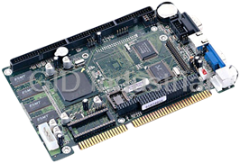


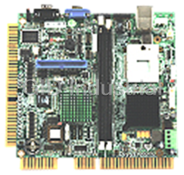
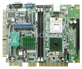
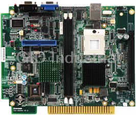


What they say about us
FANTASTIC RESOURCE
One of our top priorities is maintaining our business with precision, and we are constantly looking for affiliates that can help us achieve our goal. With the aid of GID Industrial, our obsolete product management has never been more efficient. They have been a great resource to our company, and have quickly become a go-to supplier on our list!
Bucher Emhart Glass
EXCELLENT SERVICE
With our strict fundamentals and high expectations, we were surprised when we came across GID Industrial and their competitive pricing. When we approached them with our issue, they were incredibly confident in being able to provide us with a seamless solution at the best price for us. GID Industrial quickly understood our needs and provided us with excellent service, as well as fully tested product to ensure what we received would be the right fit for our company.
Fuji
HARD TO FIND A BETTER PROVIDER
Our company provides services to aid in the manufacture of technological products, such as semiconductors and flat panel displays, and often searching for distributors of obsolete product we require can waste time and money. Finding GID Industrial proved to be a great asset to our company, with cost effective solutions and superior knowledge on all of their materials, it’d be hard to find a better provider of obsolete or hard to find products.
Applied Materials
CONSISTENTLY DELIVERS QUALITY SOLUTIONS
Over the years, the equipment used in our company becomes discontinued, but they’re still of great use to us and our customers. Once these products are no longer available through the manufacturer, finding a reliable, quick supplier is a necessity, and luckily for us, GID Industrial has provided the most trustworthy, quality solutions to our obsolete component needs.
Nidec Vamco
TERRIFIC RESOURCE
This company has been a terrific help to us (I work for Trican Well Service) in sourcing the Micron Ram Memory we needed for our Siemens computers. Great service! And great pricing! I know when the product is shipping and when it will arrive, all the way through the ordering process.
Trican Well Service
GO TO SOURCE
When I can't find an obsolete part, I first call GID and they'll come up with my parts every time. Great customer service and follow up as well. Scott emails me from time to time to touch base and see if we're having trouble finding something.....which is often with our 25 yr old equipment.
ConAgra Foods