

 Manufacturers
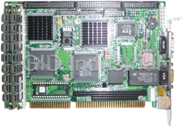
AAEON SBC-552

Description
Half-Size ISA Pentium CPU Card
Part Number
SBC-552
Price
Request Quote
Manufacturer
AAEON
Lead Time
Request Quote
Category
Single Board Computers
Specifications
System Chipset
SiS 5598
Form Factor
Half-Size ISA
Video Chipset
SiS 5598
Datasheet

Extracted Text
SBC-551/552
Half-Size PISA/ISA Pentium CPU Card
FCC STATEMENT
THIS DEVICE COMPLIES WITH PART 15 FCC RULES. OPERA-
TION IS SUBJECT TO THE FOLLOWING TWO CONDITIONS:
(1) THIS DEVICE MAY NOT CAUSE HARMFUL INTERFER-
ENCE. (2) THIS DEVICE MUST ACCEPT ANY INTERFERENCE
RECEIVED INCLUDING INTERFERENCE THAT MAY CAUSE
UNDESIRED OPERATION.
THIS EQUIPMENT HAS BEEN TESTED AND FOUND TO
COMPLY WITH THE LIMITS FOR A CLASS "A" DIGITAL
DEVICE, PURSUANT TO PART 15 OF THE FCC RULES.
THESE LIMITS ARE DESIGNED TO PROVIDE REASON-
ABLE PROTECTION AGAINTST HARMFUL INTERFER-
ENCE WHEN THE EQUIPMENT IS OPERATED IN A
COMMERCIAL ENVIRONMENT. THIS EQUIPMENT GENER-
ATES, USES, AND CAN RADIATE RADIO FREQUENCY
ENERGY AND, IF NOT INSTATLLED AND USED IN ACCOR-
DANCE WITH THE INSTRUCTION MANUAL, MAY CAUSE
HARMFUL INTERFERENCE TO RADIO COMMUNICA-
TIONS. OPERATION OF THIS EQUIPMENT IN A RESIDEN-
TIAL AREA IS LIKELY TO CAUSE HARMFUL INTERFER-
ENCE IN WHICH CASE THE USER WILL BE REQUIRED
TO CORRECT THE INTERFERENCE AT HIS OWN EX-
PENSE.
Copyright Notice
This document is copyrighted, 1998, by AAEON Technology Inc.
All rights are reserved. AAEON Technology Inc. reserves the right
to make improvements to the products described in this manual at
any time without notice.
No part of this manual may be reproduced, copied, translated or
transmitted in any form or by any means without the prior written
permission of AAEON Technology Inc. Information provided in
this manual is intended to be accurate and reliable. However,
AAEON Technology Inc. assumes no responsibility for its use, nor
for any infringements upon the rights of third parties which may
result from its use.
Acknowledgements
AMD is a trademark of Advanced Micro Devices, Inc.
Award BIOS is a trademark of Award Software International, Inc.
AutoCAD and AutoShade are trademarks of Autodesk, Inc.
CHIPS Logotype is a registered trademark. Chips 65554 is a
trademark of Chip and Technologies, Inc.
Cyrix is a trademark of Cyrix Corporation.
IBM, PC/AT, PS/2, and VGA are trademarks of International
Business Machines Corporation.
Intel and Pentium are trademarks of Intel Corporation.
Lotus 1-2-3 and Symphony are trademarks of Lotus Development
Corp.
®
Microsoft Windows and MS-DOS are registered trademarks of
Microsoft Corp.
SiS is a trademark of Silicon Integrated System Corp.
SMC is a trademark of Standard Microsystems Corporation.
UMC is a trademark of United Microelectronics Corporation.
®
VESA is a registered trademark of Video Electronics Standards
Association.
All other product names or trademarks are properties of their
respective owners.
Part No. 2007551000 SBC-551/552 1st Edition
Printed in Taiwan Aug 1998
Packing list
Before you begin installing your card, please make sure that the
following materials have been shipped:
• 1 SBC-551/552 CPU Card
• 1 User Manual (this book)
• 1 Hard disk drive (IDE) interface cable (44 pin)
• 1 Floppy disk drive interface cable (34 pin)
• 1 6-pin mini-DIN dual outlet adapter for keyboard and PS/2
mouse
• 1 Parallel port adapter (26 pin) and COM1 adapter (9 pin) kit
• 4 Utility disks with SiS 5598 utility programs and drivers
• 1 bag of screws and miscellaneous parts
If any of these items are missing or damaged, contact your distribu-
tor or sales representative immediately.
Notice
Dear Customer,
Thank you for purchasing the SBC-551/552 board. The user
manual is designed to help you to get the most out of the SBC-551/
552, please read it thoroughly before you install and use the board.
This product that you have purchased comes with a one-year
limited warranty; AAEON will not be responsible for any misuse of
the product. Therefore, we strongly urge that user first read the
manual before using the product.
To receive the lastest version of the user manual, please visit our
Web site at:
Taiwan: www.aaeon.com.tw
U.S.A : www.aaeon.com
Contents
Chapter 1: General Information .......................1
Introduction ........................................................................... 2
Features.................................................................................. 3
Specifications ......................................................................... 4
Board layout (SBC-551)(PISA Slot) ................................... 6
Board layout (SBC-552)(ISA Slot)...................................... 7
Card dimensions.................................................................... 8
Chapter 2: Installation .......................................9
Jumpers and connectors .................................................... 10
Locating jumpers, connectors and sockets .................... 11
Setting jumpers ................................................................... 12
Safety precautions ............................................................... 13
Installing the CPU............................................................... 14
SIMM installation/removal................................................ 15
Hardware reset (JP1) ......................................................... 16
Thermal alarm LED (JP2) ................................................. 16
Internal SVGA setting (JP3) ............................................. 16
Clear CMOS data (JP4) ..................................................... 17
CPU type select (JP5) ........................................................ 17
CPU external clock selection (JP7)................................. 18
CPU clock ratio (JP8)......................................................... 19
Vcore voltage selection (SW1).......................................... 20
DOC address (JP9)............................................................. 21
RS-232/422/485 selection (JP10) ..................................... 20
PS/mouse enable/disable (JP11) ....................................... 22
CPU jumper setting example ............................................ 23
Hard disk LED connector (CN1) ..................................... 30
IDE hard drive connector (CN2) ...................................... 28
Floppy drive connector (CN3) .......................................... 30
Parallel (printer) port connector (CN4)........................... 31
Fan connector (CN5) .......................................................... 32
USB connector (CN6)......................................................... 32
Serial port connectors (CN10, CN7)................................ 33
RS-232 connector (CN10) ......................................................33
RS-232/422/485 connector (CN7) ........................................... 34
Reserved IR connector (CN8).......................................... 35
Power connector (CN9)...................................................... 35
VGA connector (CN11) ...................................................... 36
KB/PS2 mouse connector (CN12).................................... 37
DiskOnChip socket (U15) ................................................. 38
Chapter 3: Award BIOS Setup ..........................41
System test and initialization ............................................. 42
System configuration verification ............................................ 42
AWARD BIOS setup............................................................43
Entering setup .......................................................................... 43
Standard CMOS setup ....................................................... 44
BIOS features setup ........................................................... 46
CHIPSET features setup ................................................... 50
Power management setup.................................................. 53
PnP/PCI configuration setup ............................................. 59
Load BIOS defaults/Load SETUP defaults ..................... 62
Integrated Peripherals Setup ............................................ 63
Supervisor/user password setting .................................... 67
IDE HDD auto detection ................................................... 69
HDD low level format utility.............................................. 71
Save & exit setup................................................................ 72
Exit without saving ............................................................. 73
Chapter 4: SiS 5598 VGA Drivers ......................75
System requirements.......................................................... 76
Windows 95 .......................................................................... 76
Windows 95 (display driver installation) .................................. 76
Selecting resolution, color depth, and refresh rate ................... 77
Windows 3 3 3 3 3 . . . . .x ........................................................................ 78
Installing ..................................................................................78
Graphics setup ......................................................................... 78
Power saving setup in Windows 3.x........................................79
NT 3.5X................................................................................. 79
Windows NT 3.5x display divers installation ........................... 79
Selecting resolution and color depth ........................................ 80
NT 4.0 ................................................................................... 80
windows NT 4.0 display drivers installation ............................ 80
Selecting resolution and color depth ........................................ 81
DOS ....................................................................................... 82
VGA utility .............................................................................. 82
Video uode uetting ................................................................... 82
Frame rate setting ...................................................................82
Power saving setting ...............................................................82
Appendix A: Programming the Watchdog
Timer.............................................83
Programming the watchdog timer .................................... 84
How to program the watchdog timer ......................................84
Demo program ........................................................................85
1
General
Information
This chapter provides background
information for the SBC-551/552.
Sections include:
• Card specifications
• Board layout
Chapter 1 General Information 1
CHAPTER
Introduction
The SBC-551/552 is an all-in-one Single Board Computer (SBC)
capable of handling the Intel Pentium P54C, P55C (MMX), AMD
K6, as well as the Cyrix 6x86 (M1) and 6x86MX (M2) CPUs.
Reliability, performance, flexibility, and adequate expansion
capabilities are essential qualities for SBCs and their embedded
applications and the SBC-551/552 provides all of these.
The Smart Temperature Control technology (LM75 chip) monitors
the CPU temperature and automatically slows down the CPU
frequency when the CPU temperature exceeds a specified safe
range, helping your system recover from abnormal temperature
fluctuations.
The SBC-551/552 supports the M-Systems DiskOnChip 2000
(optional) which is a new generation of high performance single-
chip Flash Disk. It provides a Flash Disk (as a BIOS expansion)
which doesn't require any bus, slots, or connectors. It is also the
optimal solution for Single Board Computers because of its small
size, easy integration, plug-and-play functionality, and its low
power consumption. The DiskOnChip is available in capacities
from 2MB to 72MB and fits in a standard 32-pin DIP socket.
The SBC-551/552 also includes a high speed, local bus IDE
controller which supports (through ATA PIO) mode 3 and mode 4
hard disks, Ultra DMA/33 (data transfer rates up to 33MB/sec) and
up to 2 IDE devices.
Onboard features include one high speed RS-232 serial port, one
RS-232/422/485 serial port with 16C550 UARTs, one bidirectional
SPP/EPP/ECP parallel port, and a floppy drive controller. In
addition to the 486's 16 KB of onchip cache memory, the SBC-551/
552 includes an extra 512 KB of pipeline-burst L2 cache memery.
If program execution is halted by a program bug or EMI, the board's
watchdog timer can automatically reset the CPU or generate an
interrupt. This ensures reliability in unmanned or standalone
systems.
2 SBC-551/552 User Manual
The SBC-551/552 provides two 72-pin SIMM (Single In-line
Memory Module) sockets for intalling onboard system DRAM.
These sockets give you the flexibility to configure your system
from 4 MB to 128 MB of DRAM using the most economical
combination of SIMMs.
Features
• Supports Pentium P54C/P55C (MMX), AMD K6, and Cyrix M1/M2
CPUs
• Half-size PISA bus CPU Card for SBC-551, and half-size ISA bus CPU
Card for SBC-552
• Equipped with a switching power module supporting up to 10 Ampere
CPU power consumption
• DiskOnChip (SSD) up to 72MB
• SiS 5598 chipset: XGA controller integrated
• Bus Master IDE and Ultra DMA/33 supported
• LM75 supports CPU temperature & fan monitoring
Chapter 1 General Information 3
Specifications
CPU: Intel Pentium MMX 166~233MHz, AMD-K6/200~300AFR, Cyrix /
IBM/6x86MX-PR166~266GP and IDT winchip C6 180~225MHz
BIOS: Award FLASH BIOS
Chipset: SiS 5598
Bus interface: PISA Bus for SBC-551, ISA Bus for SBC-552
Level 2 Cache: Onboard 512KB pipeline-burst L2 cache.
System memory: Two 72-pin SIMM sockets. Supports up to 128MB
DRAM.
DMA channels: 7
Interrupt levels: 15
Battery: Lithium battery for data retention of up to 10 years.
Enhanced IDE: Supports up to two IDE devices. BIOS auto-detect,
supports PIO mode 4 and Bus Master. Also supports multi-word DMA
and Ultra DMA/33.
FDD interface: Supports up to two floppy disk drives.
Parallel port: Configured to LPT1, LPT2, LPT3, or disabled. Supports
SPP, ECP, and EPP.
Serial ports: One RS-232 and one RS-232/422/485 serial port. Ports can be
configured as COM1, COM2, COM3, COM4, or disabled individually. Two
16C550 serial UARTs.
IrDA interface: One IrDA connector reserved for future use.
Keyboard/mouse connector: 6-pin mini-DIN connector supports standard
PC/AT Keyboard and PS/2 mouse.
USB connectors: One USB connector onboard. (Support two USB
channels)
Watchdog Timer: Can generate a system reset, IRQ15, or NMI. Software
selectable time out interval (2 sec ~ 128 min, 1 sec/step).
Power management: I/O peripheral devices support power saving and
doze/standby/suspend modes. APM 1.2 compliant
VGA controller: SiS 5598
4 SBC-551/552 User Manual
Display memory: Supports shared system memory up to 4MB.
Display type: Supports a CRT display.
Resolution: Support up to 1024 x 768 @ 16.7M colors.
SSD interface: One 32-pin DIP socket supports the M-Systems DiskOn-
Chip 2000 series, memory capacity from 2MB to 72MB.
CPU thermal: LM75 supports CPU temperature & fan monitoring.
Power supply voltage: +5V (4.75V to 5.25V)
+12V (11.4V to 12.6V)
Power Requirement:
Bare Board: +5V @ 1.5A
Pentium MMX-200: +5V @ 6A
AMD K6-233: +5V @ 10A
° ° ° °
Operating temperature: 32 F to 140 F (0 C to 60 C)
Board size: 7.3" (L) x 4.8" (W) (185 mm x 122 mm)
Board weight: 0.23 kg
Chapter 1 General Information 5
Board layout (SBC-551)(PISA Slot)
6 SBC-551/552 User Manual
Winbond
DiskOnChip
BAT
14.318
SIS
5598
CPU
SOCKET
iTE
IT8661
Board layout (SBC-552)(ISA Slot)
Chapter 1 General Information 7
Winbond
DiskOnChip
BAT
14.318
SIS
5598
CPU
SOCKET
iTE
IT8661
Card dimensions
185.00
178.00
98.50 19.50
122.00
8 SBC-551/552 User Manual
D4x4
2
Installation
This chapter explains setup procedures
for the SBC-551/552 hardware, including
instructions on setting jumpers and
connecting peripherals, switches and
indicators. Be sure to read all safety
precautions before you begin the installa-
tion procedure.
Chapter 2 Installation 9
CHAPTER
Jumpers and connectors
Connectors on the board link to external devices such as hard disk
drives, keyboard, or floppy drives. In addition, the board has a
number of jumpers that allow you to configure your system to suit
your applications.
The tables below lists the function of each of the board jumpers
and connectors:
Jumper Label Function
JP1 Hardware reset
JP2 Thermal alarm LED
JP3 Int VAG setting
JP4 Clear CMOS
JP5 Vio voltage setting
JP7 CPU clock setting
JP8 CPU frequency ratio
JP9 DOC address setting
JP10 RS-232/422/485 select
JP11 PS/2 mouse setting
SW1 CPU voltage setting
Connector Label Function
CN1 IDE LED connector
CN2 HDD connector
CN3 Floppy drive connector
CN4 Parallel (Printer) connector
CN5 Fan connector
CN6 USB connector
CN7 COM2 connector
CN8 Reserved IR connector
CN9 Power connector
CN10 COM1 connector
CN11 VGA connector
CN12 KB/PS2 mouse connector
10 SBC-551/552 User Manual
Locating jumpers, connectors, and
sockets
Power
COM 1(CN10) VGA(CN11) Keyboard/
connector
connector Port Mouse Port (CN12)
COM 2 (CN7)
CN8
connector
RS-232/422/485
select (JP10)
Fan connector
CN6
(CN5)
Socket for
DiskOnChip
Parallel Port
connector
(CN4)
JP9
FDD
Award
connector
Flash BIOS
(CN3)
JP8
JP7
SW1
JP11 PS/2 mouse
JP5
Enable/Disable
JP4
SiS 5598
Chipset
PISA Bus
(PCI+ISA)
IDE
connector
(CN2)
Reset SW
(JP1)
Up to
128MB DRAM
IDE LED
JP2 JP3
(CN1)
Chapter 2 Installation 11
Winbond
DiskOnChip
BAT
14.318
SIS
5598
CPU
SOCKET
iTE
IT8661
Setting jumpers
By setting the jumpers, you can configure your card to match the
needs of your specific applications. A jumper is the simplest kind
of electric switch. It consists of two metal pins and a small metal
clip (often protected by a plastic cover) that slides over the pins to
connect them. To close a jumper you connect the pins with the
clip. To "open" a jumper you remove the clip. Sometimes a jumper
will have three pins, labeled 1, 2, and 3. In this case you would
connect either pins 1 and 2 or 2 and 3.
3
2
1
Open Closed Closed 2-3
The jumper settings are schematically depicted in this manual as
follows:
1 2 3
Open Closed Closed 2-3
A pair of needle-nose pliers may be helpful when working with
jumpers.
If you have any doubt about the best hardware configuration for
your applications, contact your local distributor or sales represen-
tative before you make any changes.
12 SBC-551/552 User Manual
Safety precautions
Warning! Always completely disconnect the power cord from
your chassis whenever you are working on it. Do
not make connections while the power is on
because sensitive electronic components can be
damaged by the sudden rush of power. Only
experienced electronics personnel should open
the PC chassis.
Caution! Always ground yourself to remove any static
charge before touching the CPU card. Modern
electronic devices are very sensitive to static
electric charges. Use a grounding wrist strap at all
times. Place all electronic components on a
static-dissipative surface or in a static-shielded
bag when they are not in the chassis.
Conflicts! The VGA controller of SBC-551/552 uses IDSEL
No. 31, which is the same as that of the first PCI
slot (i.e., "PCI1") on the PCI backplane (PICMG
2.0 standard). Therefore, when the onboard VGA
function is enabled, the first PCI slot on the PCI
backplane cannot have a peripheral card plugged
in otherwise hardware conflicts can result.
Chapter 2 Installation 13
Installing the CPU
The SBC-551/552 CPU card supports most Pentium and its compati-
ble CPUs. The system's performance depends on the CPU you
choose. You can install or upgrade the CPU in the board's PGA
socket by following the procedures outlined below. If your system
has an existing CPU, you need to remove it before installing the
new CPU.
Removing a CPU
1. Disconnect power from the chassis, and unplug all connections
to the CPU card. Then, remove the CPU card from the chassis
by following the instructions in the user manual for your
chassis.
2. Lift the CPU out of the PGA socket. The old chip may be
difficult to remove. You may find spray chip lubricant, designed
for pin-grid-array (PGA) devices, and a chip puller helpful.
These are available at electronics hobbyists' supply stores.
Installing a CPU
To install the CPU, follow the instructions that came with it. If no
documentation was provided, the general procedures for installing
a CPU are outlined below:
1. Lubricate the pins on the CPU with lubricant for PGA devices.
This makes the CPU slide in much easier and greatly reduces
the chance of damaging the pins and other components.
2. Carefully align the CPU so that it is parallel to the socket. Make
sure that the notch on the corner of the CPU matches the notch
on the inside of the socket.
3. Gently push the CPU into the socket. There will probably be a
small gap between the CPU and the socket even when it is fully
seated. Do not use execessive force !
When you install a new CPU, you may have to adjust other
settings on the board, such as CPU type, CPU clock, and PCI
speed, in order to accommodate it. Make sure that the settings are
correct for your CPU. Improper settings may damage the CPU.
14 SBC-551/552 User Manual
Installing DRAM (SIMM1, SIMM2)
The SBC-551/552 provides two 72-pin SIMM (Single In-line
Memory Module) sockets. The SIMM supports either Fast Page
Mode (FPM) or Extended Data Output (EDO) DRAM with a speed
of at least 70 ns. Depending on the combination of modules you
use, you can install from 4 MB to 128 MB of RAM.
Installing SIMMs
NOTE 1: Pentium or compatible processors adopt 64 bit data bus.
Since 72-pin SIMM can only provide 32 bit data bus
width, two SIMM modules are required as one memory
bank, and both SIMMs must be the same size and type.
1. Ensure that all power sources are disconnected.
2. Slip the memory module into the socket at a 45 degree angle.
3. Push the module toward the vertical posts at both ends of the
socket until the module is upright and the retaining clips at both
ends of the module click into place. When positioned correctly,
the pins on top of the vertical posts should correspond to the
circular holes on the ends of the module.
4. Repeat steps 2 and 3 for each module you install.
NOTE 2: Do not insert any SIMM module that contains more
than 24 memory chips. SIMMs contain more than 24
chips exceed the driving capability of new generation
chipsets.
Chapter 2 Installation 15
Hardware reset (JP1)
You can connect an external switch to easily reset your computer.
The following table shows the pin assignments.
Hardware reset (JP1)
Normal Reset
1 2 1 2
Thermal alarm LED (JP2)
The thermal alarm connector (JP2) allows the user to connect an
alarm indicator LED on the case.
Thermal alarm LED (JP2)
Pin Signal
1 3.3V (Alarm out)
2 GND
Internal SVGA setting (JP3)
The SBC-551/552 core logic chipset is SiS 5598 which has built-in
VGA adapter. You can disable the internal VGA functions by
setting JP3.
Internal SVGA setting (JP3)
Enable* Disable
1 2
1 2
3 4
3 4
5 6
5 6
*default
16 SBC-551/552 User Manual
Clear CMOS (JP4)
You can connect an external jumper cap or switch to clear CMOS.
Clear CMOS procedure:
1. Disconnect all power source.
2. Move JP4 from 1-2 to 2-3 for few seconds.
3. Move JP4 back to 1-2.
Clear CMOS (JP4)
Normal* Clear CMOS
1 2 3 1 2 3
*default
CPU type select (JP5)
JP5 must be set to match the CPU type between Dual-Voltage ( e.g.,
P55C ) and Single-Voltage ( e.g., P54C ) type CPU. The chart below
shows the proper jumper setting for their respective CPU type.
CPU type select (JP5)
Dual-Voltage* Single-Voltage
JP5
1 2 3
1 2 3
* default
WARNING: Improper setting could damage the CPU.
Chapter 2 Installation 17
CPU clock setting (JP7)
JP7 is used to sychronize the system clock with the CPU type. You
may need to adjust the CPU clock according to the base CPU
speed.
CPU clock setting (JP7)
50 MHz 55MHz 60MHz
2 4 6 2 4 6 2 4 6
1 3 5 1 3 5 1 3 5
66.6MHz*
2 4 6
1 3 5
*default
18 SBC-551/552 User Manual
CPU frequency ratio (JP8)
JP8 must be set to match the CPU clock ratio. The chart below
show the proper jumper settings for P54C, P55C, AMD-K6, and
Cyrix 6x86 MX (M2), and their respective clock ratios.
CPU frequency Ratio (JP8)
JP6 P54C P55C AMD-K6 Cyrix 6x86MX
2 4 6
1.5 3.5 3.5 3.5
3
1 5
2 4 6
2.0 2.0 2.0 2.0
3
1 5
2 4 6
* 3.0 3.0 3.0 3.0
3 5
1
2 4 6
2.5 2.5 2.5 2.5
1 3
5
2 4 6
- - 5.5 5.5
1 3 5
4 6 - - 4.0 4.0
2
1 3
5
- - 5.0 5.0
2 4 6
1 3 5
2 4 6
- - 4.5 4.5
1 3 5
* default setting
Chapter 2 Installation 19
CPU voltage setting (SW1)
CPU core voltage can be set by SW1 to reduce power consumption
and heat.
CPU voltage setting (SW1)
2.0V 2.1V 2.2V
28 4 6 2468 2468
3 3
3 1 57 1 57
1 57
2.3V 2.4V 2.5V
2468 2468
2846
357 357 3
1 1 175
2.6V 2.7V 2.8V*
468 468
2 2846 2
3 3 3
1 57 1 57 1 57
2.9V 3.0V 3.1V
2468
2468 2468
3
1 57
1357 1357
3.2V 3.3V 3.4V
46 46 46
28 28 28
3 3
1 57 1357 1 57
3.5V
46
28
3 7
1 5
*default
WARNING: Improper setting could damage the CPU!
20 SBC-551/552 User Manual
DOC address setting (JP9)
The DiskOnChip (DOC) 2000 is a flash disk and occupies an 8 KB
window in the upper memory address range of CC000 to DC000.
You should ensure this does not conflict with any other devices'
memory addresses. JP9 controls the starting memory address of
the flash disk. For more information about the DOC chip, refer to
the "DiskOnChip Socket (U15)" section in this chapter .
DiskOnChip 2000 memory address
Memory address (HEX) JP9
CC000 D0000 (Default)
2 4 6 2 4 6
*
1 3 5 1 3 5
D4000 D8000
2 4 6 2 4 6
1 3 5 1 3 5
DC000
2 4 6
1 3 5
*default
* Before installation, refer to page 38, please.
WARNING : These addresses might conflict with the ROM BIOS
of other peripheral boards. Please select appropri
ate memory address to avoid memory conflicts.
Chapter 2 Installation 21
RS-232/422/485 select (JP10)
The SBC-551/552 offers two serial ports. One RS-232 COM1 (CN10)
and one RS-232/422/485 COM2 (CN7). The mode of CN7 can be
selected via JP10.
The following charts show the available options:
RS-232/422/485 select (JP10)
RS-232* RS-422 RS-485
1 2 1 2 1 2
3 4 3 4 3 4
5 6 5 6 5 6
* default
PS/2 mouse enable/disable (JP11)
PS/2 mouse enable/disable (JP11)
1-2 (Enable) 2-3 (Disable)
1 2 3
1 2 3
22 SBC-551/552 User Manual
CPU Jumper Setting Example
CPU Clock Clock JP8 JP7 SW1 JP5
Int/Ext(MHz) Ratio (Ratio) (External) (Vcore) (Dual/Single)
2 4 6 2 4 6
2 4 6 8
Intel Pentium 200/66 3
P54C
1 2 3
1 3 5 1 3 5
1 3 5 7
(3.3V)
2 4 6
2 4 6 2 4 6 8
Intel Pentium 166/66 2.5
P54C
1 2 3
1 3 5
1 3 5 1 3 5 7
(3.3V)
2 4 6
2 4 6 2 4 6 8
Intel Pentium 75/50 1.5
P54C
1 2 3
1 3 5
1 3 5 1 3 5 7
(3.3V)
2 4 6 2 4 6 8
2 4 6
Intel Pentium 90/60 1.5
P54C
1 2 3
1 3 5 1 3 5 7
(3.3V) 1 3 5
2 4 6 8
2 4 6
2 4 6
Intel Pentium 100/66 1.5
P54C
1 2 3
1 3 5 7
1 3 5
(3.3V)
1 3 5
2 4 6 8
2 4 6 2 4 6
Intel Pentium 120/60 2.0
P54C
1 2 3
1 3 5 7
1 3 5 1 3 5
(3.3V)
2 4 6 2 4 6 8
2 4 6
Intel Pentium 133/66 2.0
P54C
1 2 3
1 3 5
1 3 5 7
(3.3V) 1 3 5
2 4 6
2 4 6 2 4 6 8
Intel Pentium 150/60 2.5
P54C
1 2 3
1 3 5
1 3 5 1 3 5 7
(3.3V)
Chapter 2 Installation 23
CPU Jumper Setting Example
CPU Clock Clock JP8 JP7 SW1 JP5
Int/Ext(MHz) Ratio (Ratio) (External) (Vcore) (Dual/Single)
2 4 6 2 4 6
Intel Pentium 233/66 3.5 2 4 6 8
P55C PP/MT
1 2 3
(2.8V) 1 3 5 1 3 5
1 3 5 7
2 4 6
2 4 6
Intel Pentium 200/66 3.0 2 4 6 8
P55C PP/MT
1 2 3
(2.8V) 1 3 5 1 3 5
1 3 5 7
24 SBC-551/552 User Manual
CPU Jumper Setting Example
CPU Clock Clock JP8 JP7 SW1 JP5
Int/Ext(MHz) Ratio (Ratio) (External) (Vcore) (Dual/Single)
2 4 6 2 4 6
AMD K5 75/50 1.5 2 4 6 8
PR-75
1 2 3
1 3 5 1 3 5
(3.54V) 1 3 5 7
2 4 6 2 4 6
2 4 6 8
AMD K5 90/60 1.5
PR-90
1 2 3
1 3 5 1 3 5 1 3 5 7
(3.54V)
2 4 6 8
2 4 6 2 4 6
AMD K5 100/66 1.5
PR-100
1 2 3
1 3 5 7
(3.54V) 1 3 5 1 3 5
2 4 6 8
2 4 6
AMD K5 90/60 1.5 2 4 6
PR-120
1 2 3
1 3 5 7
(3.54V) 1 3 5
1 3 5
2 4 6 2 4 6 2 4 6 8
AMD K5 100/66 1.5
PR-133
1 2 3
(3.54V) 1 3 5 1 3 5 1 3 5 7
Chapter 2 Installation 25
CPU Jumper Setting Example
CPU Clock Clock JP8 JP7 SW1 JP5
Int/Ext(MHz) Ratio (Ratio) (External) (Vcore) (Dual/Single)
2 4 6 2 4 6 2 4 6 8
AMD K6 166/66 2.5
PR2-166
1 2 3
(2.9V) 1 3 5 1 3 5
1 3 5 7
2 4 6 8
2 4 6
2 4 6
AMD K6 166/66 3.0
PR2-200
1 2 3
1 3 5
(2.9V) 1 3 5 1 3 5 7
2 4 6 8
2 4 6
2 4 6
AMD K6 233/66 3.5
PR2-233
1 2 3
(3.2V) 1 3 5 1 3 5
1 3 5 7
2 4 6 8
2 4 6 2 4 6
AMD K6 266/66 4.0
PR2-266
1 2 3
(2.0V) 1 3 5 1 3 5
1 3 5 7
26 SBC-551/552 User Manual
CPU Jumper Setting Example
CPU Clock Clock JP8 JP7 SW1 JP5
Int/Ext (MHz)Ratio (Ratio) (External) (Vcore) (VIO)
2 4 6 8
2 4 6 2 4 6
Cyrix 6x86M2 133/66 2.0
MX-PR166
1 2 3
1 3 5 1 3 5
(2.9V) 1 3 5 7
2 4 6 8
2 4 6
2 4 6
Cyrix 6x86M2 150/60 2.5
MX-PR166
1 2 3
1 3 5
(2.9V) 1 3 5 1 3 5 7
2 4 6 8
2 4 6 2 4 6
Cyrix 6x86M2 166/66 2.5
MX-PR200
1 2 3
(2.9V) 1 3 5 1 3 5 1 3 5 7
2 4 6 8
2 4 6 2 4 6
Cyrix 6x86M2 200/66 3.0
MX-PR233
1 2 3
(2.9V) 1 3 5 1 3 5
1 3 5 7
2 4 6 2 4 6 8
2 4 6
Cyrix 6x86M2 233/66 3.5
MX-PR266
1 2 3
1 3 5
(2.9V) 1 3 5
1 3 5 7
Chapter 2 Installation 27
IDE LED connector (CN1)
You can connect an LED to indicate that an IDE device is in use.
The pin assignments of CN1 are as follows:
IDE LED connector (CN1)
Pin Signal
1 -R/W IDE
2 VCC
IDE hard drive connector (CN2)
You can attach two Enhanced Integrated Device Electronics hard
disk drives to the SBC-551/552's internal controller. The card comes
with a 40-pin flat piggyback cable. This cable has three identical
40-pin flat-cable connectors.
Connecting the hard drive
Connecting drives is done in a daisy-chain fashion and requires
one of two cables, depending on the drive size. 1.8" and 2.5" drives
need a 1 x 44-pin to 2 x 44-pin flat-cable connector for CN6. 3.5"
drives use a 1 x 40-pin to 2 x 40-pin connector for CN5.
Wire number 1 on the cable is marked as red or blue, and the other
wires are gray.
1. Connect one end of the cable to CN5 or CN6. Make sure that
the red (or blue) wire corresponds to pin 1 on the connector,
which is labeled on the board (on the right side).
2. Plug the other end of the cable to the Enhanced IDE hard drive,
with pin 1 on the cable corresponding to pin 1 on the hard
drive. (See your hard drive's documentation for the location of
the connector.)
28 SBC-551/552 User Manual
Connect a second drive as described above.
Unlike floppy drives, IDE hard drives can connect to either end of
the cable. If you install two drives, you will need to set one as the
master and one as the slave by using jumpers on the drives. If you
install just one drive, set it as the master.
Pin assignments
The following table lists the pin numbers and their respective
signals:
IDE Connector (CN2)
Pin Signal Pin Signal
1 Reset 2 GND
3D7 4 D8
5D6 6 D9
7 D5 8 D10
9D4 10 D11
11 D3 12 D12
13 D2 14 D13
15 D1 16 D14
17 D0 18 D15
19 GND 20 N.C.
21 N.C. 22 GND
23 IOW 24 GND
25 IOR 26 GND
27 IORDY 28 BALE
29 N.C. 30 GND
31 IRQ 14 32 -I/O CS16
33 A1 34 N.C.
35 A0 36 A2
37 CS0 38 CS1
39 -ACT 40 GND
Chapter 2 Installation 29
Floppy drive connector (CN3)
You can attach up to two floppy disks to the SBC-551/552 onboard
controller. You can use any combination of 5¼" (360 KB and 1.2
MB) and/or 3½" (720 KB, 1.44 MB, and 2.88 MB) drives.
A 34-pin daisy-chain drive connector cable is required for a dual-
drive system. On one end of the cable is a 34-pin flat-cable
connector. On the other end are two sets of floppy disk drive
connectors. Each set consists of a 34-pin flat-cable connector
(usually used for 3½" drives) and a printed-circuit board connector
(usually used for 5¼" drives).
Connecting the floppy drive
1. Plug the 34-pin flat-cable connector into CN3. Make sure that
the red wire corresponds to pin one on the connector.
2. Attach the appropriate connector on the other end of the cable
to the floppy drive(s). You can use only one connector in the
set. The set on the end (after the twist in the cable) connects to
the A: drive. The set in the middle connects to the B: drive.
Pin assignments
The following table lists the pin assignments for the CN3 connec-
tor:
FLOPPY drive connector (CN3)
Pin Signal Pin Signal
1~33 (odd)GND 2 High density
4, 6 Unused 8 Index
10 Motor enable A 12 Driver select B
14 Driver select A 16 Motor enable B
18 Direction 20 Step pulse
22 Write data 24 Write enable
26 Track 0 28 Write protect
30 Read data 32 Select head
34 Disk change
30 SBC-551/552 User Manual
Parallel (printer) port connector
(CN4)
Normally, the parallel port is used to connect the card to a printer.
The SBC-551/552 includes an onboard parallel port, accessed
through CN4, a 26-pin flat-cable connector. You need an adapter
cable if you use a traditional DB-25 connector. The cable has a 26-
pin connector on one end and a DB-25 connector on the other.
Mounted on a retaining bracket.
Parallel port IRQ
The SBC-551/552 supports one parallel port. The port is designat-
ed as LPT1 and can be disabled or changed to LPT2 or LPT3 in the
system BIOS setup.
Pin assignments
Parallel (printer) port connector (CN4)
Pin Signal Pin Signal
1 Strobe 2 Data 0
3 Data 1 4 Data 2
5 Data 3 6 Data 4
7 Data 5 8 Data 6
9 Data 7 10 -Acknowledge
11 Busy 12 Paper empty
13 +Select 14 -Auto feed
15 -Error 16 -Init printer
17 -Select input 18~25 GND
Chapter 2 Installation 31
Fan connector (CN5)
The SBC-551/552 provides a connector for CPU cooling fan.
Fan power connector (CN5)
Pin Signal
1 +12 V
2 FAN_ON
3 +5V
USB connector (CN6)
The USB connector supports two universal serial ports. This
connector allows an optional external adaptor and attached cable to
connect external USB devices. If the USB ports are installed, the
USB setting in the CMOS setup should be set to Enabled. The
USB ports also require operating system supporting for USB
devices.
The SBC-551/552 CPU card has one USB Connector ( support two
USB channels), their connection pin assignment is as follows.
USB connector (CN6)
Pin Signal Pin Signal
1 VCC 2 VCC
3 -DATA0 4 -DATA1
5 +DATA0 6 +DATA1
7 GND 8 GND
9NC 10 NC
32 SBC-551/552 User Manual
Serial port connectors (CN10, CN7)
The SBC-551/552 offers one RS-232 and one RS-232/422/485 serial
port. You can select the port address or disabled for each port with
the BIOS Peripheral Setup program.
The card mounting bracket holds COM 1(CN10), the DB-9 serial
port connector for the first port. The connector on the SBC-551/
552 board is and COM 2(CN7) for RS-232/422/485. The following
sections tell how to make connections.
RS-232 connector (CN10)
The following table shows the pin assignments for the card's RS-
232 port:
RS-232 connector (CN10, COM1)
Pin Signal
1 DCD
2RX
3TX
4 DTR
5 GND
6 DSR
7 RTS
8 CTS
9RI
10 NC
Chapter 2 Installation 33
RS-232/422/485 connector (CN7)
RS-232/422/485 connector pin assignment (CN7)
Pin Signal
1 DCD
2 DSR
3RX
4 RTS
5TX
6 CTS
7 DTR
8RI
9 GND
10 NC
11 B485TXD+
12 B485TXD-
13 B422RXD+
14 B422RXD-
34 SBC-551/552 User Manual
Reserved IR connector (CN8)
The onboard IR connector supports an Infrared port module that
enables wireless communication between the computer and other
computers and devices with infrared capability. The port module is
an optional component. If it is installed, you must set the IR
Transfer Mode in the Peripherals section of the CMOS setup utility.
Ir Connector
Pin Function
1 VCC
2 FIR_RX (High Frequency)
3 IR_RX (Low Frequency)
4 GND
5 IR_TX
Power connector (CN9)
In single board computer without passive backplane applications,
you need to connect power directly to the SBC-551/552. This
connector is fully compatible with the standard PC power supply
connector. See the following table for its pin assignments:
Power connector (CN9)
Pin Signal
1 +12V
2 GND
3 GND
4 +5V
Chapter 2 Installation 35
VGA connector (CN11)
The SBC-551/552 CPU card's VGA connector supports mono-
chrome display as well as high resolution color displays. The
following table lists their pin assignments:
VGA connector (CN11)
Pin Signal
1 Red video
2 Green video
3 Blue video
4 Not used
5 GND
6 Red return (GND)
7 Green return (GND)
8 Blue return (GND)
9 Key (no pin)
10 Sync return (GND)
11 Monitor ID (not used)
12 Monitor ID
13 Horizontal sync
14 Vertical sync
15 Not used
36 SBC-551/552 User Manual
KB/PS2 mouse connector (CN12)
The SBC-551/552 board provides one keyboard connectors. There
is a second 6-pin mini-DIN connector (CN12) on the card mounting
bracket. The card comes with an adapter to convert the 6-pin mini-
DIN connector, used for the mouse, to the standard DIN connector
for the keyboard.
KB/PS2 MOUSE
Adaptor for connecting a keyboard and PS/2 Mouse.
Mini-Din 6-Pin connector pin definition
Pin Function
1 KBDATA
2 MDATA
3 GND
4 VCC
5 KBCLK
6 MSCLK
Chapter 2 Installation 37
DiskOnChip socket (U15)
The M-Systems DiskOnChip 2000 (DOC-2000) family of products
provides a single chip solid-state flash disk in a standard 32-pin
DIP package. The DOC-2000 is a small, plug-and-play, solid-state
disk with no moving parts, resulting in a significant reduction in
power consumption and an increase in reliability.
The DOC-2000 family of products is available in capacities ranging
from 2MB up to 72 MB, unformatted. This way, the same socket on
the target platform will not have to be changed. In order to manage
the disk, the DOC-2000 includes the TrueFFS, M-Systems Flash
File System proprietary software. The DOC-2000 package is pin-to-
pin compatible with standard 32-pin EPROM devices.
pin
Description Pin Number Direction Note
Name
A0-A12 Address bus 4-12,23,25-27 Inputs
A13-A16 Address bus 2,3,28,29 Inputs 1
D0-D7 Data bus 13-15,17-21 I/O
CE/ Chip Enable 22 Input
OE /
OE/ Output Enable 24 Input
WE/ Write Enable 31 Input
NC Not connected 1.30 2
VCC Power 32
GND Ground 16
Figure1-MD2200 Pin-out
Note 1: Pins A13 through A16 are not used by
the MD2200. They are kept for socket backward
compatibility with ED 1100 (DiskOnChip 1000)
Note 2: Pins 1 and 30 are not used by the
MD2200
Refer to pages 21 for configuring the DOC address (JP9).
38 SBC-551/552 User Manual
DiskOnChip (DOC) 2000 Installation
When the DOC is installed correctly, a DOC will work like a HDD or
a FDD. To install the DOC on the board, follow the instructions
below:
1. Plug the DOC into the socket. Make sure pin 1 of the DOC is
aligned with pin 1 of the socket.
2. Push the DOC into the socket until it is firmly seated in the
socket.
Caution: the DOC may be permanently damaged if it is installed
incorrectly.
3. Set the jumper for the memory address of the DOC.
Note:
The memory shadow function sometimes will create conflicts with
the memory window. You should disable the memory shadow from
the BIOS SETUP if the DOC cannot be accessed.
Configure DOC as a boot device
To configure a DOC as a boot drive, you should copy the operating
system files into the DOC. The following procedure is an example
of the initialization process.
1. Install a DOC into your system.
2. Insert a bootable floppy disk in drive A: and boot the system.
3. At the DOS prompt, type SYS C: to transfer the DOS system
files to the DOC (assuming the DiskOnChip is installed as drive
C:). Reboot the system.
4. Go to the BIOS Setup Utility by hitting the key. Set the
type of Primary Master or C: Drive as Not Installed.
5. Remove the floppy disk from the drive A: and leave the BIOS
Setup Utility. The system should boot from the DOC.
Chapter 2 Installation 39
40 SBC-551/552 User Manual
3
Award BIOS Setup
This chapter describes how to configure
the BIOS for the SBC-551/552.
Chapter 3 Award BIOS Setup 41
CHAPTER
System test and initialization
These routines test and initialize board hardware. If the routines
encounter an error during the tests, you will either hear a few short
beeps or see an error message on the screen. There are two kinds
of errors: fatal and non-fatal. The system can usually continue the
boot up sequence with non-fatal errors. Non-fatal error messages
usually appear on the screen along with the following instructions:
press immediately. This will
allow you to enter the utility and the utility screen should appear
(below).
R O M P C I / I S A B I O S ( 2 A 5 I I A K 9 )
C M O S S E T U P U T I L I T Y
A W A R D S O F T W A R E , I N C .
STANDARD CMOS SETUP INTEGRATED PERIPHERALS
BIOS FEATURES SETUP SUPERVISER PASSWORD
CHIPSET FEATURES SETUP USER PASSWORD
POWER MANAGEMENT SETUP IDE HDD AUTO DETECTION
PNP/PCI CONFIGURATION HDD LOW LEVEL FORMAT
LOAD BIOS DEFAULTS SAVE & EXIT SETUP
LOAD SETUP DEFAULTS EXIT WITHOUT SAVING
ESC: Quit ���: Select Item
F10:Save & Exit Setup (Shift)F2:Change Color
Time, Date, Hard Disk Type.....
Setup Utility Initial Screen
Award’s BIOS ROM has a built-in setup utility that allows users to
modify the basic system configuration. This type of information is
stored in a battery-backed CMOS RAM so that the information is
retained when the power is turned off.
Many fields in the setup screens have on-line help descriptions
available: press F1 to access the help.
Chapter 3 Award BIOS Setup 43
Standard CMOS setup
R O M P C I / I S A B I O S ( 2 A 5 I I A K 9 )
C M O S S E T U P U T I L I T Y
A W A R D S O F T W A R E , I N C .
STANDARD CMOS SETUP INTEGRATED PERIPHERALS
BIOS FEATURES SETUP SUPERVISER PASSWORD
CHIPSET FEATURES SETUP USER PASSSWORD
POWER MANAGEMENT SETUP IDE HDD AUTO DETECTION
PNP/PCI CONFIGURATION HDD LOW LEVEL FORMAT
LOAD BIOS DEFAULTS SAVE & EXIT SETUP
LOAD SETUP DEFAULTS EXIT WITHOUT SAVING
ESC: Quit ���: Select Item
F10:Save & Exit Setup (Shift)F2:Change Color
Time, Date, Hard Disk Type ....
CMOS setup screen
When you choose the STANDARD CMOS SETUP option from the
INITIAL SETUP SCREEN menu, the screen below is displayed.
This standard setup menu allows users to configure system
components such as the date, time, hard disk drive, floppy drive,
display, and memory. Online help for each field can be accessed by
pressing F1.
44 SBC-551/552 User Manual
R O M P C I / I S A B I O S ( 2 A 5 I I A K 9 )
S T A N D A R D C M O S S E T U P
A W A R D S O F T W A R E , I N C .
Date (mm:dd:yy) : Fri, Aug 16, 1998
Time (hh:mm:ss) : 8:20:23
HARD DISKS CYLS HEAD PRECOMP LANDZ SECTOR MODE
Drive C: Auto (0b) : 0 0 0 0 0 AUTO
Drive D: Auto (0b) : 0 0 0 0 0 AUTO
Base Memory : 640K
Drive A : 1.44M, 3.5 in.
Drive B : None
Extended Memory : 27648K
Video : EGA/VGA
Other Memory : 384K
Halt On: All Errors
Total Memory : 28672K
ESC: Quit ��� :Select Item PU/PD/+/-:Modify
F1:Help (Shift)F2:Change Color
Date and Time Configuration
Select the Date and Time in the Standard setup. The current values
for each category are displayed. Enter new values through the
keyboard.
Floppy A, Floppy B
Select these fields to configure the type of floppy drive that is
attached to the system: 360 KB 5 1/4", 1.2 MB 5 1/4", 720 KB 3 1/2",
1.44 MB 3 1/2", and/or 2.88 MB 3 1/2".
Chapter 3 Award BIOS Setup 45
BIOS features setup
R O M P C I / I S A B I O S ( 2 A 5 I I A K 9 )
C M O S S E T U P U T I L I T Y
A W A R D S O F T W A R E , I N C .
STANDARD CMOS SETUP INTEGRATED PERIPHERALS
BIOS FEATURES SETUP SUPERVISER PASSWORD
CHIPSET FEATURES SETUP USER PASSSWORD
POWER MANAGEMENT SETUP IDE HDD AUTO DETECTION
PNP/PCI CONFIGURATION HDD LOW LEVEL FORMAT
LOAD BIOS DEFAULTS SAVE & EXIT SETUP
LOAD SETUP DEFAULTS EXIT WITHOUT SAVING
ESC: Quit ���: Select Item
F10:Save & Exit Setup (Shift)F2:Change Color
Virus Protection, Boot Sequence ....
By choosing the BIOS FEATURES SETUP option from the INITIAL
SETUP SCREEN menu the screen below is displayed. The follow-
ing configurations are based on the SETUP DEFAULTS settings.
46 SBC-551/552 User Manual
R O M P C I / I S A B I O S ( 2 A 5 I I A K 9 )
B I O S F E A T U R E S S E T U P
A W A R D S O F T W A R E , I N C .
Virus Warning : Enabled
Video BIOS Shadow : Enbaled
CPU Internal Cache : Enabled
C8000-CBFFF Shadow : Disabled
External Cache : Enabled
CC000-CFFFF Shadow : Disabled
Quick Power On Self Test : Disabled
D0000-D3FFF Shadow : Disabled
Boot Sequence : C, A
D4000-D7FFF Shadow : Disabled
Swap Floppy Drive : Disabled
D8000-DBFFF Shadow : Disabled
Boot Up Floppy Seek : Enabled
DC000-DFFFF Shadow : Disabled
Boot Up NumLock Status : On
Boot Up System Speed : High
Gate A20 Option : Fast
Security Option : Setup
Esc:Quit ���: Select Item
F1 : Help PU/PD/+/- : Modify
F5 : Old Values (Shift)F2 : Color
F6 : Load BIOS Defaults
F7 : Load Setup Defaults
BIOS features setup
Virus Warning
When this item is enabled, the Award BIOS will monitor the boot
sector and partition table of the hard disk drive for any modification
attempts. If an attempt is made, the BIOS will halt the system and
the following error message will appear. Afterwards, you can run
an anti-virus program to locate and remove the problem before any
damage is done.
! WARNING !
Disk boot sector is to be modified
Type "Y" to accept write or "N" to abort write
Award Software, Inc.
Chapter 3 Award BIOS Setup 47
CPU Internal Cache/External Cache
These two categories, if enabled, can speed up memory access.
However, it depends on the CPU/chipset design.
Quick Power On Self Test
This category speeds up Power On Self Test (POST) after you
power up the computer. If it is set to Enabled, BIOS will shorten or
skip some check items during POST.
Boot Sequence
This category determines which drive to search first for the
operating system.
Swap Floppy Drive
This item allows you to swap the floppy drive assignments so that
drive A is treated as drive B and drive B is treated as drive A under
DOS. The default setting is Disabled.
Boot Up Floppy Seek
During POST, the BIOS will determine if the floppy disk drive
installed is 40 or 80 tracks. 360KB type is 40 tracks while 760KB,
1.2MB, and 1.44MB are all 80 tracks.
Boot Up NumLock Status
This allows you to determine the default state of the numeric
keypad on an IBM-compatible extended keyboard.
Boot Up System Speed
This allows you to determine the Boot Up Speed. The choices are
High/Low.
48 SBC-551/552 User Manual
Gate A20 Option
This entry allows you to select how gate A20 is handled. Gate A20
is a device used to address memory above 1 MB. Initially, gate A20
was handled via a pin on the keyboard. Today keyboards still
provide this support, however it is more common and much faster
for the system chipset to provide support for gate A20. The
choices are thus: Normal and Fast.
Security Option
This category allows you to limit access to the system. The
choices are System: which requires a password at boot up and
Setup: which only requires a password to access the setup utility.
Video BIOS Shadow
Determines whether the video display card BIOS will be copied into
system DRAM in order to increase display speed and is required
for system performance. However, it is optional depending on the
chipset design. The default setting is Enabled.
Shadowing Address Ranges
The next six lines, from C8000-CBFFF Shadow to DC000-DFFFF
Shadow are address ranges for shadowing other expansion card
ROMs. If there are any expansion cards with ROMs installed in
your system, you have to know the address range they use in order
to shadow them specifically. The default setting for all of these is
Disabled.
Chapter 3 Award BIOS Setup 49
CHIPSET features setup
R O M P C I / I S A B I O S ( 2 A 5 I I A K 9 )
C M O S S E T U P U T I L I T Y
A W A R D S O F T W A R E , I N C .
STANDARD CMOS SETUP INTEGRATED PERIPHERALS
BIOS FEATURES SETUP SUPERVISER PASSWORD
CHIPSET FEATURES SETUP USER PASSSWORD
POWER MANAGEMENT SETUP IDE HDD AUTO DETECTION
PNP/PCI CONFIGURATION HDD LOW LEVEL FORMAT
LOAD BIOS DEFAULTS SAVE & EXIT SETUP
LOAD SETUP DEFAULTS EXIT WITHOUT SAVING
ESC: Quit ���: Select Item
F10:Save & Exit Setup (Shift)F2:Change Color
AT clock, DRAM timings ....
By choosing the CHIPSET FEATURES SETUP option from the
INITIAL SETUP SCREEN menu the screen below is displayed.
The displayed configuration is based on the manufacturer's SETUP
DEFAULTS settings.
This section allows you to configure the system based on the
specific features of the installed chipset. This chipset manages bus
speeds and access to system memory resources, such as DRAM
and the external cache. It also coordinates communications
between the conventional ISA bus and the PCI bus. It must be
stated that these items should never need to be altered. The
default settings have been chosen because they provide the best
operating conditions for your system. The only time you might
consider making any changes would be if you discovered that data
was being lost while using your system.
Because of the complexity and technical nature of some of the
options, not all of the options are described here.
50 SBC-551/552 User Manual
Auto Configuration
Set this item to Enabled to select predefined values for DRAM,
cache, timing, etc., according to your CPU type and system clock.
Thus, each item value may display differently depending on your
current system configuration.
System BIOS Cacheable
When enabled, access to the system BIOS ROM addressed at
F0000H-FFFFFH are cached if the cache controller is enabled.
Video BIOS Cacheable
As with caching the system BIOS above, enabling the video BIOS
cache will cause access to the video BIOS addressed at C0000H to
C7FFFH to be cached if the cache controller is also enabled.
Memory Hole At 15M-16M
In order to improve performance, certain space in memory can be
reserved for ISA cards, but must be mapped below 16 MB.
VGA Shared Memory Size
This sets the size of the 5598 model's onboard video display
memory, which is drawn from the total installed system memory.
The options range from 0.5MB to 4MB in 0.5MB intervals. Remem-
ber, when you increase the amount of display memory you are
subtracting from the system memory.
VGA Memory Clock
You can choose different speeds for the VGA Memory Clock: from
40 up to 70MHz in 1MHz increments.
Smart Temperature Control Settings
One of the key features of the SPC-551/552 is its "Smart Tempera-
ture Control" function that automatically trigger events in the event
of CPU overheating. The sensitivity of the triggers are determined
by the user. The following 5 items can be customized.
Chapter 3 Award BIOS Setup 51
CPU Warning Temperature
The LM75 chip monitors the CPU temperature and triggers alarms
depending on the BIOS settings. The temperature at which the
events are triggered range from 50C/122F to 100C/212F in 5C
increments.
Current CPU Temperature
Provides the current temperature of the CPU in both Celsius and
Fahrenheit.
CPU Speed Overheat
This setting determines what happens to the CPU speed if it is
detected to be overheating (as determined by the "CPU Warning
Temperature" setting above). The available choices are Full
Speed, 1/4, 1/3, and 1/2.
Speaker Alarm Overheat
The user can choose to have a speaker alarm sound if the CPU is
detected to be overheating (as determined by the "CPU Warning
Temperature" setting above). The choices are Enabled or Dis-
abled.
System Fan Work Control
The user can determine what happens to the additional fan
connected to CN5 (see CN5 - Fan Connector) if the CPU is detected
to be overheating (as determined by the "CPU Warning Tempera-
ture" setting above). The choices are Overheat or Always On.
52 SBC-551/552 User Manual
Power management setup
R O M P C I / I S A B I O S ( 2 A 5 I I A K 9 )
C M O S S E T U P U T I L I T Y
A W A R D S O F T W A R E , I N C .
STANDARD CMOS SETUP INTEGRATED PERIPHERALS
BIOS FEATURES SETUP SUPERVISER PASSWORD
CHIPSET FEATURES SETUP USER PASSSWORD
POWER MANAGEMENT SETUP IDE HDD AUTO DETECTION
PNP/PCI CONFIGURATION HDD LOW LEVEL FORMAT
LOAD BIOS DEFAULTS SAVE & EXIT SETUP
LOAD SETUP DEFAULTS EXIT WITHOUT SAVING
ESC: Quit ���: Select Item
F10:Save & Exit Setup (Shift)F2:Change Color
Sleep timer, Suspend timer ....
Chapter 3 Award BIOS Setup 53
By choosing the POWER MANAGEMENT SETUP option from the
initial SETUP SCREEN menu the screen below is displayed. The
displayed configuration is based on the manufacturer's SETUP
DEFAULTS settings.
R O M P C I / I S A B I O S ( 2 A 5 I I A K 9 )
P O W E R M A N A G E M E N T S E T U P
A W A R D S O F T W A R E , I N C .
IRQ3 (COM 2) :Enabled
Power Management : Disable
IRQ4 (COM 1) :Enabled
PM Control by APM :Yes
IRQ5 (LPT 2) :Enabled
Video Off Option :Always on
IRQ6 (Floppy Disk) :Enabled
Video Off Method :DPMS Supported
Doze Speed (div by) :2 IRQ7 (LPT 1) :Enabled
Stdby Speed (div by) :3
IRQ8 (RTC Alarm) :Disabled
MODEM Use IRQ :3
IRQ9 (IRQ2 Redir) :Enabled
Hot Key SMI :Disabled
IRQ10 (Reserved) :Enabled
IRQ11 (Reserved) :Enabled
**PM Timers**
IRQ12 (PS/2 Mouse) :Enabled
HDD Off After :Disable
IRQ13 (Coprocessor) :Enabled
Doze Mode :Disable
IRQ14 (Hard Disk) :Enabled
Standby Mode :Disable
Suspend Mode :Disable IRQ15 (Reserved) :Enabled
Esc:Quit : Select Item
**PM Events** ���
COM Ports Activity :Enabled F1 : Help PU/PD/+/-: Modify
F5 : Old Values (Shift)F2 : Color
LPT Ports Activity :Enabled
F6 : Load BIOS Defaults
HDD Ports Activity :Enabled
F7 : Load Setup Defaults
VGA Activity :Disabled
54 SBC-551/552 User Manual
Power Management
Power management lets you set up your computer to save electrici-
ty when it is not actively in use by putting the system into progres-
sively greater power saving modes. In the power management
scheme there are four system states which proceed in the following
sequence:
Normal � Doze � Standby � Suspend
There are four selections for Power Management (PM):
Disabled Turns off PM
Max Saving Maximized power saving by activating maxi-
mum power saving settings after one minute of
system inactivity.
Min Saving Produces less power saving by activating
moderate power saving settings after one hour
of system inactivity.
User Defined You set the power saving options manually.
With the exception of Disabled, three of the above selections have
"fixed-mode" settings. Therefore, when PM is set to Disabled,
some items which are predefined will become unmodifiable.
PM Control by APM
When this is set to Yes, the Advanced Power Management feature
in Microsoft Windows controls power management operation. The
default setting is No.
Video Off Option
User can select 4 different modes for turning off the video. The
modes are a function of the PM mode of the computer. The choices
are All Modes�Off, Always On, Suspend�Off, and Susp, St-
by�Off.
The table below summarizes the behavior of the monitor in relation
to the four PM modes.
Chapter 3 Award BIOS Setup 55
PM Mode Monitor Behavior
All Modes Off
- Always On
Suspend Off
Susp, Stby Off
For example, if you choose Suspend�Off, then the monitor will turn
off if the computer is in the Suspend PM mode.
Video Off Method
This governs monitor power saving by controlling how power
management blanks the monitor screen. The default setting blanks
the screen and turns off vertical and horizontal scanning and
requires a monitor with "green" features. If you don't have this
type of monitor, use the Blank option. DPMS (Display Power
Management System) allows the BIOS to control the video display
card if the card has the DPMS feature.
V/H SYNC+Blank (Default)
BLANK (non-green monitor, less saving)
DPMS (Display card must support DPMS)
Modem Use IRQ
If you have a modem installed in your system, you can enter which
IRQ it is using so that APM can control it.
Hot Key SMI
This allows the user to use the
Frequently asked questions
How does Industrial Trading differ from its competitors?

Is there a warranty for the SBC-552?
Which carrier will Industrial Trading use to ship my parts?
Can I buy parts from Industrial Trading if I am outside the USA?
Which payment methods does Industrial Trading accept?
Why buy from GID?

Quality
We are industry veterans who take pride in our work

Protection
Avoid the dangers of risky trading in the gray market

Access
Our network of suppliers is ready and at your disposal

Savings
Maintain legacy systems to prevent costly downtime

Speed
Time is of the essence, and we are respectful of yours
Related Products
486DX5-133 Half-size CPU Card with LCD, Ethernet, & SSD
VIA C3 / Eden Low Power Processors
Compact Board with Intel Pentium 4/ Celeron Processors
Entry Level Intel Xeon Server Board, UDIMM RAM/VGA/GbE x 2 LAN/2 USB
High Performance Server Board with Dual Intel Xeon Processors, RDIMM/UDIMM/LRDIMM RAM, VGA, 2 GbE LA...
Request a Quote

The quote request has been received
Close

Facing challenges or have inquiries? Feel free to contact us!
Call Us +1-469-283-2440
What they say about us
FANTASTIC RESOURCE
One of our top priorities is maintaining our business with precision, and we are constantly looking for affiliates that can help us achieve our goal. With the aid of GID Industrial, our obsolete product management has never been more efficient. They have been a great resource to our company, and have quickly become a go-to supplier on our list!
Bucher Emhart Glass
EXCELLENT SERVICE
With our strict fundamentals and high expectations, we were surprised when we came across GID Industrial and their competitive pricing. When we approached them with our issue, they were incredibly confident in being able to provide us with a seamless solution at the best price for us. GID Industrial quickly understood our needs and provided us with excellent service, as well as fully tested product to ensure what we received would be the right fit for our company.
Fuji
HARD TO FIND A BETTER PROVIDER
Our company provides services to aid in the manufacture of technological products, such as semiconductors and flat panel displays, and often searching for distributors of obsolete product we require can waste time and money. Finding GID Industrial proved to be a great asset to our company, with cost effective solutions and superior knowledge on all of their materials, it’d be hard to find a better provider of obsolete or hard to find products.
Applied Materials
CONSISTENTLY DELIVERS QUALITY SOLUTIONS
Over the years, the equipment used in our company becomes discontinued, but they’re still of great use to us and our customers. Once these products are no longer available through the manufacturer, finding a reliable, quick supplier is a necessity, and luckily for us, GID Industrial has provided the most trustworthy, quality solutions to our obsolete component needs.
Nidec Vamco
TERRIFIC RESOURCE
This company has been a terrific help to us (I work for Trican Well Service) in sourcing the Micron Ram Memory we needed for our Siemens computers. Great service! And great pricing! I know when the product is shipping and when it will arrive, all the way through the ordering process.
Trican Well Service
GO TO SOURCE
When I can't find an obsolete part, I first call GID and they'll come up with my parts every time. Great customer service and follow up as well. Scott emails me from time to time to touch base and see if we're having trouble finding something.....which is often with our 25 yr old equipment.
ConAgra Foods