

 Manufacturers
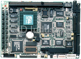
AAEON PCM-4890
Description
All-in-One 486 Single Board Computer with SVGA, Ethernet, and 4 Serial Ports
Part Number
PCM-4890
Price
Request Quote
Manufacturer
AAEON
Lead Time
Request Quote
Category
Single Board Computers
Specifications
System Chipset
VIA VT82C496G
Form Factor
PC/104
Video Chipset
C&T 65545
Datasheet

Extracted Text
PCM-4890
All-in-One 486 Single Board
Computer with SVGA, Ether-
net, and 4 Serial Ports
Copyright Notice
This document is copyrighted, 1997. All rights are reserved. The
original manufacturer reserves the right to make improvements to
the products described in this manual at any time without notice.
No part of this manual may be reproduced, copied, translated or
transmitted in any form or by any means without the prior written
permission of the original manufacturer. Information provided in
this manual is intended to be accurate and reliable. However, the
original manufacturer assumes no responsibility for its use, nor for
any infringements upon the rights of third parties which may result
from its use.
Acknowledgements
VIA is a trademark of VIA Technology, Inc.
AMD is a trademark of Advanced Micro Devices, Inc.
Award is a trademark of Award Software International, Inc.
Cyrix is a trademark of Cyrix Corporation.
IBM, PC/AT, PS/2 and VGA are trademarks of International
Business Machines Corporation.
Intel and Pentium are trademarks of Intel Corporation.
®
Microsoft Windows is a registered trademark of Microsoft Corp.
SMC is a trademark of Standard Microsystems Corporation.
RTL is a trademark of Realtek Semi-Conductor Co., Ltd.
C&T is a trademark of Chips and Technologies, Inc.
UMC is a trademark of United Microelectronics Corporation.
All other product names or trademarks are properties of their
respective owners.
Part No. 2006489007 6th Edition
Printed in Taiwan Dec. 1997
Packing list
Before you begin installing your card, please make sure that the
following materials have been shipped:
• 1 PCM-4890 All-in-One Single Board Computer
• 1 utility disk with system BIOS, VGA BIOS, and Ethernet utility
programs
• 1 utility disk with SVGA utility programs and drivers for Win-
dows 3.1 and Windows 95
• 1 utility disk with Ethernet drivers
If any of these items are missing or damaged, contact your distribu-
tor or sales representative immediately.
FCC STATEMENT
THIS DEVICE COMPLIES WITH PART 15 FCC RULES. OPERA-
TION IS SUBJECT TO THE FOLLOWING TWO CONDITIONS:
(1) THIS DEVICE MAY NOT CAUSE HARMFUL INTERFERENCE.
(2) THIS DEVICE MUST ACCEPT ANY INTERFERENCE RE-
CEIVED INCLUDING INTERFERENCE THAT MAY CAUSE
UNDESIRED OPERATION.
THIS EQUIPMENT HAS BEEN TESTED AND FOUND TO
COMPLY WITH THE LIMITS FOR A CLASS "A" DIGITAL
DEVICE, PURSUANT TO PART 15 OF THE FCC RULES.
THESE LIMITS ARE DESIGNED TO PROVIDE REASONABLE
PROTECTION AGAINTST HARMFUL INTERFERENCE WHEN
THE EQUIPMENT IS OPERATED IN A COMMERCIAL ENVI-
RONMENT. THIS EQUIPMENT GENERATES, USES, AND CAN
RADIATE RADIO FREQENCY ENERGY AND , IF NOT IN-
STATLLED AND USED IN ACCORDANCE WITH THE INSTRUC-
TION MANUAL, MAY CAUSE HARMFUL INTERFERENCE TO
RADIO COMMUNICATIONS. OPERATION OF THIS EQUIP-
MENT IN A RESIDENTIAL AREA IS LIKELY TO CAUSE
HARMFUL INTERFERENCE IN WHICH CASE THE USER WILL
BE REQUIRED TO CORRECT THE INTERFERENCE AT HIS
OWN EXPENSE.
Contents
Chapter 1 General Information ................................ 1
Introduction ........................................................................... 2
Features ................................................................................ 3
Specifications ........................................................................ 3
Standard SBC functions ....................................................... 3
Local-bus flat panel/VGA interface ..................................... 4
Ethernet controller function .................................................. 5
Solid state disk function ........................................................ 5
PC/104 bus expansion .......................................................... 5
Mechanical and environmental ............................................. 5
Board layout and dimensions ................................................ 6
Chapter 2 Installation ................................................ 7
Jumpers and connectors...................................................... 8
Locating jumpers .................................................................. 9
Locating connectors ........................................................... 10
Setting jumpers ................................................................... 11
Safety precautions ............................................................... 12
Installing the CPU............................................................... 12
Removing a CPU ................................................................12
Installing a CPU ..................................................................13
CPU type select (J3-J5, J7, J9-J11).....................................14
CPU power supply select (J1, J2) .......................................16
CPU clock select (J16, J17, J18) .........................................16
CMOS setup (J8) ................................................................16
Buzzer enabled/disabled (J21) ............................................. 16
Installing DRAM (SIMMs) ............................................... 17
Installing SIMMs ................................................................. 17
IDE hard drive connector (CN9) ...................................... 18
Connecting the hard drive .................................................... 18
Floppy drive connector (CN15) ........................................ 19
Connecting the floppy drive ................................................. 19
Parallel port connector (CN12)......................................... 20
Parallel port IRQ .................................................................20
Keyboard and PS/2 connector (CN8) ............................... 20
Front panel connector (CN5) ............................................ 21
Power connectors (CN7, CN10, CN3)............................. 21
Peripheral power connector, -5V, -12V (CN7) ...................21
Main power connector, +5V, +12V (CN10) ........................21
Fan power supply connector (CN3) ....................................21
Serial ports (CN14)............................................................. 22
COM1, COM 3 and COM 4 RS-232 ports (CN14) ............22
COM2 RS-232/422/485 selection (CN14) ........................... 22
VGA interface connections................................................ 23
CRT display connector (CN1) .............................................23
Flat panel display connector (CN2) ..................................... 23
Ethernet configuration ....................................................... 25
10BASE-2/10BASE-5 AUI connector (CN11) ..................25
10BASE-T connector (CN13).............................................26
Network boot .......................................................................26
Watchdog timer configuration ........................................... 27
Watchdog timer enable/disable ............................................ 27
Watchdog timer action (J19, J20) ........................................27
Chapter 3 Software Configuration......................... 29
Introduction ......................................................................... 3 0
Utility disk ............................................................................ 30
VGA display software configuration ................................. 32
Connections for four standard LCDs ............................... 34
Connections to Sharp LM64183P
(640 x 480 DSTN MONO LCD) ........................................34
Connections to Sharp 64C35P
(640 x 480 AD4 EL)............................................................35
Connections to NEC NL8060AC26
(800 x 600 TFT Color LCD) ...............................................36
Connections to Sharp LM64C142
(640 x 480 DSTN Color LCD) ............................................37
Ethernet software configuration ....................................... 38
Chapter 4 Award BIOS Setup ................................... 39
System test and initialization ............................................. 40
System configuration verification ........................................ 40
AWARD BIOS setup........................................................... 41
Entering setup ...................................................................... 41
Standard CMOS setup.........................................................42
BIOS features setup ............................................................43
CHIPSET features setup ....................................................44
Power management setup ...................................................45
Load BIOS Defaults / Load SETUP Defaults ....................46
Change password ................................................................47
Auto detect hard disk ..........................................................48
Save & exit setup ................................................................48
Exit without saving ............................................................... 48
Chapter 5 SVGA Setup .............................................. 49
Simultaneous display mode................................................ 50
Sleep mode........................................................................... 50
Software support.................................................................. 51
Driver installation ............................................................... 52
Windows setup ..................................................................... 53
AutoCAD R12.....................................................................56
Lotus 1-2-3 and Lotus Symphony ........................................ 58
VESA .................................................................................. 60
Word .................................................................................... 61
WordPerfect ........................................................................ 62
Appendix A Programming the Watchdog Timer ... 65
Appendix B Installing PC/104 Modules .................... 67
Installing PC/104 modules................................................. 68
Appendix C Pin Assignments ................................... 71
CRT display connector (CN1) .............................................72
Flat panel display connector (CN2) ..................................... 72
PC/104 connectors (CN4, CN6) .........................................73
Front panel connector (CN5) ..............................................74
Peripheral power connector (CN7) .....................................74
10BASE-2/10BASE-5 AUI connector (CN11) ..................74
COM2 RS-232/422/485 serial port (CN14) ......................... 75
Keyboard and mouse connector (CN8) ..............................75
Ethernet 10BASE-T connector (CN13) ..............................76
Main power connector (CN10) ...........................................76
IDE hard drive connector (CN9) ........................................76
Fan power connector (CN3) ...............................................77
Floppy drive connector (CN15) ........................................... 78
Parallel port connector (CN12) ...........................................79
Appendix D Optional Extras .................................... 81
PCM-10489-1 Cable kit for PCM-4890/5890 ..................... 82
PCM-20486-1 Boot ROM binary files for .........................82
PCM-4890 ...........................................................................82
1
General
Information
This chapter gives background informa-
tion on the PCM-4890.
Sections include:
• Card specifications
• Card layout and dimensions
Chapter 1 General Information 1
CHAPTER
Introduction
The PCM-4890 is an enhanced, all-in-one single board 486 comput-
er with an on-board Ethernet interface, local-bus SVGA controller.
The PCM-4890 offers all the functions of an AT-compatible
industrial computer on a single board, but it fits in the space of a
5¼" floppy drive (only 5.75" x 8"). For maximum performance, the
PCM-4890 also supports 2nd level cache sizes from 128 KB to 512
KB (32 KB x 8, 64 KB x 8, or 128 KB x 8).
On-board features include four serial ports (RS-232 and RS-232/
422/485), one parallel port, an enhanced IDE hard-drive controller
(for up to two drives), a floppy-drive controller and a keyboard/PS/
2 mouse interface. The board's watchdog timer can automatically
reset the system or generate an interrupt if it stops due to a
program bug or EMI problem.
The PCM-4890 also complies with the "Green Function" standard
and supports three types of power saving features: Doze mode,
Standby mode, and Suspend mode.
All display and Ethernet configuration is done through software. A
single Flash chip holds the system BIOS, VGA BIOS and the
network boot ROM function. This minimizes the number of chips
and eases configuration. You can change the display BIOS or
install a boot ROM simply by programming the Flash chip.
If you need any additional functions, you can add up to six
industry-standard PC/104 expansion modules, or use ISA
peripheral cards via the on-board ISA expansion slot.
2 PCM-4890 User's Manual
Features
• Accepts DX2/DX4 and 5x86 CPUs
• Award Flash BIOS, Flat-panel configured by programming Flash chip
• 2nd level cache: supports up to 512 KB cache memory
• 32-bit VL-bus SVGA controller, display both CRT and LCD simulta-
neously
• 16-bit Ethernet interface, Novell NE2000 compatible
• One ISA expansion slot
• Built-in VL bus-master IDE controller supports two IDE devices (large
hard disk, CD ROM, tape backup, etc.)
• Supports both normal and EDO type DRAM from 1 to 64 MB
• One enhanced multi-mode SPP/EPP/ECP parallel port. Four serial ports;
three RS-232 and one RS232/422/485 selectable
• Watchdog timer, time interval 1.6 seconds
• Green function: supports doze, standby and suspend modes
• ISA-bus expansion with PC/104 modules
• Dimensions: 5.75" x 8" (146 mm x 203 mm)
• Single +5 V power supply
• Weight: 0.3 Kg.
Chapter 1 General Information 3
Specifications
Standard SBC functions
• CPU: 80486SX/DX/DX2/DX4/5x86-25/33/40/66/80/100/120/133
• BIOS: AWARD 128 KB Flash memory
• Chipset: VIA VT82C496G
• 2nd level cache: On-board 128 KB, up to 512 KB (SOJ package)
• RAM memory: 1 MB to 64 MB. Two 72-pin SIMM sockets (accepts 1
MB, 2 MB, 4 MB, 8 MB, 16 MB and 32 MB)
• Enhanced IDE hard disk drive interface: Supports up to two IDE (VL-
bus) hard disks. BIOS auto-detect
• Floppy disk drive interface: Supports up to two floppy disk drives, 3½"
(720 KB, 1.44 and 2.88 MB) and/or 5¼" (360 KB and 1.2 MB)
• Multi-mode parallel port: Configured to LPT1, LPT2, LPT3 or disabled.
Supports SPP/ECP/EPP
• Serial ports: Three serial RS-232 port, one serial RS-232/422/485 port.
Ports can be configured as COM1, COM2, COM3, COM4 or disabled
individually. Four 16550 serial UARTs
• Battery: 3.6 V @ 600 mAh lithium battery for up to 10 years of data
retention
• Watchdog timer: Can generate a system reset or IRQ15. Software
enabled/disabled. Time interval is 1.6 seconds
• DMA channels: 7
• Interrupt levels:15
• Keyboard/mouse connector: 8-pin connector supports standard PC/AT
keyboard and a PS/2 mouse
• Power management: I/O peripheral devices support power saving and
doze/standby/suspend modes. AMP 1.1 compliant
4 PCM-4890 User's Manual
Local-bus flat panel/VGA interface
• Chipset: C&T 65545
• Display memory: 512 KB DRAM (standard), 1 MB DRAM (optional)
• Display type: Supports CRT and flat panel (EL, LCD and gas plasma flat
panel) display. Can display CRT and flat panel simultaneously
• CRT display mode: Supports resolutions up to 1024 x 768. Non-inter-
laced CRT monitors resolutions up to 1024 x 768 @ 256 colors. True-
color and Hi-color display capability with flat panels and CRT monitors
at 640 x 480 resolution.
• Panel display modes: Supports resolutions up to 800 x 600 @ 256 colors
(1 MB VRAM)
Ethernet controller function
• Chipset: Realtek RTL8019
• Type: 16-bit Ethernet, Novell NE 2000 compatible
• Connector: 10BASE-T and AUI connector on-board
PC/104 bus expansion
• PC/104: 104-pin connector for a 16-bit bus
• Driving capacity: Six PC/104 modules
• ISA Expansion slot: One ISA slot
Mechanical and environmental
• Power supply voltage: +5 V (4.75 V to 5.25 V)
• Max. power requirements: +5 V @ 4 A (typical)
° °
• Operating temperature: 32 to 140 F (0 to 60 C)
• Board size: 8" (L) x 5.75" (W) (203 mm x 146 mm)
• Weight: 0.3 kg
Chapter 1 General Information 5
�
�
�
�
�
�
Board layout and dimensions
� 5.08 �
� 3.56
�
40.64
�
97.16
�
100.97
�
119.38
�
174.63
�
177.17
�
193.04
�
198.12
�
203.20
Dimensions in mm
PCM-4890 dimensions
6 PCM-4890 User's Manual
�
5.08
�
9.53
95.25
�
135.89
�
140.97
�
146.05
�
�
�
�
�
�
�
�
�
�
� �
�
2
Installation
This chapter tells how to set up the PCM-4890
hardware, including instructions on setting
jumpers and connecting peripherals, switches
and indicators. Be sure to read all the safety
precautions before you begin the installation
procedure.
Chapter 2 Installation 7
CHAPTER
Jumpers and connectors
Connectors on the board link it to external devices such as hard
disk drives, a keyboard, or floppy drives. In addition, the board has
a number of jumpers that allow you to configure your system to
suit your application.
The table below lists the function of each of the board jumpers and
connectors:
Jumpers
Label Function
J1 CPU voltage type selection
J2 3V CPU voltage setting
J3 CPU type setting
J4 CPU type setting
J5 CPU type setting
J6 ECP control
J7 Cyrix CPU or other CPU selection
J8 RTC clear
J9 CPU type jumper settings
J10 CPU type jumper settings
J11 CPU type jumper settings
J12 WT/WB control
J13 CLKMUL control
J14 Clock mode selection
J15 Watchdog timer reset Enable/Disable
J16 Clock Selection
J17 Clock Selection
J18 Clock Selection
J19 Watchdog timer interrupt setting
J20 Watchdog timer Enable/Disable
J21 Buzzer control
J22 ECP control
J23 Printer port interrupt channel selection
J24 COM3 IRQ channel control
J25 COM4 IRQ channel control
J26 Ethernet LED (CRSL)
8 PCM-4890 User's Manual
Jumpers, cont.
Label Function
J27 COM2 RS-232/422/485 selection
J28 Ethernet LED (BNCL)
J29 RS-232/485 setting
J30 RS-232/485 setting
J31 RS-232/485 setting
J32 RS-232/485 setting
J33 COM 4 Voltage Selection
J34 COM 3 Voltage Selection
Connectors
Label Function
CN1 VGA connector
CN2 Flat panel display connector
CN3 Fan power
CN4 PC/104 connector (AT)
CN5 Front panel connector
CN6 PC/104 (XT)
CN7 Peripheral power control
CN8 Keyboard and mouse connector
CN9 IDE connector
CN10 Main power connector
CN11 AUI connector
CN12 Printer connector
CN13 10BaseT connector
CN14 RS-232 connector
CN15 Floppy drive connector
Chapter 2 Installation 9
Locating jumpers
CN11 10Base-2/5 (AUI) Connector
CN9 Enhanced IDE Interface
CN13 Ethernet 10Base-T Connector
CN15 FDD Interface
CN12 Multi-mode Parallel Port
(EPP/ECP/SPP)
CN10 Main Power
CN14 COM Port RS-232 x 3;
RS-232/422/485 x 1
CN8 Keyboard/
Mouse Connector
CN7 Peripheral
Power
CN6 PC/104(XT)
VIA
VT82C496G
CN5 Front Panel
CN3 Fan Power
CN4
PC/104 Connector
CN2 Flat
Panel Display
BAT
INTEL DX4-100(3V)AND Connector
CYRIX 58X6-100
CHIPS
F65545 B2
CN1
CRT Display
Connector
ISA Slot DRAM
10 PCM-4890 User's Manual
J26
J28
J2
J6 J15 J19
20F001N
J9
J1 J3
J12
J4
J13
J5
J14
J7 J10 J11
RTL8019
U1
J27
UMC
UM8663BF
J29J31
J16
J17
J18
J30 J32
J8
SMC
VIA
FDC37C665
VT82C416
J20
J22
J21 J23
J24 J25
Setting jumpers
You configure your card to match the needs of your application by
setting jumpers. A jumper is the simplest kind of electric switch. It
consists of two metal pins and a small metal clip (often protected
by a plastic cover) that slides over the pins to connect them. To
“close” a jumper you connect the pins with the clip. To “open” a
jumper you remove the clip. Sometimes a jumper will have three
pins, labeled 1, 2, and 3. In this case you would connect either pins
1 and 2 or 2 and 3.
3
2
1
Open Closed Closed 2-3
The jumper settings are schematically depicted in this manual as
follows:
1 2 3
Open Closed Closed 2-3
A pair of needle-nose pliers may be helpful when working with
jumpers.
If you have any doubts about the best hardware configuration for
your application, contact your local distributor or sales representa-
tive before you make any changes.
Generally, you simply need a jumper to make most connections.
Chapter 2 Installation 11
Safety precautions
Warning! Always completely disconnect the power cord
from your chassis whenever you are working on it.
Do not make connections while the power is on
because sensitive electronic components can be
damaged by the sudden rush of power. Only
experienced electronics personnel should open
the PC chassis.
Caution! Always ground yourself to remove any static
charge before touching the CPU card. Modern
electronic devices are very sensitive to static
electric charges. Use a grounding wrist strap at all
times. Place all electronic components on a
static-dissipative surface or in a static-shielded
bag when they are not in the chassis.
Installing the CPU
The PCM-4890 all-in-one CPU module supports most 486 CPUs.
The system's performance depends on the CPU you choose. You
can install or upgrade the CPU in the board's PGA socket by
following the procedures outlined below. If your system has an
existing CPU, you need to remove it before installing the new CPU.
Removing a CPU
1. Disconnect power from the chassis, and unplug all connections
to the CPU card. Then, remove the CPU card from the chassis
by following the instructions in the user's manual for your
chassis.
2. Lift the CPU out of the PGA socket. The old chip may be
difficult to remove. You may find spray chip lubricant, designed
for pin-grid-array (PGA) devices, and a chip puller helpful.
These are available at electronics hobbyists' supply stores.
12 PCM-4890 User's Manual
Installing a CPU
To install the CPU, follow the instructions that came with it. If no
documentation was provided, the general procedures for installing
a CPU are outlined below:
1. Lubricate the pins on the CPU with lubricant for PGA devices.
This makes the CPU slide in much easier and greatly reduces
the chance of damaging the pins and other components.
2. Carefully align the CPU so that it is parallel to the socket. Make
sure that the notch on the corner of the CPU matches the notch
on the inside of the socket.
3. Gently push the CPU into the socket. There will probably be a
small gap between the CPU and the socket even when it is fully
seated. DO NOT USE EXCESSIVE FORCE!
When you install a new CPU, you may have to adjust other
settings on the board, such as CPU type, CPU clock, and PCI
speed, to accommodate it. Make sure that the settings are correct
for your CPU. Improper settings may damage the CPU.
Chapter 2 Installation 13
CPU type select (J3, J4, J5, J7, J9, J10, J11)
The following charts show jumper settings for their respective CPUs.
AMD DX2-66 and DX4-100
AMD DX2-66 (clock 33MHz) AMD DX4-100 (clock 33MHz)
J3 J9 J12 J3 J9 J12
J4 J10 J13 J4 J10 J13
J5 J11 J14 J5 J11 J14
J7 J7
AMD 5x86-133 and DX4-120
AMD 5x86-133 (clock 33MHz) AMD DX4-120 (clock 40MHz)
J3 J9 J12 J3 J9 J12
J4 J10 J13 J4 J10 J13
J5 J7 J11 J14 J5 J7 J11 J14
Cyrix DX2-66 and DX2-80
Cyrix DX2-66 (clock 33MHz) Cyrix DX2-80 (clock 40MHz)
J3 J9 J12 J3 J9 J12
J4 J10 J13 J4 J10 J13
J5 J11 J14 J5 J11 J14
J7 J7
Cyrix 5x86-120GP and Intel DX2-66
Cyrix 5x86-120GP (clock 40MHz) Intel DX2-66 (clock P33Mhz)
J3 J9 J12 J3 J9 J12
J4 J10 J13 J4 J10 J13
J5 J11 J14 J5 J7 J11 J14
J7
Intel DX4-100 and Cyrix DX4-100
Intel DX4-100 (clock 33MHz) Cyrix DX4-100 (clock 33Mhz)
J3 J3
J9 J12 J9 J12
J4 J4
J10 J13 J10 J13
J5 J5
J7 J11 J14 J7 J11 J14
14 PCM-4890 User's Manual
CPU power supply select (J1, J2)
J1 and J2 must be set to match the CPU type. The chart below
shows the proper jumper settings for their respective V .
CC
CPU power supply select
3 V 5 V
1 3 5 1 3 5
J1
2 4 6
2 4 6
*3.3 V 3.45 V 3.6 V
1 3 5 1 3 5 1 3 5
J2
2 4 6
2 4 6 2 4 6
CPU clock select (J16, J17, J18)
J16, J17, and J18 are used to synchronize the CPU clock with the
CPU type. Set the CPU clock according to the base CPU speed.
CPU clock select
25 MHz *33 MHz 40 MHz
J16
J17
1 2 3
J18 1 2 3 1 2 3
CMOS setup (J8)
CMOS setup
*3.6V Battery On Clear CMOS
J8
1 2 3 1 2 3
Buzzer enabled/disabled (J21)
Buzzer enabled/disabled
Enable Disable
J21
1 2 1 2
* default setting
Chapter 2 Installation 15
CPU frequency ratio (J13, J14)
CLKMUL Control
2x system frequency 1x system frequency
J13
1 2 1 2
J14
1 2 1 2
Cache Mode WB/WT (J12)
WT WB
J12 1 2
1 2
Watchdog timer reset Enable/Disable
(J15)
Enable Disable
J15
1 2 1 2
16 PCM-4890 User's Manual
Installing DRAM (SIMMs)
You can install anywhere from 1 MB to 32 MB of on-board DRAM
memory using 1, 2, 4, 8 or 16 MB 72-pin SIMMs (Single In-Line
Memory Modules). Access time should be 70 nsec. or less.
Memory installs in two banks composed of one SIMM socket each.
The banks are designated as Bank0 and Bank1. See the figure on
page 10 for help identifying the banks. You must fill Bank0 first. If
you fill both banks, the memory capacity of both SIMMs should be
the same.
Installing SIMMs
NOTE: The modules can only fit into a socket one way.
Their chips must face the CPU, and their gold
pins must point down into the SIMM socket.
The procedure for installing SIMMs appears below. Please follow
these steps carefully.
1. Ensure that all power supplies to the system are switched Off.
2. Locate the board's memory banks, shown in the figure on
page 9.
3. Install the SIMM cards. Install each SIMM so that its chips
face away from the CPU and its gold pins point down into the
SIMM socket.
4. Slip each SIMM into a socket at a 45 degree angle and carefully
fit the bottom of the card against the connectors.
5. Gently push the SIMM into a perpendicular position until the
clips on the ends of the SIMM sockets snap into place.
6. Check to ensure that each SIMM is correctly seated and all
connector contacts touch. The SIMM should not move around
in its socket.
Chapter 2 Installation 17
IDE hard drive connector (CN9)
The built-in Enhanced IDE (Integrated Device Electronics) control-
ler supports up to two IDE devices, including CD-ROM drives, tape
backup drives, a large hard disk drive and other IDE devices. It also
supports faster data transfer rates and allows the IDE hard disk
drive to exceed 528 MB.
Connecting the hard drive
Connecting drives is done in a daisy-chain fashion and requires
one of two cables, depending on the drive size. 1.8" and 2.5" drives
need a 1 x 44-pin to 2 x 44-pin flat-cable connector. 3.5" drives use a
1 x 44-pin to 2 x 40-pin connector.
Wire number 1 on the cable is red or blue, and the other wires are
gray.
1. Connect one end of the cable to CN9. Make sure that the red (or
blue) wire corresponds to pin 1 on the connector, which is
labeled on the board (on the right side).
2. Plug the other end of the cable to the Enhanced IDE hard drive,
with pin 1 on the cable corresponding to pin 1 on the hard
drive. (See your hard drive's documentation for the location of
the connector.)
Connect a second drive as described above.
Unlike floppy drives, IDE hard drives can connect to either end of
the cable. If you install two drives, you will need to set one as the
master and one as the slave by using jumpers on the drives. If you
install just one drive, set it as the master.
18 PCM-4890 User's Manual
Floppy drive connector (CN15)
You can attach up to two floppy disks to the PCM-4890's on-board
controller. You can use any combination of 5¼" (360 KB and 1.2
MB) and/or 3½" (720 KB, 1.44 MB, and 2.88 MB) drives.
A 34-pin daisy-chain drive connector cable is required for a dual-
drive system. On one end of the cable is a 34-pin flat-cable connec-
tor. On the other end are two sets of floppy disk drive connectors.
Each set consists of a 34-pin flat-cable connector (usually used for
3½" drives) and a printed-circuit board connector (usually used for
5¼" drives).
Connecting the floppy drive
1. Plug the 34-pin flat-cable connector into CN15. Make sure that
the red wire corresponds to pin one on the connector.
2. Attach the appropriate connector on the other end of the cable
to the floppy drive(s). You can use only one connector in the
set. The set on the end (after the twist in the cable) connects to
the A: drive. The set in the middle connects to the B: drive.
3. If you are connecting a 5¼" floppy drive, line up the slot in the
printed circuit board with the blocked-off part of the cable
connector.
If you are connecting a 3½" floppy drive, you may have trouble
determining which pin is pin number one. Look for a number
printed on the circuit board indicating pin number one. Also,
the connector on the floppy drive connector may have a slot.
When the slot is up, pin number one should be on the right.
Check the documentation that came with the drive for more
information.
If you desire, connect the B: drive to the connectors in the
middle of the cable as described above.
If you need to make your own cable, you can find the pin assign-
ments for the card’s connector in Appendix C.
Chapter 2 Installation 19
Parallel port connector (CN12)
Normally the parallel port is used to connect the card to a printer.
The PCM-4890 includes an on-board parallel port, accessed
through CN12, a 26-pin flat-cable connector. You will need an
adapter cable if you use a DB-25 connector. The cable has a 26-pin
connector on one end and a DB-25 connector on the other.
Parallel port IRQ
The PCM-4890 supports one parallel port. The port is designated
as LPT1 and can be disabled or changed to LPT2 or LPT3 in the
system BIOS setup.
Parallel port IRQ selection
IRQ5 *IRQ7
J23
1 2 2 3
You can select ECP/EPP DMA channel by setting J15 and J16.
ECP/EPP DMA channel
*DMA1 DMA3
J6
J22
1 2 2 3
* default setting
Keyboard and PS/2 connector (CN8)
The PCM-4890 board provides a keyboard connector which
supports both a keyboard and a PS/2 style mouse. In most cases,
especially in embedded applications, a keyboard is not used. The
standard PC/AT BIOS will report an error or fail during power-on
self test (POST) after a reset if the keyboard is not present. The
PCM-4890's BIOS standard setup menu allows you to select "All,
But Keyboard" under the "Halt On" selection. This allows no-
keyboard operation in embedded system applications without the
system halting under POST (power-on-self-test).
20 PCM-4890 User's Manual
Front panel connector (CN5)
Next you may want to install external switches to monitor and
control the PCM-4890. These features are completely optional —
install them only if you need them. The front panel connector (CN5)
is an 8-pin male, dual in-line header and provides connections for a
speaker, hard disk access indicator and an input switch for reset-
ting the card.
Speaker
The PCM-4890 can drive an 8 W speaker at 0.5 watts. Ensure that
alternatives to this specification do not overload the card.
LED interface
The front panel LED indicator for hard disk access is an active low
signal (24 mA sink rate).
Reset switch
If you install a reset switch, it should be a open single pole switch.
Momentarily pressing the switch will activate a reset. The switch
should be rated for 10 mA, 5 V.
If you need to make your own cable, you can find the pin assign-
ments for the card’s connector in Appendix C.
Power connectors (CN7, CN10, CN3)
Peripheral power connector, -5V, -12V
(CN7)
Supplies secondary power to devices that require -5 V and -12 V.
Main power connector, +5V, +12V
(CN10)
Supplies main power to the PCM-4890 (+5 V) and devices that
require +12 V.
Fan power supply connector (CN3)
Provides power supply to optional CPU cooling fan. Only present
when +5 V and +12 V power is supplied to the board.
Chapter 2 Installation 21
Serial ports (CN14)
The PCM-4890 offers four serial ports: three RS-232 and one RS-
232/422/485. These ports let you connect to serial devices (a
mouse, printers, etc.) or a communication network.
COM1, COM3, COM4 RS-232 ports (CN14)
The serial port connectors are mounted on the right hand side of
the card. The 40-pin, dual-in-line, male header to the right of the
card is the RS-232/422/485 port.
COM2 selection (J27)
*RS-232 RS-422 RS-485
1 2
1 2 1 2
3 4 3 4
3 4
J27
5 6 5 6 5 6
* default setting
COM3 IRQ channel control (J24)
IRQ 5 IRQ 10
J24
1 2 3 1 2 3
COM4 IRQ channel control (J25)
IRQ 5 IRQ 10
J25
1 2 3 1 2 3
RS-232/RS-422/RS-485 setting (29, J30, J31, J32)
RS-232 RS-422/RS-485
1 2 3 1 2 3
COM 3,4 Voltage selection
RING +5V +12V
1 3 5 1 3 5 1 3 5
22 PCM-4890 User's Manual
The IRQ and address range for both ports are fixed. However if you
wish to disable the port or change these parameters later you can
do this in the system BIOS setup. The table below shows the
settings for the PCM-4890's ports.
PCM-4890 Serial port default settings
Port Address Range Interrupt Default
COM1 2E8~3F8 IRQ4 3F8
COM2 2E8~3F8 IRQ3 2F8
COM3 IRQ5/10 2EF
COM4 IRQ5/10 2E8
VGA interface connections
The PCM-4890's SVGA interface can drive conventional CRT
displays and is capable of driving a wide range of flat panel
displays, including electroluminescent (EL), gas plasma, passive
LCD and active LCD displays. The card has two connectors to
support these displays, one for standard CRT VGA monitors and
one for flat panel displays.
CRT display connector (CN1)
CN1 is a 16-pin, dual-in-line header used for conventional CRT
displays. A simple one-to-one adapter can be used to match CN1 to
a standard 15-pin D-SUB connector commonly used for VGA.
Pin assignments for CRT display connector CN1 are detailed in
Appendix C.
Flat panel display connector (CN2)
CN2 consists of a 44-pin, dual-in-line header. Power supplies (+12 V,
-12 V) present on CN2 depend the supply connected to the board.
Ensure that both CN7 and CN10 are connected for
±12 V power supply.
Chapter 2 Installation 23
The PCM-4890 provides a bias control signal on CN2 which can be
used to control the LCD bias voltage. It is recommended that the
LCD bias voltage not be applied to the panel until the logic supply
voltage (+5 V) and panel video signals are stable. Under normal
operation the control signal (ENAVEE) is active high. When the
PCM-4890's power is applied, the control signal is low until just
after the relevant flat panel signals are present.
Configuration of the VGA interface is done completely via the
software utility. You don't have to set any jumpers. Refer to Chapter
3 for software setup details.
Refer to Chapter 3 for details on connecting the four standard
LCD's: Sharp LM64183P, Toshiba LTM09C016, Sharp 64C142, and
Planor EL Display.
24 PCM-4890 User's Manual
Ethernet configuration
The PCM-4890 is equipped with a high performance 16-bit Ethernet
interface which is fully compliant with IEEE 802.3 10Mbps CSMA/
CD standards. It is supported by all major network operating
systems and is 100% Novell NE-2000 compatible.
Configuration of the Ethernet is very easy and can be done via the
RSET8019.EXE program included on the utility disk. This program
enables you to: view the current Ethernet configuration, to recon-
figure the Ethernet interface (IRQ, I/O address, etc.), and to execute
useful diagnostic functions. (See Chapter 3 for detailed informa-
tion)
The RSET8019.EXE program provides two ways to configure the
Ethernet interface. Configuration can be done automatically when
you choose PNP (plug and play) option; or, when you choose the
Jumperless option, the following IRQ and I/O address settings are
available.
PCM-4890 Ethernet settings
IRQ option I/O address
range
Jumperless 2, 3, 4, 5, 10, 200 - 300 EFH
Configuration 11, 12, 15
Default Settings: IRQ = 3 ; I/O Address = 300H
Note: 1. You can select an IRQ from the options shown
above, but make sure your selection does not
conflict with other I/O devices.
2. When Boot ROM is installed, the
RSET8019.EXE program does not support PNP
mode configuration.
10BASE-2/10BASE-5 AUI connector (CN11)
10BASE-2 and 10BASE-5 coax connections are made via an
attachment unit interface or AUI (CN11). This consists of a 16-pin,
dual-in-line male header.
Chapter 2 Installation 25
10BASE-T connector (CN13)
10BASE-T connects to the PCM-4890 via an adapter cable to a 10-
pin polarized header (CN13). For 10BASE-T RJ-45 operation, an
adapter cable converting CN13 into a standard RJ-45 jack is
required.
Network boot
The Network Boot feature can be utilized by incorporating the Boot
ROM image files for the appropriate network operating system. The
Boot ROM BIOS files are available from your supplier. They can be
programmed into the BIOS, similar to the VGA BIOS file, using the
AWDFLASH.EXE program detailed in Chapter 3.
26 PCM-4890 User's Manual
Watchdog timer configuration
An on-board watchdog timer reduces the chance of disruptions
which EMP (electro-magnetic pulse) interference can cause. This is
an invaluable protective device for standalone or unmanned
applications. Setup involves two jumpers and running the control
software (refer to Appendix A).
Watchdog timer enable/disable
You can enable or disable the watchdog timer by reading the
I/O ports with your program. Read address 443 hex to enable and
refresh the watchdog or address 043 to disable the watchdog. For
information on programming the watchdog timer see Appendix A.
Watchdog timer action (J19, J20)
When the watchdog timer activates (CPU processing has come to a
halt), it can reset the system or generate an interrupt on IRQ15.
This can be set via two 2-pin jumpers (J19, J20) as shown below:
Watchdog timer system reset/IRQ15
*System reset IRQ15
J19
* default setting
Watchdog timer enable/disable
Enable Disable
J20
Chapter 2 Installation 27
28 PCM-4890 User's Manual
3
Software
Configuration
This chapter details the software configu-
ration information. It shows you how to
configure the card to match your applica-
tion requirements. AWARD System BIOS
is covered in Chapter 4.
Sections include:
• LCD display configuration
• Connections for four standard LCDs
• Ethernet interface configuration
Chapter 3 Software Configuration 29
CHAPTER
Introduction
The PCM-4890 system BIOS and custom drivers are located in a
128 Kbyte, 32-pin (JEDEC spec.) Flash ROM device, designated
U27. A single Flash chip holds the system BIOS, VGA BIOS, and
network Boot ROM image. The display can be configured via
software. This method minimizes the number of chips and eases
configuration. You can change the display BIOS simply by
reprogramming the Flash chip.
Utility disk
The PCM-4890 is supplied with a software utility disk. This disk
contains the necessary file for setting up the VGA display and
Ethernet controller. Directories and files on the disk are as follows:
README.DOC
COOKROM.EXE
NET (Dir) RSET8019.EXE
PG8019.EXE
8019.CFG
DISPLAY (Dir) AWDFLASH.EXE
4890_SYS.BIN
4890_CRT.BIN
4890_TFT.BIN
4890_STN.BIN
4890_ST5.BIN
4890_MON.BIN
4890_EL.BIN
CDROM.EXE
COOKROM.EXE
A program that converts application files into binary files (files
with a .BIN extension). These are then written into the SSD Flash
ROM devices.
RSET8019.EXE
This program enables you to view the current Ethernet configura-
tion, reconfigure the Ethernet interface (medium type, etc.), and
execute useful diagnostic functions.
30 PCM-4890 User’s Manual
PG8019.EXE
The PCM-4890 is initially setup at the factory using this program.
When you receive your card, use RSET8019.EXE to configure for
the working environment. If by chance the EEPROM is corrupted,
the PG8019.EXE program allows you to reconfigure the card.
8019.CFG
When you run PG8019.EXE, it will read the configuration
parameters stored in this file.
AWDFLASH.EXE
This program allows you to write the VGA BIOS files to the BIOS
Flash ROM. The VGA files all come ready formatted for the
PCM-4890 with .BIN extensions. See README.DOC. These files
support various CRT and flat panel displays. They are custom
written and can be made available upon request.
4890_SYS.BIN
This binary file contains the system BIOS.
4890_CRT.BIN
Supports CRT only.
4890_TFT.BIN (default)
Supports 640 x 480 color TFT
(Sharp LQ9D011, Toshiba LTM09C015A/016).
4890_STN.BIN (1 MB VRAM)
Supports 640 x 480 color STN DD 8/16-bit displays
(Sharp LM64C142).
4890_ST5.BIN (512 KB VRAM)
Supports 640 x 480 color STN DD 8/16-bit displays
(Sharp LM64C142).
NOTE: This BIOS does not support simultaneous CRT
and flat panel display with 512 KB VRAM
4890_MON.BIN
Supports 640 x 480 dual scan monochrome displays
(Sharp LM64P8X/837).
Chapter 3 Software Configuration 31
4890_EL.BIN
Supports 640 x 480 EL displays (PLANAR EL640480 - A Series).
CBROM.EXE
This program allows you to combine your own VGA BIOS with
system BIOS (4890_SYS.BIN).
VGA display software configuration
The PCM-4890’s on-board VGA interface supports a wide range
of popular LCD, EL, gas plasma flat panel displays and traditional
analog CRT monitors. The interface can drive CRT displays with
resolutions up to 1024 x 768 in 256 colors. It is also capable of
driving color panel displays with resolutions of 640 x 480 in 64K
colors. The VGA interface is configured completely via the
software utility, so you don’t have to set any jumpers. Configure
the VGA display as follows:
1. Apply power to the PCM-4890 with a color TFT display
attached. This is the default setting for the PCM-4890. Ensure
that the AWDFLASH.EXE and *.BIN files are located in the
working drive.
NOTE: Ensure that you do not run AWDFLASH.EXE
while your system is operating in EMM386 mode.
32 PCM-4890 User’s Manual
2. At the prompt, type AWDFLASH.EXE and press immediately. This will
allow you to enter Setup.
Chapter 4 Award BIOS Setup 41
Standard CMOS setup
When you choose the STANDARD CMOS SETUP option from
the INITIAL SETUP SCREEN menu, the screen shown below is
displayed. This standard Setup Menu allows users to configure
system components such as date, time, hard disk drive, floppy
drive, display, and memory. Once a field is highlighted, on-line
help information is displayed in the left bottom of the Menu
screen.
R O M I S A B I O S ( 2 C 4 L 6 A K L )
S T A N D A R D C M O S S E T U P
A W A R D S O F T W A R E , I N C .
Date (mm:dd:yy) : Wed, Jan 17 1996
Time (hh:mm:ss) : 12 : 19 : 58
TYPE SIZE CYLS. HEADS PRECOMP LANDZONE SECTORS MODE
Drive C : Auto 0 0 0 0 0 0 Auto
Drive D : Auto 0 0 0 0 0 0 Auto
Drive A : 1.44M, 3.5in Base Memory : 640K
Drive B : None Extended Memory : 3072K
Other Memory : 384K
Video : EGA/VGA
Halt On : All Errors
Total Memory : 4096K
ESC : Quit ��� : Select Item PU / PD / + / - : Modify
F1 : Help (Shift)F2 : Change Color
CMOS setup screen
42 PCM-4890 User’s Manual
BIOS features setup
By choosing the BIOS FEATURES SETUP option from the
INITIAL SETUP SCREEN menu, the screen below is displayed.
This sample screen contains the system configurations based on
BIOS DEFAULT settings for the PCM-4890.
R O M I S A B I O S ( 2 C 4 L 6 A K L )
B I O S F E A T U R E S S E T U P
A W A R D S O F T W A R E , I N C .
Virus Warning : Disabled Video BIOS Shadow : Enabled
CPU Internal Cache : Enabled C8000-CBFFF Shadow : Disabled
External Cache : Enabled CC000-CFFFF Shadow : Disabled
Quick Power On Self Test : Disabled D0000-D3FFF Shadow : Disabled
Boot Sequence : A,C D4000-D7FFF Shadow : Disabled
Swap Floppy Drive : Disabled D8000-DBFFF Shadow : Disabled
Boot Up Floppy Seek : Enabled DC000-DFFFF Shadow : Disabled
Boot Up NumLock Status : On
Boot Up System Speed : High
IDE HDD Block Mode : Disabled
Gate A20 Option : Normal
Memory Parity Check : Disabled
Typematic Rate Setting : Disabled
Esc : Quit ���: Select Item
Typematic Rate (Chars/Sec) : 6
F1 : Help PU / PD / + / - : Modify
Typematic Delay (Msec) : 250
F5 : Old Values (Shift)F2 : Color
Security Option : Setup
F6 : Load BIOS Defaults
OS Select For DRAM>64MB : Non-OS2
F7 : Load Setup Defaults
BIOS features setup
Chapter 4 Award BIOS Setup 43
CHIPSET features setup
By choosing the CHIPSET FEATURES SETUP option from the
INITIAL SETUP SCREEN menu, the screen below is displayed.
This sample screen contains the system configurations based on
BIOS DEFAULT settings for the PCM-4890.
R O M I S A B I O S ( 2 C 4 L 6 A K L )
C M O S S E T U P U T I L I T Y
C H I P S E T F E A T U R E S S E T U P
Auto Configuration : Enabled
On-Board Local-Bus IDE : Enabled
Decoupled Refresh : Disabled IDEPrimary Master PIO : Auto
Relocate 256K/384K : Disabled IDE Primary Slave PIO : Auto
Video BIOS Cacheable : Disabled
System BIOS Cacheable : Disabled
On-Board FDC Controller : Enabled
On-Board Serial Port 1 : 3F8H
External Cache Scheme : Write Back On-Board Serial Port 2 : 2F8H
Combine Alter & Tag Bits : Disabled COM3 & COM4 Address : 3E8H,2E8H
CHRDY for ISA Master : Enabled
On-Board Parallel Port : 378H
Memory Hole At 15 MB Addr. : Disabled
Parallel Extended Mode : Normal
Cache Timing Control : Fast
DRAM Timing Control : Normal
Fast DRAM : Disabled
Burst Write : Disabled
Esc : Quit ���: Select Item
CPU Write Back Cache : Disabled
F1 : Help PU/PD/+/- : Modify
Set Turbo Pin Function : Suspend
F5 : Old Values (Shift)F2 : Color
Set Mouse Lock : Disabled
F6 : Load BIOS Defaults
CHIPSET features setup
44 PCM-4890 User’s Manual
Power management setup
By choosing the POWER MANAGEMENT SETUP option from
the INITIAL SETUP SCREEN menu, the screen below is dis-
played. This sample screen contains the system configurations
based on BIOS DEFAULT settings for the PCM-4890.
R O M I S A B I O S ( 2 C 4 L 6 A K L )
C M O S S E T U P U T I L I T Y
P O W E R M A N A G E M E N T S E T U P
Power Management : Disabled IRQ3 Activity : Primary
Doze Mode : 32 sec IRQ4 Activity : Primary
IRQ5 Activity : Primary
Sleep Timer : 2 min IRQ7 Activity : Primary
Sleep Mode : Suspend IRQ8 Activity : Secondary
HDD Power Management : Disabled
IRQ10 Activity : Primary
VGA Activity Wakeup : Disabled
IRQ11 Activity : Primary
IRQ12 Activity : Primary
IO Activity : Disabled
Video Off Method : Blank Screen
Esc : Quit
��� : Select Item
F1 : Help PU/PD/+/- : Modify
F5 : Old Values (Shift)F2 : Color
F6 : Load BIOS Defaults
Power management setup
Chapter 4 Award BIOS Setup 45
Load BIOS Defaults/Load SETUP Defaults
LOAD BIOS DEFAULTS loads the default system values directly
from ROM. The BIOS DEFAULTS provides the most stable
settings, though they do not provide optimal performance. LOAD
SETUP DEFAULTS, on the other hand, provides for maximum
system performance. If the stored record created by the Setup
program becomes corrupted (and therefore unusable), BIOS
defaults will load automatically when you turn the PCM-4890 on.
R O M I S A B I O S ( 2 C 4 L 6 A K L )
C M O S S E T U P U T I L I T Y
A W A R D S O F T W A R E , I N C .
STANDARD CMOS SETUP PASSWORD SETTING
BIOS FEATURES SETUP IDE HDD AUTO DETECTION
CHIPSET FEATURES SETUP SAVE & EXIT SETUP
POWER MANAGEMENT SETUP EXIT WITHOUT SAVING
LOAD BIOS DEFAULTS
LOAD SETUP DEFAULTS
Load BIOS Defaults (Y/N)? Y
ESC: QUIT ���:SELECT ITEM
F10:Save & Exit Setup (Shift)F2:Change Color
Load BIOS defaults except standard CMOS SETUP
Load BIOS defaults screen
46 PCM-4890 User’s Manual
Change password
To change the password, choose the PASSWORD SETTING
option form the Setup main menu and press
Frequently asked questions
How does Industrial Trading differ from its competitors?

Is there a warranty for the PCM-4890?
Which carrier will Industrial Trading use to ship my parts?
Can I buy parts from Industrial Trading if I am outside the USA?
Which payment methods does Industrial Trading accept?
Why buy from GID?

Quality
We are industry veterans who take pride in our work

Protection
Avoid the dangers of risky trading in the gray market

Access
Our network of suppliers is ready and at your disposal

Savings
Maintain legacy systems to prevent costly downtime

Speed
Time is of the essence, and we are respectful of yours
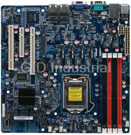
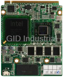
Related Products
486DX5-133 Half-size CPU Card with LCD, Ethernet, & SSD
VIA C3 / Eden Low Power Processors
Compact Board with Intel Pentium 4/ Celeron Processors
Entry Level Intel Xeon Server Board, UDIMM RAM/VGA/GbE x 2 LAN/2 USB
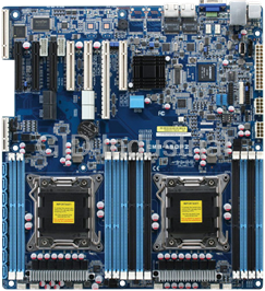
High Performance Server Board with Dual Intel Xeon Processors, RDIMM/UDIMM/LRDIMM RAM, VGA, 2 GbE LA...
Request a Quote

The quote request has been received
Close

Facing challenges or have inquiries? Feel free to contact us!
Call Us +1-469-283-2440
What they say about us
FANTASTIC RESOURCE
One of our top priorities is maintaining our business with precision, and we are constantly looking for affiliates that can help us achieve our goal. With the aid of GID Industrial, our obsolete product management has never been more efficient. They have been a great resource to our company, and have quickly become a go-to supplier on our list!
Bucher Emhart Glass
EXCELLENT SERVICE
With our strict fundamentals and high expectations, we were surprised when we came across GID Industrial and their competitive pricing. When we approached them with our issue, they were incredibly confident in being able to provide us with a seamless solution at the best price for us. GID Industrial quickly understood our needs and provided us with excellent service, as well as fully tested product to ensure what we received would be the right fit for our company.
Fuji
HARD TO FIND A BETTER PROVIDER
Our company provides services to aid in the manufacture of technological products, such as semiconductors and flat panel displays, and often searching for distributors of obsolete product we require can waste time and money. Finding GID Industrial proved to be a great asset to our company, with cost effective solutions and superior knowledge on all of their materials, it’d be hard to find a better provider of obsolete or hard to find products.
Applied Materials
CONSISTENTLY DELIVERS QUALITY SOLUTIONS
Over the years, the equipment used in our company becomes discontinued, but they’re still of great use to us and our customers. Once these products are no longer available through the manufacturer, finding a reliable, quick supplier is a necessity, and luckily for us, GID Industrial has provided the most trustworthy, quality solutions to our obsolete component needs.
Nidec Vamco
TERRIFIC RESOURCE
This company has been a terrific help to us (I work for Trican Well Service) in sourcing the Micron Ram Memory we needed for our Siemens computers. Great service! And great pricing! I know when the product is shipping and when it will arrive, all the way through the ordering process.
Trican Well Service
GO TO SOURCE
When I can't find an obsolete part, I first call GID and they'll come up with my parts every time. Great customer service and follow up as well. Scott emails me from time to time to touch base and see if we're having trouble finding something.....which is often with our 25 yr old equipment.
ConAgra Foods